New Results on ATLAS Pixel Opto-Link
Abstract:
We present new results on the optical link for the pixel detector of the ATLAS experiment. An optical package of novel design has been developed for the opto-link. The design is based on a simple connector-type concept and is made of radiation-hard material. The receiver (DORIC) and transmitter (VDC) chips have been designed. The prototype results using the 0.8 and 0.25 m technologies are presented.
The ATLAS pixel detector [1] consists of three barrel layers and three forward and backward disks. The detector covers the pseudo-rapidity region and provides at least three space point measurements. The low voltage differential signal (LVDS) from the pixel detector is converted by the VCSEL Driver Chip (VDC) into a single-ended signal appropriate to drive a Vertical Cavity Surface Emitting Laser (VCSEL). The optical signal is transmitted to the Readout Device (ROD) via a fibre. For the innermost barrel layer, the signal is transmitted using two fibres. The 40-MHz beam crossing clock from the ROD, bi-phase encoded with the command signal to control the pixel detector, is transmitted to a PIN diode via a fibre. The PIN signal is decoded using a Digital Opto-Receiver Integrated Circuit (DORIC). The VSCEL and PIN diodes couple to the fibres inside optical packages. In this paper, we describe the performance of the opto-pack developed by The Ohio State University (OSU) group and status of the VDC and DORIC prototypes.
1 Results on Opto-Packs
The main technical challenge in the fabrication of the opto-pack is the alignment tolerance of the VCSEL with respect to the fibre:
50 m in (along the fibre)
25 m in (transverse to the fibre)
The requirements can be satisfied either by passive or active alignment. For the former, parts must be fabricated or placed with high precision (m) so that the overall precision is still within the tolerance. The alignment tolerance of the PIN to the fiber is much looser. There were two designs for the opto-pack, OSU and Academia Sinica (Taiwan), using passive and active alignment, respectively.
In the Taiwan design, the fiber is cleaved at 45o to act as a mirror. Light traveling down the fiber is reflected onto the PIN placed directly below the cleaved surface. Conversely, light emitted by a VCSEL is reflected off the cleaved surface into the fiber. Each fiber is actively aligned and glued permanently to the package. The package is of low cost but the permanent attachment of the fibers to the package presents a technical challenge to the assembly of the pixel detector.
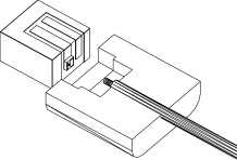
The OSU design uses a connector concept: a cap with a hole for the fibre and a base with deposited wire bonding trace and pad for PIN or VCSEL placement. The design is shown in Fig. 1. The package is of low cost and the cap with the fiber attached can be mounted on the base near the end of the pixel detector assembly. Precise alignment of the VCSEL to the fiber is achieved by fabricating the bases and caps with high precision and by the accurate placement of the VCSEL and fibre relative to the base and cap, respectively.
The base is made of aluminia. To fabricate the base, aluminia sheet is ground to the precise thickness of the base and then cut into strips for deposition of three-dimensional traces [2]. Most of the deposited traces have good connectivity across the corner of the base. Strips with a large number of traces of good connectivity were then precisely diced into individual bases [3].
The cap is made of Ultem (polyetherimide), a mold-injectable plastic with a radiation tolerance [4] of 10 GRad. Due to the high cost and long lead time in developing the injection molding technique for fabricating small parts with high precision, we decided to use “manual mold injection”. Here a small spring-loaded mold of 5 cm 5 cm 10 cm is used in a small oven as opposed to a standard mold of 30 cm 30 cm 30 cm placed inside an automatic mold injection machine of 1 m 1 m 2 m. The critical part in the mold fabrication is the precisely machined mold for the interior of the cap that fits the base and the precisely located hole for the placement of a pin which produces the hole for the fiber. We have proven the principle of this precise micro-mold injection technique and can fabricate several quality caps per hour.
The VCSEL is precisely placed on the base under an optical comparator. To further improve the alignment between the fiber and the VCSEL, the location of the pin on the mold is also measured so that the VCSEL is placed on the base at the location as expected from the fabricated cap. In addition, the dimension of each base is measured individually so that the location of the VCSEL is adjusted slightly to account for the small variation in size.
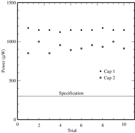
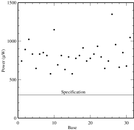
We have fabricated 31 VCSEL opto-packs. Figure 2 shows the measured coupled power. The coupled power of all packages are above the specification of 300 W minimum power for an average current of 10 mA in the VCSEL. The average coupled power is 760 W. The caps can also be used multiple times. Figure 3 shows the coupled power of two typical caps for each of the 10 mountings on a base. Each mounting gives about the same coupled power. The caps are also interchangeable. Figure 4 shows the coupled power of a cap on the 31 bases. The cap gives about the same coupled power on all bases. This proves the feasibility of the connector-type design. The waveforms of the mounted VCSELs also have fast rise time, 1ns. We have fabricated two PIN opto-packs with three PINs in each package. The PIN diodes have good responsivity, 0.5 A/W. The opto-packs therefore meets the pixel detector specification.

There was a review of the OSU and Taiwan opto-packs in June. The Taiwan opto-pack potentially has 10-15% higher coupled power and has been chosen as the baseline in order to take advantage of the additional resources from Taiwan.
2 Results on Optical Chips
The pixel detector design of the VDC and DORIC takes advantage of the development work for similar chips used by the outer detector, the SemiConductor Tracker (SCT). Both SCT chips attain radiation-tolerance by using bipolar integrated circuits (AMS 0.8 m BICMOS) and running with high currents in the transistors. The chip is therefore not applicable for the higher radiation dosage and lower power budget requirements of the pixel detector. We design the radiation-hard CMOS version of the circuits in collaboration [5] with University of Siegen, Germany.
The first pixel version of the chips with 0.8 m feature size was submitted to DMILL in July 1999. VDC functioned well but DORIC could not decode the clock properly. The problem was due to underestimate of the parasitic capacitance.
The second version of the chips was submitted to DMILL in July 2000. Both chips worked but for some of the DORICs the pre-amp output was observed to be saturated with no input signal, indicating that there was an offset between the differential pre-amp inputs due to process variations. We submitted to DMILL in May 2001 a new design with a DC feedback circuit between the output and input of the pre-amp to cancel the offset. We expect the delivery of the chips in November 2001.
In April 2001, we irradiated 14 chips from the second DMILL run with 24 GeV protons at CERN. Some of the chips can operate up to 50 Mrad by increasing the supply voltage from 3.2 to 5.0 V but others died within a few Mrad. Annealing at 100oC for a week failed to improve or revive the chips. This indicates that the chips may not be adequate for the pixel detector as we expect the optical link to receive a dosage of 20 Mrad.
We have converted the DMILL design into a design with smaller feature size, 0.25 m, using a different vendor. This process is expected to be more radiation hard than the DMILL process. The new designs were submitted in February 2001. The VDC works well with fast rise and fall time ( 1 ns) but consumes more current than we would like. We plan to reduce the current consumption by several mA in the next submission expected in the Fall 2001. For the DORIC, the delay control circuit oscillates. We are not able to reproduce the oscillation in the simulation. The oscillation can be cured with an external bypass capacitor and then the chips decode the bi-phase marked clock properly. Some chips require a large input PIN signal due to the large pre-amp offset from process variations. The DC feedback circuit can cancel part of the offset; this has been verified by adjusting the amount of DC feedback. We will increase the amount of feedback in the next submission. We plan to irradiate the chips with 24 GeV protons at CERN in September 2001.
3 Summary
We have developed an opto-pack based on the novel connector-type concept for the pixel detector of the ATLAS experiment. The opto-pack meets the specification but the Taiwan design was chosen as the baseline to take advantage of their resources. We have designed versions of the VDC and DORIC in the 0.8 and 0.25 m technology. The chips are functional but further improvements are planned. The design in the 0.8 m technology appears inadequate in radiation hardness for the ATLAS pixel detector.
Acknowledgments.
This work was supported in part by the U.S. Department of Energy. The author wishes to thank K.E. Arms, K. Arndt, J. Burns, H.P. Kagan, R.D. Kass, S. Smith, T. Weidberg, and R. Wells for their contributions to the development of the opto-packs.References
- [1] ATLAS Pixel Detector Technical Design Report, CERN/LHCC/98-13.
- [2] Hybrid-Tek Inc., 1 Hytek Corporate Ctr, Rte. 526, Clarksburg, NJ 08510, USA.
- [3] American Dicing Inc., 344 East Brighton Ave., Syracuse, NY 13210, USA.
- [4] M. Tavlet, A. Fontaine, and H. Schonbacher, Compilation of Radiation Damage Test Data, CERN Report No. CERN 98-01, 1998.
- [5] The optical electronics team members from The Ohio State University are K.E. Arms, K.K. Gan, M.O. Johnson, H.P. Kagan, R.D. Kass, C. Rush, and M. Zoeller. The team members from University of Siegen are M. Kraemer, J. Hausmann, M. Holder, and M. Ziolkowski.