Single Event Effects in the Pixel readout chip for BTeV
Abstract
In future experiments the readout electronics for pixel detectors is required to be resistant to a very high radiation level. In this paper we report on irradiation tests performed on several preFPIX2 prototype pixel readout chips for the BTeV experiment exposed to a 200 MeV proton beam. The prototype chips have been implemented in commercial 0.25 m CMOS processes following radiation tolerant design rules. The results show that this ASIC design tolerates a large total radiation dose, and that radiation induced Single Event Effects occur at a manageable level.
, , , , , , , , , and
1 Introduction
Several future high energy physics experiments (ALICE, ATLAS, BTeV, and CMS) are planning to use vertex detectors based on hybrid silicon pixel detectors. These detectors will experience a large total ionizing dose and neutron flux. Consequently, the front end electronics, covering entirely the active area of the sensors, must be very radiation tolerant.
The front end electronics for hybrid pixel detetectors is realized in CMOS technology in order to keep the amount of power dissipation to a manageable level (about 0.5 Wcm-2). CMOS devices are sensitive to ionizing radiation due to the positive charge-up of the silicon oxide. The trapped charge causes a voltage threshold shift (charge-up of gate oxide), leakage current increases within NMOS devices (charge-up of the oxide surrounding the device) and between NMOS devices (charge-up of the oxide separating devices). The radiation damage can be greatly reduced by using commercial deep-submicron technology for ASIC design. In these technologies the gate oxide thickness is so small (t 6 nm) that electron tunneling is extremely effective in removing trapped holes and stopping the formation of interface states. Moreover, even in deep-submicron technology, the field oxide is relatively thick. This means that the radiation-induced leakage currents must be prevented by enclosed-gate NMOS devices (no leakage currents between drain and source) and NMOS devices with guard rings (no leakage currents between NMOS devices). Following these layout rules [1] the radiation hardness to total dose is found to increase enormously. However, Total Ionizing Dose (TID) effects are not the only concern in a radiation enviroment. Ionization radiation can deposit enough energy density by recoils from nuclear interaction to cause Single Event Effects (SEE). There are three important SEE in CMOS technology to be considered: Single Event Latch-up (SEL), Single Event Gate Rupture (SEGR), and Single Event Upset (SEU).
In SEL, a device which is supposed to be off (or a parasitic device in parallel to the real one) is turned on, providing a path from the supply to ground. A single latch-up can result in a large current and destruction of the IC or melting of wire bonds providing power if fast current-limiting protection is not in place. SEL sensitivity has been observed to decrease in deep submicron processes for a variety of reasons [2] (reduced thickness of the epitaxial layer, retrograde wells, and Shallow Trench Isolation). In addition, the use of guard rings around NMOS devices helps to prevent latch-up.
In SEGR total or partial damage of the dielectric gate material occurs due to an avalanche discharge. In reference [3] studies of the dependence of SEGR on gate oxide thickness show that the phenomenon is likely not to be a concern in deep-submicron technology. The Critical Field (Ec) to rupture, for a given Linear Energy Transfer (LET), increases for decreasing gate oxide thickness. In particularly, for t 6 nm, the critical field is higher than 7 MeVcm-1 for LET 80 MeVcm2mg-1, this is significantly larger than the electric field present in dielectric gate oxide in 0.25 m CMOS devices.
In SEU a soft error is introduced in logic circuits due to an electric glitch positively amplified by the circuit itself. The phenomenon is not a distructive one, but it can change the state of a flip-flop or induce other unwanted logic state transitions. SEU effects are possible if the local energy deposited, or equivalently the local charge deposited, is large enough. The critical energy depends strongly on the technology used. In particular, a technology with smaller feature size generally has smaller critical energy. This doesn’t necessary mean that deep-submicron technology is more prone to soft errors. In fact, to cause upset, the charge must be released near a sensitive node, (often the drain of a CMOS device). The sensitive volumes are smaller for small feature size technology than for larger feature size technology. There are circuit hardening techniques to mitigate single event upset [4], but usually these require an increase of the circuit area, complexity, and power consumptions - all factors already constrained in a readout chip for pixel sensors.
In conclusion, modern deep-submicron CMOS processes are not expected to suffer from SEL and SEGR effects, but can be quite sensitive to SEU effects. For this reason, we did proton irradiation tests with BTeV readout chip prototypes in order to verify the robustness to total dose and Single Event Effects.
2 The FPIX pixel readout chip for BTeV
2.1 Introduction
The BTeV experiment plans to run at the Tevatron Collider in 2006 [1]. It is designed to cover the “forward” regions of the proton-antiproton interaction point running at a luminosity of 21032 cm-2s-1. The experiment will employ a silicon pixel vertex detector [5] to provide high precision space points for an on-line lowest-level trigger based on track impact parameters [6]. The “hottest” chips, located at 6 mm from the beam, will experience a fluence of about 1014 cm-2y-1. This is similar to the high radiation environments at ATLAS and CMS at LHC.
In order to satisfy the needs of BTeV, the FPIX pixel readout chip must provide “very clean” track crossing information near the interaction region for every 132 ns beam crossing. This requires a low noise front-end, an unusually high output bandwidth, and radiation-hard technology. A pixel detector readout chip (FPIX) has been developed at Fermilab to meet the requirements of future Tevatron Collider experiments. In Figure 1 the FPIX chip block diagram is shown. It consists of an array of 22 columns of 128 cells of 50 m by 400 m pixel electronic cells. Each front end cell implemements a DC leakage current compensation circuit and a 3 bit flash ADC.
The readout of a column is by end of column logic through a cell token-pass signal. In the end of column, up to four timestamps can be stored and associated with the corresponding cells over threshold. The readout of the columns is arbitrated by the core logic through a column token-pass signal and the data are sent off chip by a fast data output serializer. The pixel mask and charge-injection registers, and digital-to-analog (DAC) registers are downloaded to the FPIX through a serial programming interface.
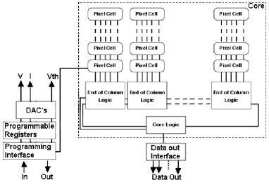
The mask and charge-injection registers consist of small size daisy chained flip-flop’s (FF’s) and are implemented in each pixel cell. A high logic level stored in one of the mask FF’s disables the corresponding cell. This is meant to turn off noisy cells. Analogously, a high logic level stored in one of the charge-injection FF’s enables the cell to receive at the input an analogue pulse for calibration purposes. Thus, there are two independent long registers, which are serpentine through the chip. The DAC registers control features of the chip and minimize the number of connections between the chip and the outside world. In the DAC’s the stored digital value is translated into an analogue voltage or analogue current to set bias voltages, bias currents and discriminator thresholds.
2.2 The preFPIX2 chip prototypes
The preFPIX2 represents the most advanced member of very successful succession of pixel readout chip prototypes [8]. It has been realized in standard 0.25m CMOS technology, following radiation tolerant design rules, from two vendors [9]. Last year exposures of preFPIX2T chips to radiation from a Colbalt-60 source at Argonne National Laboratory verified the high tolerance to gamma radiation up to about 33 MRad total dose [9]. In this paper, we present results of proton radiation tests performed with preFPIX2 chip prototypes including both total dose and single event effects.
The proton irradiation tests were performed exposing two chip prototypes, preFPIX2I and preFPIX2Tb chip, to 200 MeV proton beam at the Indiana University Cyclotron Facility (IUCF). The preFPIX2I chip, containing 16 columns with 32 rows of pixel cells and complete core readout architecture, was manufactured by a vendor through CERN. The preFPIX2Tb chip contains, in addition to the preFPIX2I chip features, a new programming interface and 14 8-bit DAC’s. It was manufactured by Taiwan Semiconductor Manufacturing Company. The comparison of the chip performance before and after exposure shows the high radiation tolerance of the design to protons up to about 43 MRad total dose. In addition, we measured the SEU cross section of static registers implemented on the preFPIX2Tb chip, in order to establish the sensitivity of our design to radiation induced digital soft errors during real operation.
3 Experimental setup
3.1 Proton irradiation facility at IUCF
The proton irradiation tests took place at the Indiana University Cyclotron Facility where a proton beam line of 200 MeV kinetic energy is delivered to users. The beam profile has been measured by exposing a photographic film. The beam spot, defined by the circular area where the flux is not less than 90% of the central value, had a diameter of about 15 mm, comfortably larger than the chip size (the larger chip is preFPIX2Tb which is 4.3 mm wide and 7.2 mm long). Before the exposure the absolute fluence was measured by a Faraday cup; during the exposure by a secondary electron emission monitor. The cyclotron has a duty cycle factor of 0.7% with a repetition rate of about 17MHz and most of the tests were done with a flux of about 21010 protons cm-2s-1. The irradiation was done with the chips powered on, in air at room temperature, and no low energy particle or neutron filters were used. The exposures with multiple boards were done placing the boards about 2 cm behind each other and with the chips facing the beam. Mechanically, the boards were kept in position by an open aluminium frame. The beam was centred on the chips. The physical position of the frame was monitored constantly by a video camera to ensure that no movements occurred during exposure. We irradiated 4 boards with preFPIXI chips to 26 MRad (December 2000), one board with preFPIX2Tb to 14 MRad (April 2001), and 4 boards with preFPIX2Tb to 29 MRad (August 2001). One of the boards with preFPIX2Tb chips on it was irradiated twice, collecting 43 MRad total dose. Due to the alignment precision and measurement technique employed, the systematic error on the integrated fluence is believed to be less than 10%.
3.1.1 LET spectra of 200 MeV protons in silicon
In reference [10] the production of ions in bulk silicon by a 200 MeV proton beam is described by a Monte Carlo simulation as a two stage process. In the first stage (internuclear cascade) the proton hits the silicon nucleus and produces light fragments, mainly forward. In the second stage the struck heavy ion (from nitrogen to silicon) recoils and evaporates isotropically producing further light fragments. In these inelastic collisions, the light fragments produced in the internuclear cascade, have a long range (up to more than 100 m) and low lineary energy transfer (less than 1.5 MeVcm2mg-1). The recoiling heavy ions have a shorter range (about 10 m) and relatively high lineary energy transfer (up to 14 MeVcm2mg-1) and can be very effective in causing SEU in electronics. In reference [11] the lineary energy transfer threshold for SEU in a static register realized in deep-submicron technology has been measured using ion beams of various species (i.e., various lineary energy transfer values) to be 14.7 MeVcm2mg-1. This value is quite high for a 0.25 m technology, but small enough to expect an SEU sensitivity to 200 MeV protons.
3.2 Hardware and software DAQ
Each chip under test was wire-bonded to a printed circuit board in such a way that it could be properly biased, controlled and read out by a DAQ system. The DAQ system was based on a PCI card designed at Fermilab (PCI Test Adapter Card) plugged in a PCIbus extender and controlled by a laptop PC. The PTA card generated digital signals to control and read back the readout chips. The software to control the PCI card IO busses was custom written in C. The PCI card busses were buffered by LVDS differential driver-receiver cards near the PCIbus extender located in the counting room. The differential card drove a 100 foot twisted pair cable followed by another LVDS differential driver-receiver card which finally was connected with a 10 foot flat cable to the devices under test. All the DAQ electronics were well behind thick concrete walls, protecting the apparatus from being influenced by the radiation background from the cyclotron and from activated material.
4 Experimental results
4.1 Single Event Latch-up
During the irradiation tests the circuits were powered with an applied bias voltage of 2.5V. The analogue and digital currents were continuously monitored via GPIB. The analogue current decreased slightly and the digital currents increased slightly during the proton exposure. No power supply trip-offs or large increases in the bias currents were observed during the irradiation. There is no evidence of single event latch-up or of significant radiation induced leakage currents. This result is expected from reference [11] where no evidence of latch-up up to linear energy transfer of 89 MeVcm2mg-1 was reported.
4.2 Single Event Gate Rupture
The damage of a CMOS device due to a Single Event Gate Rupture doesn’t necessary mean a hard failure of the chip but is likely to show up as performance degradation. In order to detect the occurance of SEGR due to the proton exposure, we measured the noise and the discriminator threshold of each individual cell before and after irradiation. The presence after exposure of a pixel cell with a noise or threshold significantly different from the other ones is an indication of radiation damage localized only in those particular cells, possibly the occurance of SEGR of individual transistors. So far we have completed the mentioned test for all four preFPIX2I boards, irradiated up to 26 MRad, and one of the preFPIX2Tb board, irradiated up to 43 MRad. We screened a total of about 2300 pixel front-end cells, each one containing about 550 transistors. All the cells were working before and after the irradiation, and none of them showed peculiar behavior. What has been observed after the irradiation has been a slight increase of the average threshold that can be adjusted by changing an internal bias-voltage reference (details about the FPIX2 front-end characterization after gamma and proton irradiation can be found in reference [12]).
Figures 2 and 3 show the threshold and noise distributions of a preFPIXI chip irradiated with a proton dose of 26 MRad. For these measurements the chip was biased exactly the same before and after irradiation except for the reference voltage of the second stage amplifier which was adjustted in order to have the same average threshold.
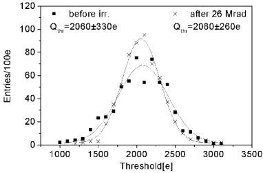
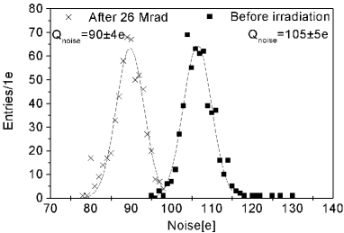
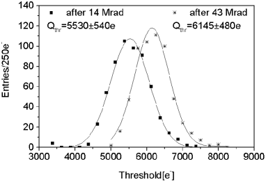
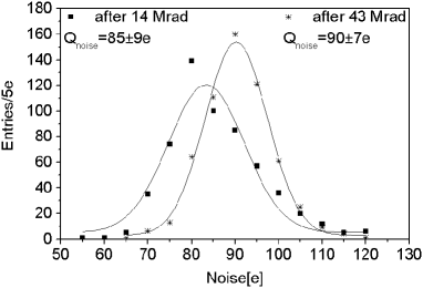
Figures 4 and 5 show the threshold and noise distributions of preFPIXTb chips irradiated with a proton dose of 14 and 43 MRad. For these measurements, the chips were downloaded with the same DAC values and a shift in the average threshold is clearly visible between 14 and 43 MRad total proton dose. The absence of noisy cells, and of large differences in individual thresholds due to irradiation, strongly suggest that single event gate rupture is not a concern in this design.
4.3 DAC analog response
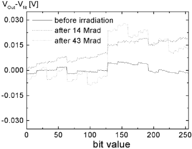
The analog output of the DAC’s implemented in preFPIX2Tb are available external to the chip. This means that change of the DAC behavior due to the proton irradiation can be measured. Figure 6 shows the response of the DAC used to adjust the discriminator thresholds before and after proton irradiation. The three curves shown correspond to the deviation from the linear fit for total doses of 0, 14, and 43 MRad. It is possible to see that the linearity and accuracy of the DAC output remain acceptable after 43 MRad total dose. The highest deviation from the linear fit is seen when the most significant bit is set true. In fact, the most significant bit has an associated current source drawing the same amount of current as all the other bits together, and a mismatch induced by the radiation shows up more in percentage. The spread could be quantified in terms of number of counts, and turn out that in the extreme situation of a total dose of 43 MRad, the digit inaccuracy is not more than 4 counts, where 255 counts is full scale. The behavior of the other DAC’s for high total dose is very similar to the one shown in Figure 6.
4.4 Single Event Upsets
In our tests, a great deal of attention was focused on measuring radiation-induced digital soft errors. We concentrated our effort on the preFPIX2Tb registers storing the initialization parameters, because they have a large number of bits and the testing procedure is easy to perform. The results obtained allow prediction of the performance of other parts of the chip potentially affected by the same phenomena.
4.4.1 Testing procedure
The single event upset tests performed are very similar to the ones reported in reference [11]. The SEU measurements consisted of detecting single bit errors in the values stored in the registers. The testing procedure consisted of repeatedly downloading all the registers and reading back the stored values after one minute. The download and read-back phases took about 3 seconds. The download of the parameters was done with a pattern with half of the stored bits having a logical value 0 and the other half having a logical value 1 (except in one case, see the caption in Table 1). For the shift-registers, the patterns were randomly generated at every iteration loop. For the DAC registers, the patterns were kept constant. A mismatch between the read-back value and the download value is interpreted as a single event upset due to the proton irradiation. No errors were observed in the system with the beam off and running for 10 hours.
In a separate test, the mask register of one board was operated in clocked mode with a clock frequency of 380 kHz. The low clock frequency value was due to our DAQ limitation. In this test, the mask register was downloaded with a logical level 1 in each flip-flop, in order to increase the statistics in view of the fact that a stored logical level 1 is easier to upset than a logical level 0 (see results). After the initialization, a continuous read cycle was performed and stopped every time a logical level 0 was detected. We collected 14 errors during an integrated fluence of 5.81013 protons cm-2.
A summary of the total single bit errors detected in the preFPIX2Tb readout chips, together with other relevant quantities, is shown in Table 1.
| Chip | Int. Fluence [ | Shift-Reg errors | DAC-Reg errors |
|---|---|---|---|
| 1 | 2.33 | 53=18()+35() | 10=8 ()+2() |
| 2 | 3.65 | 74=22()+52() | 19=9 ()+10() |
| 3 | 3.65 | 86=27()+59() | 19=8 ()+11() |
| 1 | 3.65 | 80=23()+57() | 20=8 ()+12() |
| 4 (450) | 3.65 | 77=14()+63() | 31=19()+12() |
One of the boards (indicated as board 4 in Table 1) was placed not orthogonal to the beam, as the other ones, but at 45 degrees to explore possible dependence of the error rate on the beam incident angle. The number of single bit upsets, for an equal amount of total dose, is statistically consistent among the various chips. In addition, the data do not show any statistically significant difference in the error rate between the tilted board and the others.
4.4.2 SEU cross section
It is common practice to express the error rate in a register as a single bit upset cross section , defined as the number of errors per bit per unit of integrated fluence:
| (1) |
where Nerrors is the number of upsets, F is the integrated fluence, and the number of bits exposed. The single bit upset cross section has been computed for the shift-registers and for the DAC registers. The results are shown in Table 2.
| Register | |
|---|---|
| Kill-Inject Mask () | 1.00.1 |
| Kill-Inject Mask () | 2.70.2 |
| Kill Mask () clocked at 0.38MHz | 4.21.2 |
| DAC | 5.50.6 |
Only the statistical error on the cross section has been considered. For the shift-registers, the cross section has been computed separately for the radiation induced transition from 0 to 1 and from 1 to 0 because the data have enough precision to show the existence of an asymmetry.
The high beam fluence used during the irradiation was of some concern regarding any saturation effect in the error rate. To study this, we collected some data at a fluence of about 4109 protons cm-2s-1, about 5 times less than the nominal fluence. In this short test, only one board was irradiated (Apr. ’01 test) and the single bit cross section was measured to be (1.41)10-16 cm2 and (3.51.6 )10-16 cm2 for the shift-registers and (75)10-16 cm2 for the DAC registers in un-clocked mode. This is statistically compatible with the results at higher fluence.
4.4.3 Discussion
The prediction of the single bit upset cross section is very difficult because a lot of parameters came into play [13]. Nevertheless, some gross features of the data can be understood simply by some general considerations. The disparity in the cross section between the shift registers and the DAC registers is likely caused by the different size of the active area of the NFET transistors, which are larger for the DAC register FF’s. Besides that, the DAC register FF’s have a more complicated design and an increase in complexity, as a rule of thumb, translates to a larger number of sensitive nodes that can be upset.
The SEU asymmetry for the transition from 0 to 1 with respect to 1 to 0 can be explained in terms of the FF design. The FF’s of the shift-registers are D-FF’s implemented as cross-coupled nor-not gates. Such a configuration has different sensitive nodes for 0 to 1 and 1 to 0 upsets. No such an asymmetry is expected for the DAC registers because the FF’s are D-FF’s implemented as cross-coupled nor-nor gates. This symmetric configuration has the distribution of sensitive nodes for low logical level the same as when a high logical level is stored.
A decrease of the energy threshold for single bit upset has been reported in reference [4] for a static register in clocked mode with respect to unclocked mode. Our data, taken with a clock frequency of 380 kHz, do not show a statistically significant difference from the data taken in the unclocked mode.
In reference [10] a beam angular dependence is expected for devices with very thin sensitive volumes that have linear energy transfer threshold over 1 MeV cm2mg-1 and tested with 200 MeV protons. We didn’t observe any dependence of the upset rate on the beam incident angle. In fact, due to the smaller device size of the deep submicron elements, the sensitive volumes are more cubic than slab shaped.
4.5 Impact of SEU on BTeV vertex detector
The vertex detector of BTeV consists of a planar array of 10 by 10 cm2 silicon pixel stations arranged perpendicular to the beam and siting inside a dipole magnet (about 1.6T). Each station is realized with two half L-shaped substrates staggered along z and covered by pixel sensors on both sides. The first measuring accurately one direction perpendicular to the beam (x), and the second the other direction (y). The elementary block forming the pixel detector is an assembly (module) of one long sensor with several readout chips bump bonded to it and a flex circuit cable which carries power and signal traces. The pixel sensor and the FPIX read out chips are the only active electronics parts on the module. The FPIX chips are controlled and read out by FPGA’s located outside the magnet. Thus, the FPIX chips are the only components which will be susceptible to soft (SEU) errors. Due to the long interaction region along the z direction (about 30 cm rms) most of the pixel detectors are crossed by particles coming from both directions. The insensitivity of the upset rate observed in our test with respect to the beam incident angle gives some confidence that the upset cross section doesn’t depend significantly on the direction of the incoming particle. Moreover, the recoiling ions causing upset in the electronics have a short range, so the material surrounding the readout chips is unlikely to generate secondary ions that can increase the upset rate. Nevertheless, in future tests we will measure the SEU cross section for beam incident on the backside of the chip and with chips bump bonded to sensors.
The vertex detector in BTeV is going to be exposed mostly to charged hadrons, neutrons, electrons and gammas coming from the interaction region. The particle flux of these species decreases as an inverse power of the radial distance (the neutron flux reachs a plateau just outside the vertex detector) and they have a broad energy spectrum up to about 100 GeV. The upset rate due to the electromagnetic component of the radiation field (gammas and electrons) can be neglected, because they produce few secondary ions in material. Table 3 shows the expected upset rate due to charged hadrons, high energy neutrons, and low energy neutrons for the different kinds of registers implemented in the FPIX2 chips. The cross section values used for the registers are the one measured in our tests and should represent very conservative estimates. In fact, the SEU upset cross section for protons saturates at about 200 MeV kinetic energy and is higher than the cross section for neutrons or pions for most of the energy spectrum involved. The data output serializer has not been implemented yet. Therefore, in this calculation, a register 24 bits long and a SEU cross section equal to 10-15cm2 are assumed for the serializer. We have to keep in mind that an increase in upset rate in the serializer can be expected when clocked at high frequency, but we don’t expect an intolerable rate of soft errors. The expected SEU bit error rate in the BTeV vertex detector is small enough that it will not be necessary to design explicitly SEU tolerant registers. We believe that the SEU rate can be confortably handled by a periodic readback of the chip configurations during the data taking and a re-download of the chip configuration when an upset is detected.
| Ch. Had. | n(E14 MeV) | n(E14 MeV) | |
|---|---|---|---|
| Flux [s-1plane-1] | 1.4 | 1.5 | 2.0 |
| Kill Reg. [bit h-1] | 10 | 1 | 1.4 |
| Inj. Reg. [bit h-1] | 27 | 2.7 | 3.8 |
| DAC Reg. [bit h-1] | 2 | 0.2 | 0.3 |
| Ser. Reg. [bit h-1] | 1 | 0.1 | 0.1 |
5 Conclusions
Total dose and single event tests validate the deep submicron CMOS-process FPIX2 designs as radiation tolerant, particularly suitable for exposure to large integrated total dose. No evidence of catastrophic failure or deterioration of the readout chip functionality has been observed up to dose up of 43 MRad (200 MeV protons). The single event upset cross sections of static registers are relatively small, but measurable (from 10-16 to 610-16 cm2). The expected SEU bit error rate in the BTeV vertex detector is manageable and does not require further SEU hardened registers to be implemented. Based on the experience gained from the gamma and proton irradiation, we intend to submit a full-size BTeV pixel readout chip before the end of the year 2001. That chip will include the final 50 micron by 400 micron pixel cells and a high speed output data serializer.
6 Acknowledgements
We thank Chuck Foster and Ken Murray for the generous technical and scientific assistance they provided us during the irradiation tests at IUCF. Fermilab is operated by Universities Research Association under contract with the US Department of Energy.
References
- [1] L. Adams, et al., 2nd RD49 Status Report: Study of the Radiation Tolerance of ICs for LHC, CERN/LHCC 99-8, LEB Status Report/RD49, 8 March 1999, available at http://rd49.web.cern.ch/RD49/Welcome.html#rd49docs.
- [2] A.H. Johnston, The Influence of VLSI Technology Evolution on Radiation-Induced Latchup in Space System, IEEE Trans. on Nucl. Sci., 43, 505 (1996).
- [3] F.W. Sexton, et al., Single Event Gate Rupture in Thin Gate Oxides, IEEE Trans. on Nucl. Sci., 44, 2345 (1997).
- [4] F. Faccio, et al., Single Event Effects in Static and Dynamic Registers in a 0.25 m CMOS Technology, IEEE Trans. on Nucl. Sci., 46, 1434 (1999).
- [5] M. Artuso, The BTeV pixel detector system, In these proceedings.
- [6] M. Wang, 1st level trigger for BTeV, In these proceedings.
- [7] A. Kulyavtsev et al., Proposal for an Experiment to measure Mixing, CP Violation, and Rare Decays in Charm and Beauty Particle Decays at Fermilab Collider(2000), http://www-btev.fanl.gov/public_documents/btev_proposal/
- [8] D.C. Christian, et al., Development of a pixel readout chip for BTeV, Nucl. Instrum. Meth. A 435, 144 (1999). D.C. Christian, A radiation-hard pixel readout chip for BTeV, Nucl. Instrum. Meth. A 473, 152 (2001).
- [9] A. Mekkaoui, J. Hoff, 30MRad(SiO2) radiation tolerant pixel front end for the BTeV experiment, Nucl. Instr. And Meth. A 465, 166 (2001).
- [10] P.M. O’Neill, et al., Internuclear Cascade - Evaporation Model for LET Spectra of 200 MeV Protons Used for Parts Testing, IEEE Trans. Nucl. Sci. 45, 2467 (1998).
- [11] P. Jarron, et al., Deep submicron CMOS technologies for the LHC experiments, Nucl. Phys. B (Proc. Suppl.) 78, 625 (1999).
- [12] J. Hoff, et al., Radiation tolerant circuits designed in 2 commercial 0.25m CMOS processes, FERMILAB-Conf-01/026-E, March 2001.
- [13] M. Huhtinen, F. Faccio, et al., Computational method to estimate Single Event Upset rates in accelerator environment, Nucl. Instr. And Meth. A 450, 155 (2000).