IEKP-KA/2001-20
Sept. 2001
Construction and Performance of a
Micro-Pattern Stereo Detector with
Two Gas Electron Multipliers
T. Barvich,
P. Blüm,
M. Erdmann,
M. Fahrer,
K. Kärcher,
F. Kühn,
D. Mörmann,
Th. Müller,
D. Neuberger,
F. Röderer,
H.J. Simonis,
A. Skiba,
W.H. Thümmel,
Th. Weiler,
S. Weselert
Institut für Experimentelle Kernphysik,
Universität Karlsruhe,
Wolfgang-Gaede-Str. 1, 76131 Karlsruhe, Germany
The construction of a micro-pattern gas detector of dimensions cm2 is described. Two gas electron multiplier foils (GEM) provide the internal amplification stages. A two-layer readout structure was used, manufactured in the same technology as the GEM foils. The strips of each layer cross at an effective crossing angle of degrees and have a m pitch. The performance of the detector has been evaluated in a muon beam at CERN using a silicon telescope as reference system. The position resolutions of two orthogonal coordinates are measured to be m and 1 mm, respectively. The muon detection efficiency for two-dimensional space points reaches .
Key words: detector, position sensitive, GEM, two-layer readout
PACS 29.40.Cs, 29.40.Gx
The authors would like to dedicate this work to
Siegfried Weseler
who unexpected died of a heart attack June 2001.
1 Introduction
Tracking of highly energetic particles which scatter under small angles in a strong axial magnetic field provides a prime challenge in future collider experiments. The trajectories of these so-called “forward particles” in the field require excellent measurements of the azimuthal coordinate along the tracks to precisely determine their momenta. For the simultaneous measurement of the radial coordinate only moderate precision is needed to determine their scattering angles with respect to the collision axis.
Gas micro-pattern detectors have been developed over many years for such applications. In particular, the small size readout pattern can handle high particle rates and provide good spatial resolution. Although these detectors were conceived for one-dimensional readout, two-dimensional readout has been made possible by introducing strips with a crossing angle or pads on the backside of the readout substrate [1]. This method however has serious problems associated with the low intensity of induced signals.
A new concept of two-dimensional readout was introduced by applying an etched Kapton111Kapton: Polymid film (Trademark of Du Pont). technology producing crossing strips on the readout side of the substrates [2]. The readout structure is kept at ground potential. Together with gas electron multipliers (GEM), developed by F. Sauli [3], such detectors can be produced at a reasonable cost and provide sufficient safety margin to be operated in a high rate environment [4].
2 Overview of the Detector Module
The module which is described here is a closed system of four trapezoidal detector units produced on a common board forming a segment of a ring (called the detector module) with the readout electronics and high voltage connections outside the contiguous gas volume of the detector. In between the readout structure and the drift cathode, two gas electron multipliers are inserted.
The separation of the readout stage and amplification stage allows the use of any appropriate readout pattern. While an orthogonal electrode system is considered as the optimum with respect to spatial resolution in both coordinates, it has the drawback of combinatorial ambiguities in case of multi-hit events. In order to optimize the detector for high rate capability and good resolution in the measurements of the particle momenta and scattering angles, a small crossing angle is chosen for the readout strips. The geometrical dimensions of the module have been chosen to correspond to the outer ring of the CMS forward tracker [5] in order to make as much use as possible of existing tools and equipment.
Figure 1 shows a schematic view of the detector module consisting of three gas gaps formed by frames supporting readout structure, GEM-foils, and drift cathode.
2.1 The Readout Structure
The coordinate information is extracted from the signals of strip electrodes produced on a 300 m thick glass fibre enforced epoxy board. The artwork for the readout structure was produced at CERN222A. Gandi, R. De Oliveira, CERN-EST-SM, Geneva, Switzerland. using the same technology as for the production of GEM foils. In a first step, the lower strip layer is produced by means of a lithographic method onto a copper-cladded board to which, in a second step, a single-sided copper-cladded 50 m thick Kapton foil is glued. Again by lithographic means the strips of the upper readout layer are patterned on that foil. Finally, the Kapton on top of the lower strips is removed by a chemical etching process, and the copper strips are gold plated.
The strips of the upper and lower readout layers cross at a relative angle of degrees. In order to minimize the crossing area and thus the capacitive coupling between the two layers, the strips are not made as straight lines but show a “steplike” shape producing up to 28 radially segmented readout pads (see Fig. 2). The widths of the strips are chosen to approximately equalize the charge sharing between the two readout planes resulting in upper strips that are 120 m wide and lower strips 240 m wide. The thickness of the copper strips is about 5 m. Each plane of the four detector units consists of 256 strips at a pitch of 406 m.
2.2 Gas Electron Multipliers (GEM)
The GEMs have been produced at the same CERN workshop as the readout structure. They consist of a 50 m thick Kapton foil, copper cladded on both sides. By lithographical methods and chemical etching, a regular hexagonal matrix of holes has been produced. The pitch of the holes is 120 m and the diameter is 80 m in the copper and about 45 m in the Kapton. Applying a voltage difference between both copper sides produces a dipole field high enough to provide gas amplification. Both copper sides have been etched into four electrically segmented units each corresponding in size to that of a readout unit.
2.3 Drift Cathode
The drift cathode is made of 360 m thick Ferrozell333Ferrozell GmbH, Augsburg, Germany. , a glass fibre enforced epoxy, on which a 20 nm thick layer of gold has been evaporated. Due to the low density of 1.75 g/cm3 the thickness corresponds to 250 m glass but with a much higher mechanical stability. The thermal expansion coefficient of Ferrozell (K-1 ) is comparable to that of Stesalit444Stesalit AG, Zullwill, Switzerland. (the material of the support frames) and so no thermal stress is expected.
2.4 Frames
The module frames are manufactured of Stesalit in the mechanical workshop of the IEKP Karlsruhe. Because of the small thickness of the drift cathode and the small cross section of the frames, an additional 2 mm top frame has been added to provide additional mechanical stability for supporting the GEM foils. The spacer frame between drift and upper GEM has a height of 3 mm. Between the two GEMs, and between the lower GEM and the readout plane, 2 mm spacer frames are used. The width of the frames is 3 mm. While the primary ionization volume of 3 mm thickness is typical to minimize the time of charge collection, the 2 mm transfer and induction gaps are optimized to separate the two amplification stages and to guarantee minimal charge diffusion.
3 Assembly
The mechanical assembly has to be done thoroughly to ensure a reliable performance of the detector. This requires careful quality control of all components, strict observance of high grade cleanliness during assembly, and dedicated tools which are briefly described in the following sections.
3.1 Quality Control
3.1.1 Readout Structure
In order to identify broken strips or shorts, the readout structure is tested by measuring the capacitance between neighbouring strips within each layer, and the capacitance of pairs of strips from the upper and lower layer which are neighbours on the bonding side of the structure. The measurement is performed on a fully automatic probestation which connects the individual pairs to a precision capacitance meter555Keithley 590 CV Analyzer..
Figure 3 shows the result of such a measurement for one individual readout unit. The capacitance values are reduced near the edges of the unit due to the trapezoidal shape of the readout structure resulting in shorter strip lengths on the non–parallel sides. The identification of a small defective region is evident in Fig. 3 where the presence of a short leads to increased capacitance values.
3.1.2 GEM-Foil
The quality control of the GEMs consists of an optical inspection and an electrical test for shorts between both copper sides. Moreover, the electrical insulation is tested in a dry nitrogen atmosphere up to 450 V. To reach this voltage difference a careful “training” procedure is followed. In particular the GEM is operated for 12 hours at 400 V. A leakage current of less than 20 nA at this setting is required for acceptance. As a result, 22 out of 24 delivered GEM foils were accepted.
3.2 Gluing the Module
Before mounting, all mechanical parts are cleaned in an ultrasonic bath with de-ionized water and dried in a laminar nitrogen flow cabinet. The GEM foils and the readout structure are thoroughly flushed with dry nitrogen immediately before gluing.
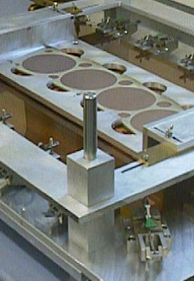
Since each GEM foil is supported only by the thin spacer frame, particular care is given to the assembly procedure of the drift cathode and the GEMs in order to provide enough stability to keep the GEM stretched. In a first step the drift cathode is glued simultaneously between top and spacer frame. After curing, this part together with the next spacer frame is glued to the first GEM foil which is stretched by means of a spring-loaded dedicated tool (see Fig.4).
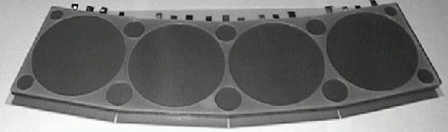
After curing, this step is repeated to glue the second GEM foil. Finally the readout board and the drift-GEM part are joined, closing the active volume of the detector module. All gluing is done using room temperature curing EPO-Tek 302666Polytec GmbH, Waldbronn, Germany.. Figure 5 shows the assembled module.
3.3 Connecting the Module
At distinct locations, the metallization of the GEM foils and of the drift cathode extends to the outside of the detector gas volume, forming the high voltage connection pads. After soldering thin high voltage cables to these pads, the remaining metallized structure is passivated by covering with a layer of epoxy to avoid discharges.
On the low voltage side, the readout strips are wire-bonded to a pitch adaptor reducing the effective 203 m pitch from the alternating strips of the two readout layers to the 44 m pitch of the front end chips.
The readout hybrid consists of a ceramic substrate with a set of 4 PreMux front end chips [6]. Each chip has 128 channels of charge preamplifiers, shaper-amplifiers and double-correlated sampling circuitry as well as an analogue multiplexer. The peaking time of the shaper was set at ns appropriate for high rate environments. One hybrid serves each of the four individual detector units. Together with an additional output buffer board, a single Flash-ADC channel is sufficient to readout the entire detector module.
The gas mixture is fed into the active detector volume through fan-outs integrated in the short sides of the frames. The gas flow was directed such that the GEM holes were flushed by the gas.
4 Detector Performance
The performance of the detector was examined in a high energy muon beam at CERN. The aims of the measurements were to
-
•
establish the region of optimal working parameters,
-
•
explore the detector characteristics in view of the stereo readout of the charges created in a single gas volume, and
-
•
examine the tracking quality where the criteria are the position resolutions, tracking efficiency and purity.
4.1 Experimental Setup
The experimental setup was situated in the X5 beam line of the CERN West area. A low intensity muon beam of energy GeV traversed a series of detectors placed on an optical bench. Events were triggered by a coincidence of two plastic scintillators of dimensions cm2 and cm2, respectively. A silicon telescope consisting of 4 double-sided detector layers with 50 m pitch, was used to measure two orthogonal coordinates [7]. The detectors have a sensitive area of cm2 and were positioned in two groups at a distance of 65 cm, allowing for precise predictions of the muon trajectories crossing the GEM detector. The position of the GEM detector was 90 cm behind the second silicon group. The detector was operated with Ar:CO2 in the ratio which we consider as a cheap gas mixture with no particular safety risks.
4.2 Analysis Tools and Definition of Observables
To analyse the responses of the detectors, the program package IRIS [8] was used and modified to our needs [9]. The program provides administration of the run-by-run pedestal and noise of each channel, and a clustering algorithm for the measured charge depositions. The cluster algorithm used considers channels with ADC values exceeding two standard deviations of the noise level. Starting at the channel with the maximum charge, all contributing neighbouring channels are grouped into candidate clusters. The main characteristics of the clustering algorithm are:
-
•
The signal charge of each cluster is calculated from the charge sum of all contributing strips in units of ADC counts.
-
•
The cluster position is provided by the charge weighted average position of the contributing strips in units of strip numbers.
-
•
The cluster size is given by the number of consecutive strips contained in the cluster.
-
•
As a measure of the cluster noise, the noise level of the channel with the maximum charge in the cluster is taken.
The program treats the cluster searches in both readout layers of the GEM detector separately.
As a measure of the relative gain we use the most probable value determined from fits of the Landau distribution to the data.
A further program, described in [10], was employed to measure the muon trajectories in the silicon telescope using the cluster candidates provided by the IRIS package. This program was used to align the detectors and to predict the muon positions on the GEM detector in order to measure the position resolution in the detector.
The program is further used to determine the tracking efficiency for single muons traversing the GEM detector,
| (1) |
Here is the number of muon tracks, and the nominator denotes the number of clusters in the detector which are associated with the predicted muon track within standard deviations of the measured position resolution.
The purity of the cluster measurements is determined from
| (2) |
In the denominator, all clusters are considered which overlap with the sensitive area of the silicon telescope.
4.3 Signal Distributions
4.3.1 Charge Distributions
Examples of charge distributions of the largest signal cluster in the event are shown in Fig. 6. The down-pointing triangle symbols represent the cluster charges measured in the lower readout layer. The distribution is found to approximately follow a Landau distribution. The corresponding fit is shown by the curve. The signal distribution of the upper readout layer is shown by the up-pointing triangle symbols together with the corresponding fit. This layer collects more charge carriers than the lower readout layer. Note that by construction the pad area of the lower layer is larger than that of the upper layer by a factor of , partially balancing the charge collection in the two layers. For this comparison, the small regions where the two readout layers cross have been excluded from the distributions. The circle symbols represent the event-by-event sum of the charges collected in both layers, and the curve gives the corresponding fit.
The charge relation of the two readout layers is further analysed in Fig. 7a. The box symbols represent the largest signal clusters found in the upper and lower readout layers. The distribution shows a strong correlation between the two signals together with a tail towards larger signals in the upper layer.
The histogram in Fig. 7b shows the charges collected in the upper readout layer while restricting the lower layer signals to the interval ADC units. The symbols show the charge measurements relating to events where the charge collection appeared within the region of the mm long pads. The tail towards larger signals in the upper readout layer therefore originates from the small regions where the strips of the two layers cross.
For charge collection within the pads, the signals of the upper readout layer are larger by a factor of compared to the lower readout layer as is shown in Fig. 7a by the symbols together with a linear fit to these values. The Gaussian fit of Fig. 7b gives a width of which demonstrates a strong charge correlation between the two layers.
In the region where the two layers cross, the signal of the upper layer is found to be a factor of above that of the lower layer (not separately shown in the figure).
4.3.2 Number of Strips Contributing to the Clusters
The spatial extent of the charge cloud collected on the readout layers gives additional information on the signal characteristics and the stability of the operating conditions. Examples of the number of strips contributing to the cluster with the largest signal in the event are shown in Fig. 8 as a function of the cluster charge . In Fig. 8a, the drift field was above kV/cm. The average cluster size (plotted as triangle symbols) varies between strips per layer and increases with , as expected from an increasing number of neighbouring channels exceeding the noise cut applied in our cluster finding algorithm. The dependence is compatible with a logarithmic increase of the mean cluster size with its signal charge and the curve shows the corresponding fit.
Below kV/cm (Fig. 8b), the number of strips contributing to the clusters are found to be much larger on average compared to the measurements above this drift field value. Since the same time delay relative to the trigger signal was used in all measurements, this effect presumably results from the electronics when the electron arrival times change with smaller drift velocities. In all following studies we therefore use the distribution of the cluster width as a criterion to ensure stable operating conditions.
4.4 Determination of the Working Parameters
In order to determine the optimal field strengths and to derive the corresponding signal in comparison to the noise level, field scans have been performed and analysed with respect to the cluster with the largest signal in each layer using the following conditions,
-
1.
The scans were analysed for detector regions with a uniform noise level of the contributing strips of about 15 ADC counts. This allows our cluster signal over single strip noise values to be converted to other definitions of the cluster noise.
-
2.
Events where the charges are collected in the crossing region of the two readout layers are excluded. The charges of the small fraction of signals from the crossing region can be derived with the information given above.
-
3.
To reject clusters not associated with muons traversing the detector, both readout layers have to show a signal cluster in the region covered by the beam.
In the case of the drift field scan, where the statistics have been relatively small owing to the cm2 scintillator used for triggering, only condition 1) was applied together with the requirement of a hit in one of the silicon layers in front of the GEM detector.
4.4.1 Scans of the Charge Collecting Fields
a) Drift Field. In Fig. 9, the drift field strength has been varied while fixing the strength of the other fields (kVcm, kVcm, V). The vertical axis represents the relative gain , measured in the lower readout layer. The inner error bars represent the statistical errors of the fits, the total errors include a conservative estimate of the uncertainty resulting from varying the binning and the region of the fits. The scale on the right axis gives the ratio of the relative gain divided by the average noise of a single channel contributing to the cluster.
The measurement exhibits a maximal at about kVcm. Here the signal over single strip noise is approximately . For values above kVcm, the signal is reduced. Simulations have shown that at high values of the drift field the proportion of the field lines ending on the upper GEM foil increases, leading to losses of primary electrons [11].
Instructive information on the region of low drift field values comes from Fig. 8 which was described in section 4.3.2. The open diamond symbols in Fig. 9 denote measurements with significantly larger cluster sizes compared to the other settings of the drift field. Although the relative gain is already large at kV/cm, stable operating conditions start at kV/cm.
b) Transfer Field. In Fig. 10, the relative gain is shown as a function of the transfer field, keeping the other fields fixed (kVcm, kVcm, V). In this figure the down/up pointing triangle symbols represent the signals measured in the lower/upper readout layers. The circles give the charge sum of the two layers. The solid line gives a guidance to the eye on the measurements of the lower readout layer. The transfer field leads to maximum charge values in the region of kVcm. The corresponding signal over single strip noise is around in the lower readout layer and in the upper layer respectively.
The dashed lines give the expected signals in the upper layer and the layer sum from the charge correlation discussed in Fig. 7. The good agreement of the upper layer measurements with this prediction shows that the charge correlation is a characteristic of the detector and is independent of the field values explored here.
The average cluster width was found to increase with the cluster charge at a similar rate as seen in Fig. 8a, implying good operating conditions for all measurements of the transfer field.
c) Induction Field. In Fig.11, the dependence of the relative gain is shown as a function of the induction field strength . The other fields remained fixed at kVcm, kVcm, and V. The signals increase with increasing , reaching a plateau for kVcm, with a signal over single strip noise ratio of about and in the lower and upper readout layers respectively. The measurements remain in this plateau, consistent with the field lines ending on the readout structure.
An analysis of the cluster widths showed much larger clusters, on average, at the lowest induction field value (open symbols) compared to all other measurements (full symbols). Good operating conditions were reached for kV/cm.
4.4.2 Scans of the Gas Electron Multiplier Fields
In Fig. 12, the dependence of the relative gain on the voltage applied to the two sides of the first GEM foil is shown by the solid symbols. The other fields were at kVcm, kVcm, kVcm, and V. The open symbols show the corresponding scan of the second GEM voltage, keeping V. The measurements exhibit a strong increase in dependence of the applied voltage as expected for gas electron amplification and the behaviour is the same when varying the first or second GEM voltage. To guide the eye, the solid curve represents an exponential fit to the lower readout layer measurements which was chosen to be quadratic in the GEM voltage to account for the large interval covered by the scans. The dashed curves are the predicted charge values for the upper layer and layer sum, according to the result of Fig. 7, which again illustrates the consistent behaviour of the charge sharing between the two readout layers.
The analysis of the cluster widths confirmed stable operating conditions at all field values under study.
4.5 Tracking Quality
To examine the tracking quality of the GEM detector, muon tracks were reconstructed in the silicon telescope and extrapolated to the surface of the GEM detector. For this analysis, runs with different gains were used, taking into account all clusters reconstructed in the upper and lower readout layers. After alignment of the detectors, the GEM detector was tested in two steps,
-
1.
First, the two readout layers were considered independently of each other, providing measurements of the coordinate perpendicular to the pads of the muons traversing the detector.
-
2.
Then combinations of the information of both layers were analysed. Of special interest are the sum and the difference of the position measurements. Owing to the small effective crossing angle of the two layers, the position sum gives an improved determination of the coordinate perpendicular to the pads. The difference in the positions provides a measure of the coordinate along the pads of the readout structure.
4.5.1 Spatial Resolution
Examples of the differences between the predicted muon tracks and the positions measured in the GEM detector are shown in Fig. 13. The precision reached for the single layer measurements is found to be m as determined by the Gaussian fits, and is improved to m when using both layers. This resolution compares well with the resolution obtained in detectors with one-dimensional readout of 200 m pitch [5].
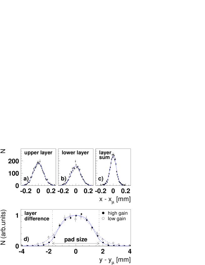
The resolution of the determined coordinate along the pads exhibits a broad plateau, owing to the pad size of mm being much larger compared to the extent of the charge cloud. Here two measurements are compared, where one was taken at high gain (solid circles), and the other at low gain (open circles). Both distributions have been fitted using a parameterization with exponential edges, showing a full width at half maximum of mm and shorter tails for the measurement with the larger signal clusters.
In Fig. 14, the dependence of the position resolution perpendicular to the pads on the relative gain of the clusters is shown, neglecting contributions from the finite resolution of the silicon telescope. The up/down pointing triangle symbols denote the upper/lower single layer information, and the circles give the result of the combined layer information. As expected, the position measurements are best at high gain.
The quality of the measurement of the coordinate along the mm long pads is shown in Fig. 15 as a function of the summed most probable signal-charge of the two layers. To give values comparable to the Gaussian widths shown in Fig. 14, we present here the width of the residual distribution containing 67 % of the detected events. We observe a resolution in the direction along the pads of mm.

4.5.2 Detection Efficiency and Rejection of Combinatorial Background
The efficiency, equation (1) in section 4.2, of detecting a muon track in the single layers and their combinations is shown in Fig. 16 as a function of the relative gain . The efficiencies reach for the upper/lower layer. The differences in efficiency can be attributed to the different fractions of the charge captured by in the two layers. Since both layer measurements are correlated due to the common primary ionization process, the combined measurements reach also efficiencies of .
To demonstrate the potential of rejecting “ghost hits” using the position and charge correlations between the two readout layers, the purity equation (2) is studied in Fig. 17 as a function of the relative gain . In Fig. 17a, the purity of the single layer measurement (triangle symbols) is shown to decrease with increasing cluster charge to the level of in the region overlapping with the silicon telescope. This is understood to arise from the increasing number of channels exceeding the noise threshold of the cluster definition.
Using the information of both layers provides an additional tool to reject the combinatorial ghost hits (Fig. 17b). Restricting the combinations to the area of the telescope and exploiting the charge correlation shown in Fig. 7 rejects most wrong combinations and background hits with insignificant losses of the efficiency.
5 Conclusion
We have presented the construction of a large micro pattern gas detector with a new two-layer readout design, optimized for forward particle detection in the endcap of a collider experiment, and suited to low-cost mass production. Using a high energy muon beam, we demonstrated that the detector is well operational under safe gas conditions over a wide range in the settings of the different electrical fields. The small effective crossing angle of degrees of the two readout layers, with m pitch each, allows one coordinate to be measured with m precision. In addition, the perpendicular coordinate can be determined with a precision of mm at a pad length of mm. The efficiency of detecting muons with the combined layer measurements has been determined to reach .
The performance tests give a significant part of the information required for applying the detector concept in a modern collider experiment. Although our detector has not been tested in a high intensity hadronic environment, we remark that micro-pattern gas detectors with GEM foils have been operated successfully under LHC equivalent conditions [5, 12].
Acknowledgements
For interesting comments and discussions we wish to thank G. Barker and S. Kappler. We thank our colleagues from the CERN accelerator devision for the successful operation of the muon test beam. For financial support we are grateful to the Bundesministerium für Bildung und Forschung (BMBF 05-HC8VK17). One of us (M.E.) wishes to thank Th. Müller and the IEKP group of the University Karlsruhe for their hospitality, and the Deutsche Forschungsgemeinschaft for the Heisenberg Fellowship.
References
- [1] F. Angelini et al., NIM A323 (1992) 531.
- [2] A. Bressan et al., NIM A425 (1999) 254.
- [3] F. Sauli et al., NIM A386 (1997) 531.
- [4] P. Blüm et al., Procs. of Int. Workshop on Micro-pattern Gas Detectors, Eds. M. Lemonnier and F. Sauli, Lure BP 34-91898, Orsay, France (1999).
- [5] M. Ageron et al., NIM A471 (2001) 380.
- [6] L.L. Jones, PreMux128 specification, Version 2.3, Rutherford Appleton Laboratory Internal Document, 1995.
- [7] L. Celano et al., NIM A381 (1996) 49.
- [8] Interactive Runfile Inspection System, following Diploma and PhD theses from M. Gottschalk, R. Ischebeck, J. Kremp, O. Pooth, D. Macke, A. Nowack, University Aachen (1999).
- [9] F. Kühn, Diploma Thesis, University Karlsruhe (2000).
- [10] W.H. Thümmel, PhD Thesis, University Karlsruhe (1999).
- [11] B. Zittel, Diploma Thesis, University Karlsruhe (1997).
- [12] S. Bachmann et al., NIM A470 (2001) 548.