DESY 01-117
August 22, 2001
Electromagnetic Radiation
Hardness of Diamond Detectors
T. Behnke a, M. Doucet a111Corresponding author,
N. Ghodbane a,
A. Imhof b, C. Martínez c,
W. Zeuner a
a DESY, Hamburg, Germany
b Universität Würzburg, Würzburg, Germany
c University of Portsmouth, Portsmouth, UK
Abstract
The behavior of artificially grown CVD diamond films under intense electromagnetic radiation has been studied. The properties of irradiated diamond samples have been investigated using the method of thermally stimulated current and by studying their charge collection properties. Diamonds have been found to remain unaffected after doses of 6.8 MGy of 10 keV photons and 10 MGy of MeV-range photons. This observation makes diamond an attractive detector material for a calorimeter in the very forward region of the proposed TESLA detector.
(To be submitted to Nucl. Instr. and Meth.)
1 Introduction
Diamond has been extensively studied in recent years for use for particle detection [1]. Many studies have focused on the hadronic radiation hardness properties of diamond for applications at the LHC. Diamond detectors have been shown to remain undamaged up to fluences of neutrons, protons and pions of the order of /cm2 [2]. On the other hand, diamonds have only been tested with electromagnetic doses of up to 0.1 MGy [3]. Electromagnetic radiation hardness is a very important issue for low-angle detectors for the TESLA linear accelerator project [4]. A luminosity calorimeter, which would serve both as a fast luminosity monitor [5] and as a low-angle calorimeter, is planned for this project. According to the current design, this detector would be placed only 1.2 cm from the beam line. A very large beam-induced background of photons and electrons would deposit a dose of as much as 1 MGy per year in the detector elements closest to the beam. Given these very large doses and the resistance of diamond to hadronic radiation, diamond has been considered as a potential detector material. Silicon detectors have also been shown to operate after having received doses of several MGy of electromagnetic radiation [6] and could also be considered as active material for this detector. This paper addresses the electromagnetic radiation hardness properties of diamond up to doses comparable to several years of TESLA running. Collection distance measurements and thermally stimulated current measurements (TSC) were conducted using diamonds irradiated by a 10 keV photon beam. Collection distance measurements were also performed with a diamond irradiated by a 60Co source (emitting with 0.32 MeV endpoint and photons of 1.17 MeV and 1.33 MeV).
2 Principle of operation
Artificially grown CVD diamond has already been demonstrated to be a good semi-conductor detector material [1]. A voltage is applied between two electrical contacts made on each side of a thin diamond film, typically of the order of 300-500 m thick. The energy deposited by passing charged particles creates electron-hole pairs which induce a charge on the contacts as they migrate towards them. The band-gap of diamond is 5.5 eV, and 13 eV is on average needed to create an electron-hole pair.
Due to impurities in the diamond, the migrating charges can be trapped on their way towards the electrical contacts. The charge induced on the contacts is then smaller than the total charge created in the diamond. The collection efficiency , is defined as
| (1) |
where is the charge induced on the contacts and corresponds to the charge of the total number of electrons released in the diamond by the ionization process. The collection distance, representing the average distance between the electron and the hole of a given pair at the moment when they are stopped, is related to the collection efficiency by
| (2) |
where is the thickness of the detector [1]. For CVD diamonds, the collection distance is usually significantly shorter than the thickness of the detector (up to about 2/3 of its thickness). Being intimately linked to the performance of the detector, the collection distance is used as a figure of merit of the diamond material.
The collection distance is influenced by the applied voltage. Since the mobility of charge carriers depends on the applied voltage, the collection distance will in turn depend on the voltage. It reaches an asymptotic value at a voltage corresponding to the saturation point of the mobility. In the following, we will always refer to the asymptotic value of the collection distance, reached at a typical voltage of 1 V/m.
The collection distance is affected by the amount of radiation the detector has previously received, through the so-called priming effect [7]. As the diamond is irradiated, the charges created in the material are partially trapped in energy levels that are created by impurities. Although short-lived defects can be expected to rapidly release the trapped charges and be available for trapping at a later time, long-lived defects can remain filled long enough to be unavailable for further trapping on the time-scale of the measurement. Such long-lived defects have been observed in diamond using the method of thermally stimulated current [8, 9, 10, 11]. The priming effect decreases the effective number of trap energy levels and the collection distance consequently increases. This effect reaches saturation once all long-lived traps have been filled. In the following, we will always refer to the collection distance of primed diamonds.
3 Thermally stimulated current measurements
The energy and the amount of trap levels in the diamond can be measured with the method of thermally stimulated current [12]. A voltage is applied between contacts on both sides of the diamond. One of the two contacts is grounded and is used to measure the current flowing through the material. After a short irradiation period to fill traps, the diamond is heated up. As the temperature of the diamond rises, trapped charges are thermodynamically released at a rate depending on the temperature and on the energy level of the traps. A current proportional to the trap density and to the release rate is then observed between the contacts of the diamond sample. As the temperature rises, the release rate increases until no charge is left to be released. For large enough temperature, the rate of electrons in the valence band of the diamond thermodynamically crossing the band-gap can be sufficient to create a large current. This current is increasing with the temperature and constitutes a background to the TSC from released traps.
The TSC dependence on the temperature gives information on the energy levels and the density of the impurities in the diamond. Since the measured current corresponds to a rate of release, the heating rate of the diamond also has to be known to extract this information.
In the present TSC measurements, a sizeable portion of the TSC comes from the background current at large temperature. This translates into a large error on the background subtraction. For this reason, only the TSC peak maximum, for which the background contribution is smaller than at higher temperature, has been used for comparing the diamond behavior after various doses of radiation. A fit to the TSC curves has also been done to extract the energy level of the TSC peak and verify the quality of the data.
Assuming that released traps have a negligible probability of being recaptured, the TSC can be written as follows [13]:
| (3) |
where is the TSC, is the initial number of trapped carriers, the energy level of the trap, a frequency factor, the initial temperature, the absolute temperature, the Boltzmann constant and the heating rate.
4 Experimental procedures
The Hasylab facility at DESY provides photon beams from synchrotron radiation. A 10 keV photon beam [15] was used to expose two diamond samples to large electromagnetic radiation doses. The average irradiation rate was calculated to be approximately equal to 14 Gy/s. To test the resistance of the diamond samples to radiation, two types of measurements were performed before and after the irradiation periods. The collection distance of each sample was measured and a set of TSC measurements was performed. During the TSC measurements, the Hasylab beam was also used to create electron-hole pairs in the sample under study. To verify the resistance to radiation from photons having a higher energy, a 60Co source was also used to irradiate a third diamond sample.
The collection distance was evaluated by measuring the total charge induced on the contacts of the sample by electrons from a 90Sr source. A signal from a Si-detector placed behind the diamond detector provided a trigger. For each trigger, the diamond detector was read out using an Amptek A250 222AmpTek Electronics pre-amplifier, that was followed by an Ortec amplifier/shaper with 3 s shaping time. Both the Si-detector and diamond signals were read out by a digital oscilloscope. The collection distance is related to the measured signal left by single electrons by the following relation:
| (6) |
where is the total measured charge, corresponds to the predicted charge of the total number of electrons released by the ionization process of a single incident electron and is the thickness of the diamond. The measurements were carried out after having primed the diamonds, at a voltage corresponding to the maximum carrier velocity.
To measure the TSC, a nominal voltage of -50 V was applied on one contact of the diamond during measurements and irradiation periods. The other contact was connected to a Keithley 6514 333Keithley Instruments GmbH to measure the current. To generate the thermally stimulated current, a remote-controlled heating element was used. The heating rate of this element was measured to be K/s. The temperature was monitored using a thermocouple element read by a voltmeter. During the acquisition sequence, the temperature and the current were measured at two second intervals. To reduce the time between TSC measurements, liquid nitrogen was used to cool the heating element to ambient temperature once the maximum temperature was reached.
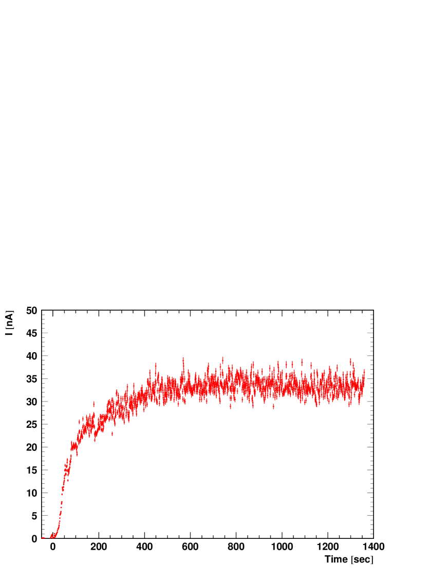
Before heating the diamond, a fixed period of irradiation was used to create electron-hole pairs in the diamond and fill traps. For this purpose, the 10 keV photon beam of Hasylab was directed on a slit. A remote-controlled shutter was placed between the detector and the slit to switch the beam on and off between data taking periods. To monitor the photon beam, a scintillator read out by a photomultiplier was placed near the beam to measure the electrons produced by the scattering of beam photons with air. For each acquisition sequence, an irradiation period of 60 seconds was done before the TSC curve was recorded, corresponding to approximately 840 Gy. Figure 1 shows the current measured on one contact of the diamond during an irradiation period of more than 20 minutes. The current rises as traps in the diamond are filled and reaches a maximum after about 10 minutes ( kGy). The 60 second irradiation time used is therefore well below the time period over which saturation effects are visible.
Three diamonds of similar properties were used for three sets of measurements. All three were produced by DeBeers 444DeBeers Industrial Diamond Division. They have a thickness of 300 m and an average grain size of approximately 20 m. Contacts were deposited on both sides of each sample 555The contacts were done by the Fraunhofer Institut für Schicht und Oberflächentechnik, Braunschweig, Germany. They consist of depositions of Ti (50 nm), Pt (30 nm) and Au (60 nm).
One diamond (denoted diamond #1) was used to perform a surface scan of TSC measurements. A region of about 1 mm2 in steps of was measured before irradiation and after doses of about 0.2 MGy and 1.4 MGy.
A second diamond (#2) was used in a test involving larger doses. TSC measurements were performed at various voltage values before irradiation and after doses of about 1.4 MGy and 5.4 MGy. For these measurements, the full surface of the diamond was irradiated. For both diamonds (#1 and #2), the collection distance was measured before irradiation and after the last irradiation.
A third diamond (#3) was sent for irradiation at a 60Co source 666Gamma-Service Produktbestrahlung GmbH. The collection distance of the diamond was also measured before irradiation and after doses of 1 MGy and 10 MGy. A 60Co emits photons of 1.17 MeV and 1.33 MeV, which are above the threshold for non-ionizing damages. It is therefore interesting to compare the effects of low energy and high energy photon radiation.
5 TSC signal treatment
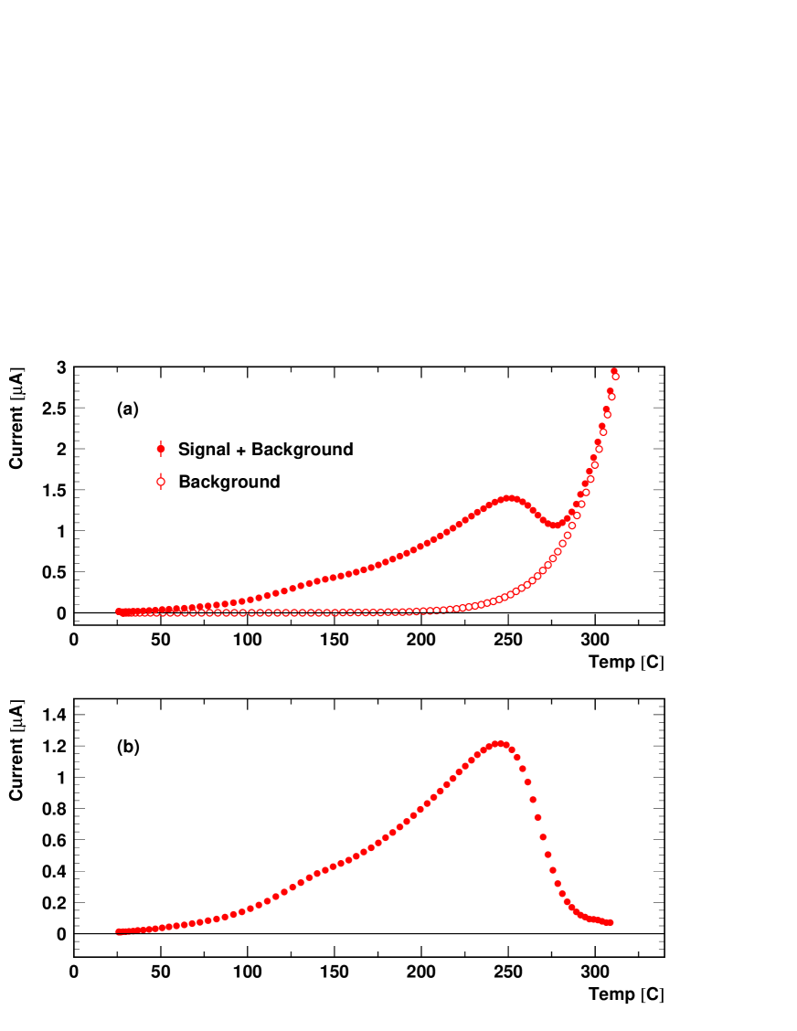
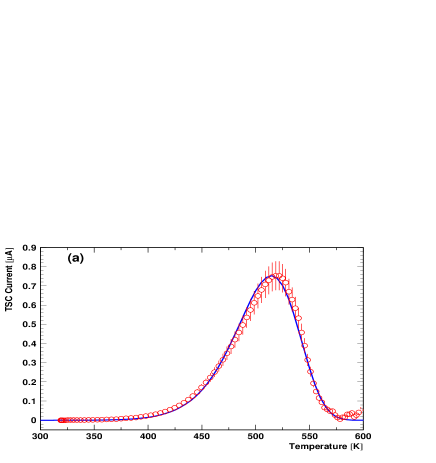
Figure 2a shows an example of a TSC signal measured with diamond #1 during the surface scan. The peak at 250 ∘C corresponds to the TSC peak from released charges. The background current described in Section 3 can be seen at higher temperature and must be subtracted to obtain the part of the current due to the trap release. The open points on Figure 2a show a background curve obtained in a subsequent run without irradiation. For each TSC curve of the scan performed with diamond #1, the signal was extracted by subtracting the same background curve. Figure 2b shows the signal extracted from Figure 2a.
In order to verify the background subtraction technique and to estimate the systematic errors, each scan was subdivided in four small raster scans of with overlapping regions. The overlapping points, taken at different times, were compared and the RMS of the distribution of the difference between the measurements was taken as the systematic error. A systematic error of 12% was found. This error includes the effect of the flux variations, for which no correction was applied for this evaluation.
For the TSC data taken with diamond #2 (for which the complete surface of the diamond was irradiated), the background subtraction scheme was different. Due to the large irradiated surface, the TSC signals were very large. The background was changing according to the voltage applied, which was varied between 5 V and 150 V. A fifth degree polynomial was fitted on each side of the TSC peak to estimate the background value at the peak maximum. The results obtained with this technique were checked by comparing to background curves taken at 50 V. A conservative error equal to the fitted background current, corresponding to about 8% of the TSC peak, was added to the 12% systematic uncertainty mentioned earlier. The total error on the TSC peak is taken to be 15%.
Although the background remains the same for all TSC curves taken at a given voltage, the signal depends on the photon beam flux. In order to apply a correction for the beam flux, a scintillation counter was placed near the beam to count beam-air interactions. Figure 3 shows the correlation between the maximum TSC and the beam flux for the three scans of diamond #1. If no flux variation were present, no correlation between the two should be visible. A linear fit to the points is also shown. A linear flux dependence of the TSC signal is justified by the short irradiation period of 60 seconds. In such a short time, no saturation effect of the trap filling is expected (see Figure 1). This linear relation was used to correct the TSC signal to a single photon flux value. The systematic error corresponding to the flux correction is included in the 12% uncertainty mentioned above.
6 Extraction of energy levels and trap density
A fit to the TSC curves was performed to evaluate the energy level of the traps. The large sample of curves from the TSC scan was also used to evaluate the systematic error on this measurement. The comparison of the results to previously published data [8, 9, 10, 11] provides a cross-check of the quality of the TSC measurements.
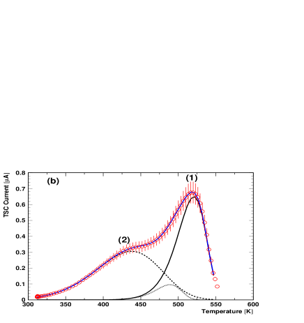
Figures 8a and 8b show two examples of TSC curves and the associated fits using Equation 4. The two curves correspond to diamond #1, with an irradiated area of . The data shown on Figure 8a were fitted using a single TSC peak, while a superimposition of three TSC peaks was fitted to the data shown on Figure 8b. For Figure 8a, an energy level equal to eV was found. The systematic error on all fitted parameters was estimated using the discrepancy between several measurements. The quality of the fit is estimated with the figure of merit (FOM) of Balian and Eddy [16], in the present case equal to . Using Equation (5), one gets a frequency factor GHz. On Figure 8b, one can clearly notice the presence of two trap energy levels fitted at eV for the most intense and eV for the second one. The FOM for this fit is equal to . Using all TSC curves from diamond #1, an average energy of eV was measured for the peak at 250 ∘C and eV was measured for the peak at around 150 ∘C.
Different energy levels of defects found in CVD diamond samples are reported in the literature. Two energy ranges have been observed, one below 1 eV (0.5 eV [8], 0.87 eV [10] and 0.8 eV [11]) and one above 1 eV (1.8 eV [8], 1.86 eV [9] and 1.42 eV [10]). Our results are compatible with the low energy levels previously observed.
7 Radiation hardness results
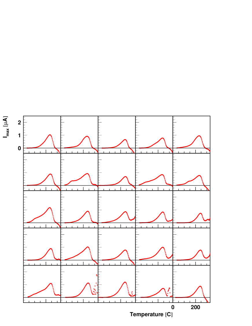
A surface of approximately 1 mm2 of diamond was scanned in steps of . A TSC measurement was performed at each position. The background subtraction and the photon flux correction were applied to the measured signal. Three scans were performed: before irradiation, after a dose of 0.2 MGy and after a dose of 1.4 MGy. Due to time constraints, a surface of only 0.5 mm2 was scanned after the last dose. The surface scanned was not the same for all scans. Figure 4 shows an example of a TSC scan. The figure shows TSC curves after background subtraction. These data were taken before irradiation. One can see variations in the background, leading to the 12% systematic error on the peak measurement mentioned in Section 5. Some large fluctuations are also seen at large temperatures, above the TSC peak. These fluctuations do not cause problems in the analysis. It is also interesting to note that in some cases, what appears to be a second small peak at around 150 ∘C is also observed. This could be due to the presence of an additional trap level. Given the size of these peaks and the fact that they do not appear at every scanned position, they were not used for testing radiation hardness. An example of such a peak has been discussed in Section 6.
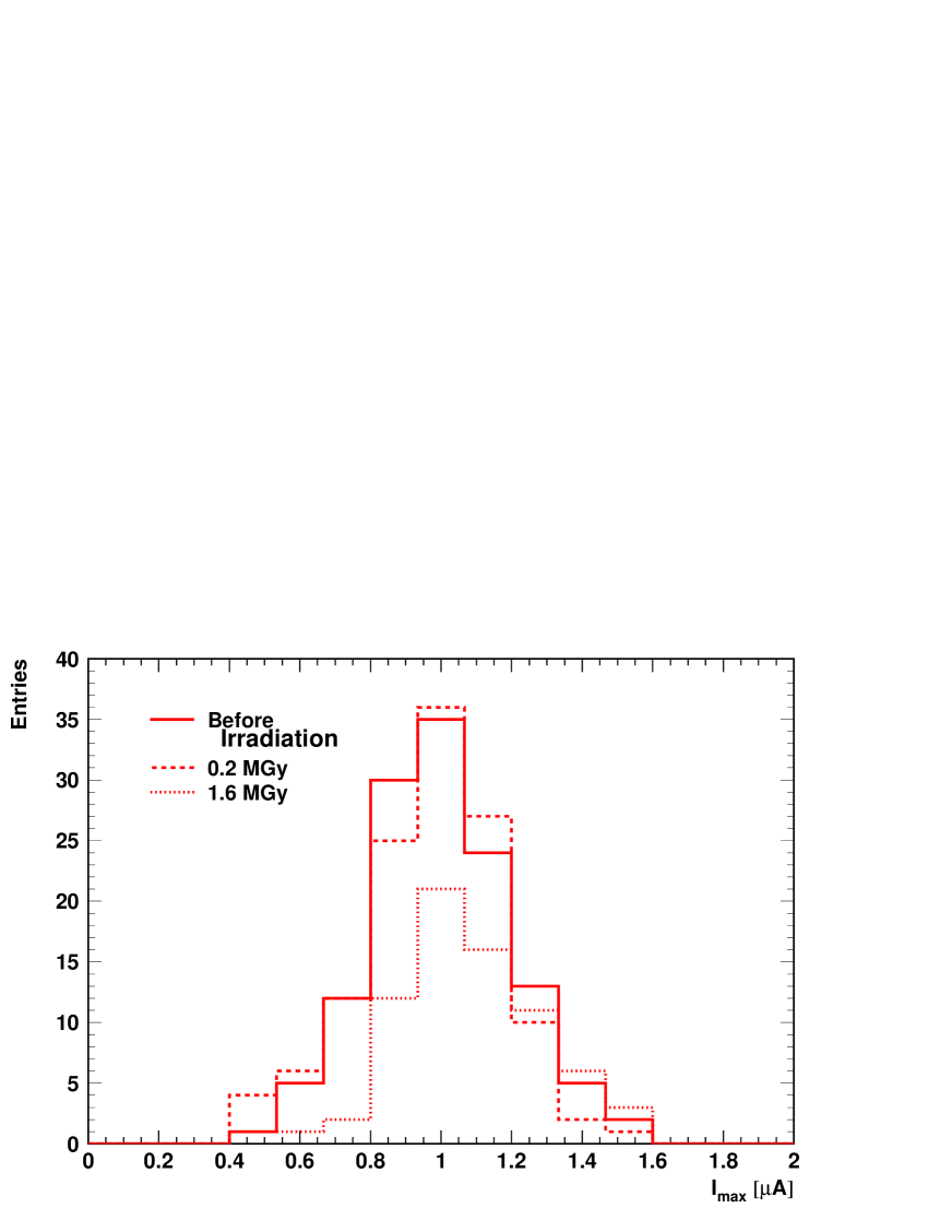
Figure 5 shows the distribution of , the current at the TSC peak, for each scan. No effect on the TSC peak distribution as a function of the radiation dose was observed. The RMS/mean values obtained for the different doses are: 0.2/1.0, 0.2/0.97 and 0.21/1.1. The distribution of points is therefore a little wider than the systematic error, although not significantly. Since the CVD diamond material is made of a large number of small crystals having several tens of microns in lateral size, the measured signal is an average over several crystals. For this reason, the measurement is not sensitive to the granularity of the material.
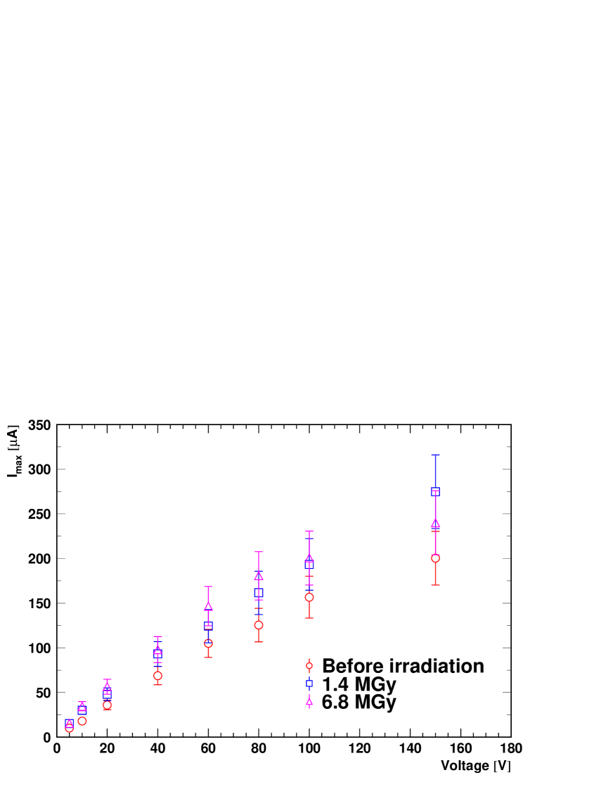
The full surface of a second diamond (#2) was irradiated in two consecutive steps of 1.4 MGy and 5.4 MGy. TSC measurements were performed before irradiation and after each exposition to the beam. TSC curves were taken for different voltages. The TSC peaks obtained were corrected for background and photon flux and are shown in Figure 6. The rising behavior of the TSC peak as a function of the applied voltage corresponds to the increasing mobility for higher voltages. A good agreement between data points taken after different doses of irradiation is observed.
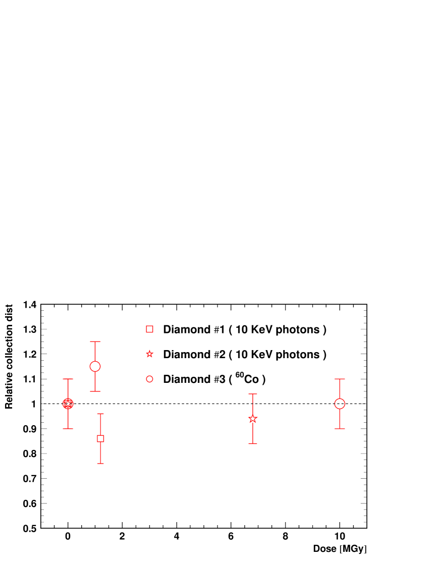
Table 1 shows the collection distance measurements performed on the different diamond samples for various doses. The ratio of the collection distance measured after irradiation to the collection distance measured before irradiation is shown in Figure 7 for each diamond and each irradiation period. In the case of diamonds #1 and #2, which were used for the Hasylab measurements, the collection distance was measured before the TSC scans and after the last irradiation. Diamond #3 was measured before and after being sent to a 60Co irradiation facility. The errors on the collection distances are mainly systematic and represent the reproducibility of the measurements. They were estimated at 10% for each measurement, by comparing several measurements recorded at different times. Several thousand data points, each corresponding to the passage of a single minimum ionizing particle, were taken for each measurement, so that the statistical error is negligible compared to the systematic error. Although diamond #3 shows large variations in its collection distance, no evidence for defects due to radiation was observed.
| Sample | Dose (MGy) | energy | Coll. distance (m) |
| #1 | 0 | – | |
| #1 | 1.6 | 10 keV | |
| #2 * | 0 | – | |
| #2 | 6.8 | 10 keV | |
| #3 | 0 | – | |
| #3 | 1 | 1.17 & 1.33 MeV | |
| #3 | 10 | 1.17 & 1.33 MeV |
In summary, the collection distance measurements and the TSC measurements show no indication of a degradation of the diamond quality as a function of the radiation dose. The collection distance remains constant within errors up to at least 10 MGy and the TSC peak, which is indicative of the energy and the number of traps in the material, remains stable up to at least 6.8 MGy.
8 Conclusions
CVD diamond films were submitted to large electromagnetic radiation doses. A surface scan of thermally stimulated current measurements was performed to test the stability of the trap level density after various irradiation doses. The collection distance of these diamond samples was also measured before and after these irradiation periods. The properties of the diamonds were found to remain unchanged after irradiation doses of up to 6.8 MGy of 10 keV photons and of up to 10 MGy of photons with 1.17 MeV and 1.33 MeV. Such a resistance to electromagnetic radiation justifies the use of diamond as material for future detectors such as the low-angle calorimeter of TESLA.
Acknowledgements
We would like to thank the staff of Hasylab for hosting us for the duration of our experiment. A special thanks to C. Paulmann who was responsible for the experimental area and to G. Kitis and P. Gonon for discussions on the TSC analysis. We would also like to thank A. Oh for his help.
References
- [1] W. Adam et al., Review of Development of Diamond Radiation Sensors. In Proceedings of International Workshop on GaAs and Related Compounds, Praha-Pruhonice, 1998. D. Meier, Diamond Detectors for Particle Detection and Tracking, PhD thesis, Universität Heidelberg, 1999. A. Oh, Particle Detection with CVD Diamond, PhD thesis, Universität Hamburg, 1999.
- [2] W. Adam et al., Performance of Irradiated CVD Diamond Micro-Strip Sensors. In Proceedings of Int. Conf. Rad. Eff. on Semicond. and Mat., Florence, Italy, 2000. A. Oh, M. Moll, A. Wagner and W. Zeuner, Diamond and related materials, 9(11) (2000) 1897.
- [3] RD42 Collaboration, C. Bauer et al., Nucl. Instr. Meth. A367 (1995) 202.
- [4] TESLA Technical Design Report, Part IV: A Detector for TESLA, editors: T.Behnke, S. Bertolucci, R.-D. Heuer, R. Settles, 2001.
- [5] O. Napoly and D. Schulte, Luminosity Monitor Options for TESLA. In Proceedings of XIX International Linear Accelerator Conference, LINAC 98, Chicago, IL, USA, 1998.
- [6] G. Lindström et al., Nucl. Instr. Meth. A466 (2001) 308.
- [7] T. Behnke et al., Nucl. Instr. Meth. A414 (1998) 340. T. Behnke et al., Diam. Rel. Mat. 7 (1998) 1553.
- [8] C. Bowlt, J. Phys. D: Appl. Phys., 6 (1973) 616.
- [9] P. Gonon, S. Prawer and D. Jamieson, Appl. Phys. Lett. 70(22) (1997) 2996.
- [10] D. Tromson et al., Phys. Stat. Sol. (a) 174 (1999) 155.
- [11] D. Briand et al., Diam. Rel. Mat. 9 (2000) 1245.
- [12] M.G. Buehler, Solid-State Electronics 15 (1972) 69.
- [13] S.W.S. McKeever, Thermo-luminescence of solids, editors: R.W. Cahn, E.A. Davis and I.M. Ward, Cambridge University Press, 1985.
- [14] G. Kitis, J.M. Gomez-Ros and J.W.N. Tuyn, Thermo-luminescence glow-curve deconvolution functions for first, second and general orders of kinetics, J. Phys. D31 (1998) 2636.
- [15] K. Fischer, H.-G. Krane, W. Morgenroth, Nucl. Instr. Meth. A369 (1996) 306.
- [16] H.G. Balian and N.W. Eddy, Nucl. Instr. Meth. 145 (1977) 389.
 |
 |