Performance of prototype BTeV silicon pixel detectors in a high energy pion beam
Abstract
The silicon pixel vertex detector is a key element of the BTeV spectrometer. Sensors bump-bonded to prototype front-end devices were tested in a high energy pion beam at Fermilab. The spatial resolution and occupancies as a function of the pion incident angle were measured for various sensor-readout combinations. The data are compared with predictions from our Monte Carlo simulation and very good agreement is found.
keywords:
BTeV, beam test, calibration, pixel, silicon, resolution.PACS:
29.40.Wk , 29.40.Gx , 29.50.+V, , , , , , , , , , , , , , , , , , , , , , , and ††thanks: Corresponding Author: e-mail:artuso@physics.syr.edu
1 Introduction
BTeV is an experiment expected to run in the new Tevatron C0 interaction region at Fermilab in 2006. It is designed to perform precision studies of and quark decays, with particular emphasis on mixing, CP violation, rare and forbidden decays [1]. This experiment takes advantage of two important features of the “forward” region: the correlation in the direction of the produced and , that improves the flavor tagging efficiency, and the boost that is exploited in our trigger algorithm based upon the identification of detached charm and beauty decay vertices. The unique feature of BTeV is that this algorithm is implemented in the first trigger level [2]. Consequently, the vertex detector must have a fast readout, superior pattern recognition power, small track extrapolation errors, and good performance even after high radiation dose. Silicon pixel sensors were chosen because they provide very accurate space point information and have intrinsically low noise and high radiation hardness.
In this paper we report the results of the 1999-2000 BTeV silicon pixel detector beam test and we compare them to Monte Carlo predictions. The beam test was carried out at Fermilab in a 227 GeV/c pion test beam. The pixel detectors tested were hybrid assemblies of several combinations of pixel readout chip prototypes developed at Fermilab, and single-chip sensor prototypes. The main goal of our studies was to measure the spatial resolution attainable along the short pixel dimension for different sensor technologies and for different readout electronics configurations. In particular, we have performed an extensive investigation of the effects of varying the discriminator threshold and the front-end device digitization precision.
2 Experimental setup
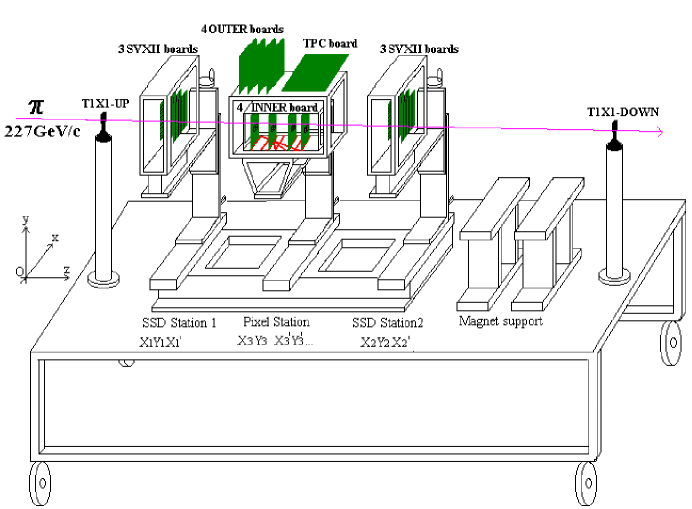
The data were collected at the MTest beam line located in the Meson Area at Fermilab. Fig. 1 shows the experimental set-up. The pixel devices were located between two stations of silicon microstrip detectors (SSD’s) that provided tracking information to an accuracy of about 2 m in the direction, corresponding to the “small pixel dimension” (50 m). The pixel hybrid devices were mounted on printed circuits boards, held inside an aluminum box, where their location was determined by precision machined slots. One of the pixel devices in the telescope could be positioned in slots at various angles with respect to the beam direction. This enabled us to measure the properties of various pixel prototypes as a function of the pion incident angle.
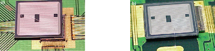
The pixel detectors tested are all from the “ATLAS prototype submission” [3], and all have 50 m 400 m pixels. They use the technology, with the pixel electrodes located on the ohmic side of the device. In order to achieve good inter-pixel insulation, two approaches have been tried. The “-stop” technique uses implants between the pixel cells, deposited through a mask with the chosen implant geometry, whereas in the “-spray” technique, pixel implants are deposited after a shallow layer is deposited uniformly throughout the active area. Two of the sensors were produced by CiS, Germany, and the other three by SII, Japan. Fig. 2 on the left shows an FPIX0 bonded to the CiS -stop sensor. The instrumented portion of the sensor is 11 columns 64 rows. The CiS sensors (one -stop ST1 and one -spray ST2) were indium bump bonded to FPIX0 readout chips by Boeing North America, Inc. The SII sensors (two -stop ST1’s and one -spray ST2) were indium bump bonded to FPIX1 readout chips by Advanced Interconnect Technology Ltd. (AIT, Hong Kong). The depletion voltage, measured through the dependence of the leakage current on the reverse bias applied, is 85 V for the CiS sensors and 45V for the SII sensors. The sensor thickness was about 300m.
The front-end device to be coupled to the pixel sensors must satisfy several challenging requirements. In order to obtain the optimal spatial resolution achievable with the chosen pitch, analog information is needed. On the other hand, it is necessary to transfer the hit information very quickly to the trigger processor in order to be able to use it in the first trigger level algorithm. The development effort towards the final chip [5] has proceeded along several steps of increasing complexity.
The first iteration, FPIX0, has 12 columns of 64 rows. Each FPIX0 readout pixel contains an amplifier, a comparator, and a peak sensing circuit. When any comparator fires, a FAST-OR signal is asserted. FPIX0 provides a zero-suppressed readout of hit pixels. The information read out consists of hit row and column numbers, together with a voltage level which is proportional to the peak pulse height. For these measurements, the analog output was digitized by an external 8-bit flash ADC.
FPIX1 is the second-generation pixel readout chip developed at Fermilab, and is the first implementation of a high speed readout architecture. Each FPIX1 cell includes 4 comparators: one comparator is used to provide sparse readout and the other three implement a 2 bit flash ADC for each cell.
Two scintillation counters located upstream and downstream of the telescope determined the trigger, through a coincidence with the FAST-OR signal from the FPIX0 -stop hybrid detector. The apparatus was located inside a temperature controlled enclosure, maintained at C.
3 Pixel charge calibration
A relative calibration of the ADC response of each cell on a readout chip has been performed by injecting charge into individual pixels, sending a voltage pulse to a calibration capacitor in each front-end channel. With this method the gain and equivalent noise charge are determined up to a scale factor associated with the value of the input capacitor. In order to perform an absolute calibration, we have used two x-ray sources (Tb and Ag foils excited by an Am emitter). The X-rays produce known signals in the sensors and lead to an absolute determination of the electronic gain as well as the equivalent noise charge and discriminator thresholds.
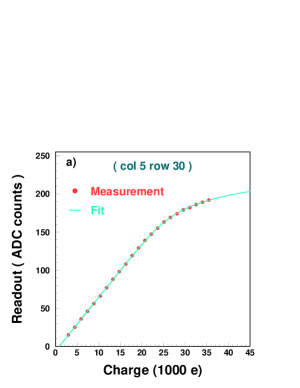
In Fig. 3, the pedestal subtracted and gain equalized spectrum of a Tb X-ray source measured for an FPIX0-instrumented detector is shown. The single channel calibration curve fits the data points very well. FPIX0 contains two different input cells characterized by different gains ( “high gain” and “standard gain”). In the following front-end characterization, the quoted central value gives the average quantity and the uncertainty gives the distribution rms within a chip. For most of the data taking, the discriminator threshold for the FPIX0 -stop was set to a voltage equivalent to 2500400 e- for the standard gain cells, and 1500230 e- for the high gain cells. For the FPIX0 -spray device the corresponding thresholds were typically 2200350 e- and 1250160 e-. The equivalent noise charge is 10515 e- for standard gain cells, and 8315 e- for for high gain cells of the FPIX0 -stop hybrid pixel devices. The corresponding values for the FPIX0 -spray devices are 8010 e- for standard gain cells, and 678 e- for high gain cells. An additional contribution due to the external buffer amplifier and ADC of about 400150 e- for FPIX0 standard gain cells and 20595 e- for FPIX0 high gain cells was present.
 |
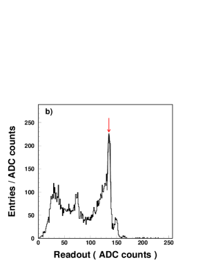 |
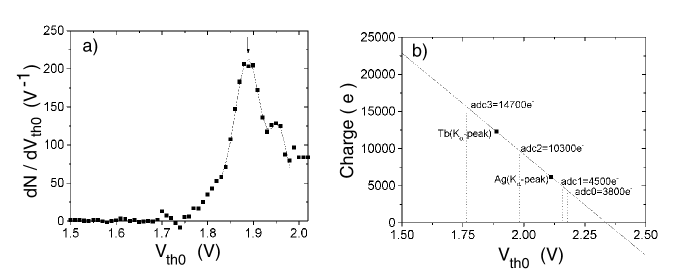
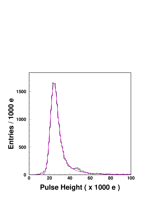
The absolute calibration of the FPIX1 readout chip response was determined by measuring the differential counting rate due to the same two X-ray sources. In Fig. 4 the differential counting rate obtained by sweeping the external voltage Vth0 for a hybrid detector exposed to a Tb source is shown. The peak of the derivative of the efficiency curve defines the threshold voltage Vth corresponding to the known Kα line. The procedure is repeated with a Ag source with a line producing a pulse height within the linearity range of FPIX1 to make an absolute measurement of the slope of the flash ADC response. The threshold used for FPIX1 -stop hybrid detector is 3,800 . In addition, the three thresholds determining the digitization bin sizes of the flash ADC were 4,500 e-, 10,300 e-, and 14,700 e-. The threshold dispersion for each discriminator was fitted to a Gaussian distribution. The standard deviation was in each case. The front-end equivalent noise charge is 11030 e-, where the quoted uncertainty reflects the rms spread within a chip.
4 Monte Carlo simulation of the pixel sensor performance
In order to identify the sensor and readout properties that are optimal for our experiment, we have developed a Monte Carlo simulation [4] including detail modeling of all the main physical processes affecting the development and collection of the signal in silicon.
Electrons and holes are produced by the energy deposited in the sensor by the charged track, and are simulated including excitations, low energy ionization [8], and energetic knock-on electron ( ray) emission [9]. The algorithm will be discussed referring to “” pixel sensors, where the relevant charge carriers are electrons. The drift motion of the electrons along the direction is described by the current density equation:
| (1) |
where is the magnitude of the electron charge, is the electron mobility and is the number of free electrons per unit volume. The speed is related to the electric field through the drift mobility . An experimental parameterization [10] is adopted, including non-linear effects at high fields.
The charge cloud spreads laterally due to diffusion. The parameter characterizing the drift in the electric field () is related to the parameter describing the diffusion of the charge cloud () by the Einstein equation:
| (2) |
where is the electron diffusion coefficient and is the product of the Boltzmann constant and the absolute temperature of the silicon. The average square deviation with respect to the trajectory of the collected charge without diffusion is . Note that in sensors, the region of highest electric field is the farthest from the signal electrodes. This is the region characterized by lower mobility and, consequently, lower diffusion coefficient. However the collection time is also influenced by the non-linear behavior of the drift velocity, thus the diffusion radius is less sensitive to this effect.
Fig. 5 shows the charge spread for track angles of 0 rad and 0.3 rad with respect to the normal to the detector plane. Diffusion determines the shape of the charge distribution at small incident angles and allows interpolation between pixel centers using charge weighting. At larger angles the charge division is linear and is dominated by the cluster broadening produced by the track inclination. The spatial resolution is determined by the precision of the charge measurement and by the pixel pitch. Our pixel detectors are expected to be very low-noise devices, as can be inferred by the data discussed previously. In order to take full advantage of this feature, the discriminator threshold spread needs to be small, as this spread needs to be added in quadrature to the intrinsic noise to determine the overall noise performance of the system. As mentioned before, the threshold spread measured in the devices used in the test beam was about 380 . Therefore noise and threshold spread figures are not limiting factors in the detector performance.

5 Data analysis and results
5.1 Analysis Method
The track position at each plane in the telescope is reconstructed using analog charge weighting. Each track is fitted to a straight line using the Kalman filter technique and tracks with a good are retained for further analysis. The Kalman fitter includes information from strip detectors and additional pixel sensors, but excludes the device under test. The track parameters allow the determination of the position () at which the beam intersects the sensor being characterized. Although the pixel detectors measure two coordinates, the discussion will focus on the resolution that can be achieved in the direction with smaller pitch, .
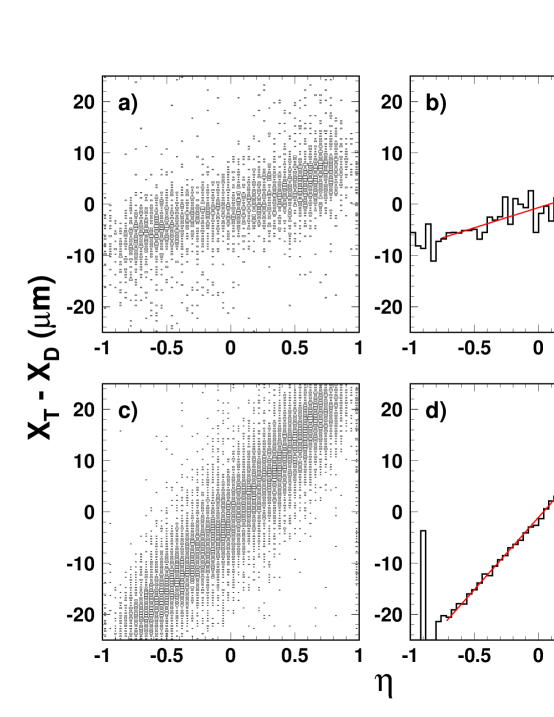
In order to predict the track impact point , it is important to align the individual detectors in the telescope. We use a right-handed coordinate system , where corresponds to the beam direction, is oriented along the vertical direction and is the horizontal axis. Each plane is defined by 3 offset parameters , and and three angles , and defining their orientation through three rotations around the , and axes respectively. We have developed two alignment procedures, implemented using the first 1000 events in a run. A “manual” technique finds the optimal values of some parameters, while maintaining geometrical parameters that are well measured at their known value. In a first iteration, translational offsets are determined such that the residual distributions are centered around zero. Next, the two relevant pixel plane angles, and are determined by minimizing the residual widths in the and directions. A second, automatic iterative alignment procedure has been developed performing a global minimization of the of the fitted tracks. This procedure guarantees that all the runs are aligned in a consistent fashion.
The coordinate measured in the pixel plane is determined in two steps. First we obtain the “digital” coordinate:
| (3) |
where xL (xR) is the local coordinate of the left-most (right-most) hit in the cluster. The “left” pixel is the one with the smallest coordinate.
Subsequently we refine this measurement with an empirical correction term expressed as a function of the variable [6] defined as:
| (4) |
where qR and qL are the charges deposited in the pixels located at the right and left boundaries of the clusters. Thus the measured position is given by . The correction is a function of the number of pixels in the cluster and the track angle, and is determined by fitting an independent data set.
The measured spatial resolution of a pixel plane is the difference between the reconstructed pixel position and the track position , known with an accuracy of about 2 m, limited by multiple Coulomb scattering from the material in the telescope and the intrinsic hit resolution of the various tracking stations. This prediction uncertainty is subtracted in quadrature from the measured spatial resolution in the results shown below.
5.2 Charge signal distributions
The 8 bit analog information provided by the FPIX0-based readout electronics allowed us to measure several features of the charge signal in various sensors. The measured pulse height distributions are fitted using a Landau function convoluted with a Gaussian [11]:
| (5) |
where N is a normalization constant, is the Landau probability distribution, with and is the most probable energy loss. For 300 of silicon we have 5.35 KeV, E 84.02 KeV, and 5.95 KeV. The study of the charge collected in single pixel clusters for tracks at normal incidence determines the straggling function in our sensor. This can be compared with model expectations and data from silicon strip sensors. The fit includes , , , as free parameters. Fig. 6 shows the pulse height distribution for an FPIX0 -stop sensor. The full width at half maximum (FWHM) is 10,000 .
The agreement with the parameters of the theory and with previous measurements in strip detectors [12] demonstrates that we are achieving full charge collection for -stop sensors. We can use the mapping of the average pulse height as a function of the track position to single out regions with poorer charge collection properties. Fig. 7 shows the average pulse height as a function of the track position for an FPIX0 -spray hybrid detector. There is an obvious dip at the boundary between two pixels in the direction, indicating a strong charge collection inefficiency. A less pronounced dip at the interpixel boundary in the direction is also present. This collection deficit is conjectured to be induced by a parasitic path to the bias grid, introduced to apply reverse bias to all the pixel cells during wafer testing of the devices [13]. An improved design of -spray sensors has been developed, and is expected to overcome this limitation [14].
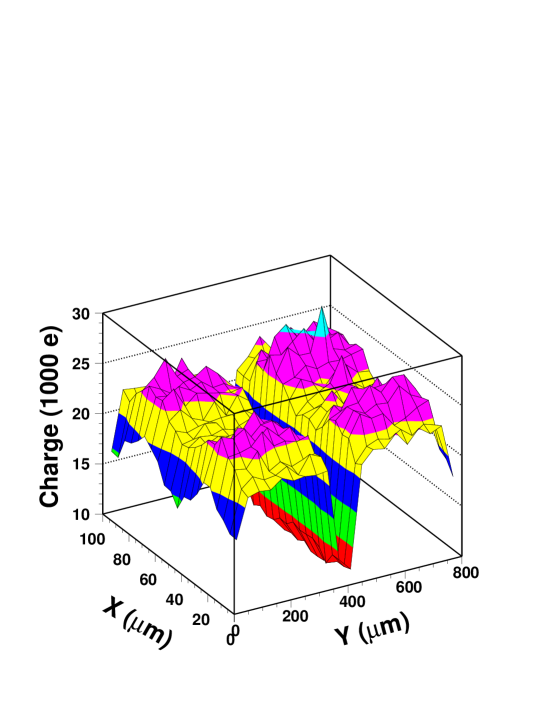
Table 1 summarizes the FWHM and the parameters of the Blunck-Leisegang function for various incident track angles.
| Angle[deg] | E/Ei | Emp/Ei | /Ei | FWHM/Ei | /Ei |
|---|---|---|---|---|---|
| 0 | 28900 | 2340028 | 146028 | 9600 | 279053 |
| 5 | 28400 | 2280044 | 152032 | 9610 | 271061 |
| 10 | 29600 | 2400043 | 150031 | 10400 | 325060 |
| 15 | 30200 | 2445045 | 161034 | 10670 | 293063 |
| 20 | 31800 | 2605047 | 165036 | 10680 | 330072 |
| 30 | 35000 | 3930064 | 166050 | 12800 | 400077 |
5.3 Pixel occupancy
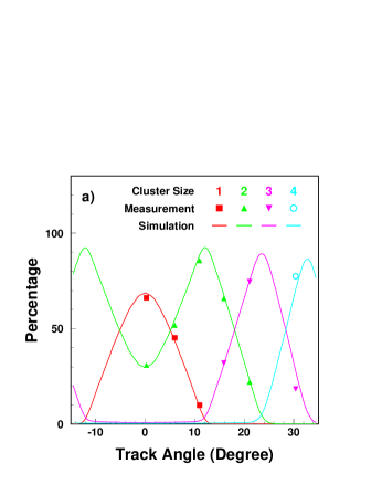
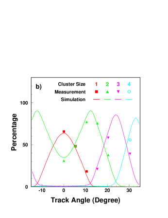
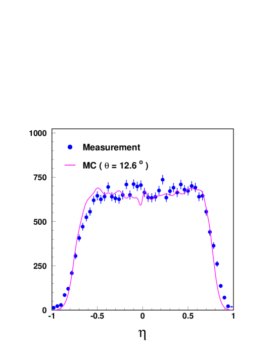
We performed a thorough study of the “row occupancy”, namely the number of pixels in a cluster as a function of the track incident angle and the sensor and electronics operating conditions. Fig. 8a shows the number of rows in a cluster as a function of the angle measured for FPIX0 sensors in nominal operating conditions as well as our Monte Carlo predictions. The agreement between data and simulation is excellent over the whole angular range studied. The FPIX1 based hybrid detectors have been studied with the same procedure, and the results are shown in Fig. 8b.
|
5.4 Position resolution
We studied the spatial resolution achieved with different sensor-readout electronics combinations for six track incident angles (0, 5, 10, 15, 20 and 30 degrees). The bias voltage was 140 V for CiS devices and 75 V for SII devices, corresponding to overdepleted sensors. The data sample was about 50,000 events per measurement. We also studied the sensitivity of our results to key parameters such as the bias voltage applied to the sensor and the discriminator threshold. We collected about 10000 events for each operation condition.
Only events containing a single reconstructed track, characterized by a cluster including at least two strips in the most upstream and downstream -measuring SSD planes are used in this analysis.
Fig. 9 shows the measured distribution for 10∘ tracks. An entry is made in these histograms only if adjacent pixels in a single column are hit. The curve shows Monte Carlo predictions for a track angle offset by 1.8∘ with respect to the value determined with the automatic alignment procedure described before. The 10∘ angle is chosen to determine the global offset reflecting a rotation of the beam axis with respect to our apparatus. This is because at this angle most of the tracks form 2 pixel clusters and thus the 2 pixel distribution has the best statistical power and can be predicted more accurately. The agreement between Monte Carlo and data is excellent, indicating that the various factors influencing the charge sharing are well modeled.
The empirical correction is determined by requiring that the average value of the residuals of the distribution is 0. The average residuals as a function of can be fitted with a variety of functions, the simplest one being a straight line. In the FPIX1 case, it is convenient to determine a correction for each of the 16 possible values of the pair . Fig. 10.a shows the difference between and the digital centroid as a function of for tracks at normal incidence; Fig. 10.b shows the linear fit to the residual average distribution ; Fig. 10.c and d show the corresponding plots for at 10∘ incident angle. We have determined a set of ’s using similar plots for each detector. This is done using independent track samples, dividing into 50 sub-intervals, and for each sub-interval determining the average value of .
The residual distributions for the FPIX0 -stop detector are shown in Fig. 11. Each distribution is fitted to a Gaussian. At small angles the residual distributions are non-Gaussian, because single pixel clusters are the dominant multiplicity and have a flat residual distribution. In addition there are non-gaussian “tails” due to the emission of -rays, that are discussed below. Nonetheless, the Gaussian standard deviations provide a commonly used measurement of the spatial resolution, that gives a reasonable parameterization of the dominant component of the residual distribution.
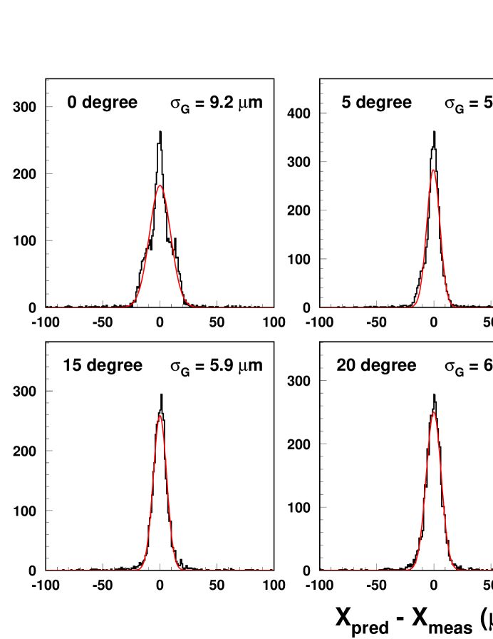
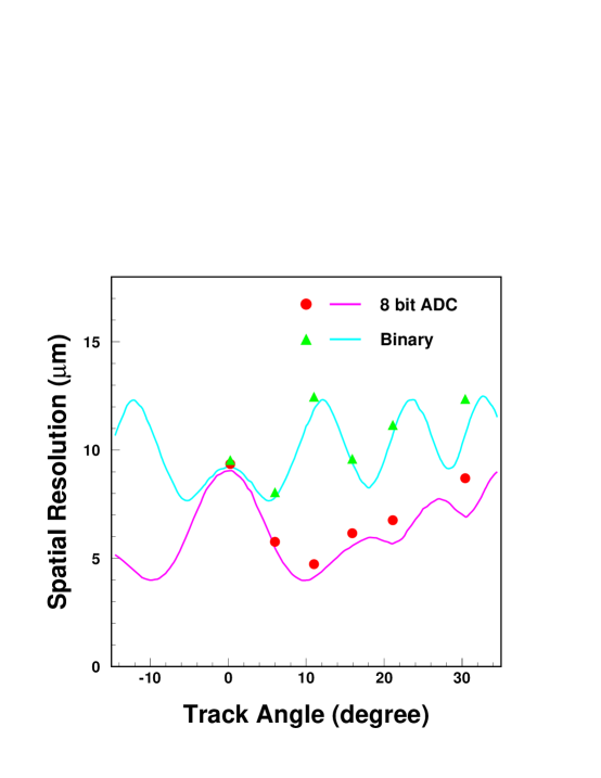
Fig. 12 shows the resolution as a function of angle. Two curves and data points are included: the solid line and circles show prediction and measurements done with an external 8 bit ADC; the dashed curve and triangular data points illustrate the results obtained using only , the binary reconstructed position, to simulate digital readout. Note the excellent agreement between simulation and data. The clear advantage of the analog readout is also evident. The binary interpolation is less accurate and features pronounced oscillations in the spatial resolution as a function of the track incident angle.
5.5 Resolution versus bias voltage and readout threshold
Data were taken with a variety of sensor bias voltages and readout thresholds. Fig. 13.a shows the predicted sensitivity of the spatial resolution on bias voltage for a -stop detector bump bonded to an FPIX0 chip with 8 bit analog readout. Fig. 13.b shows the corresponding data. A noticeable improvement in the resolution is obtained at small track angle when the reverse bias is close to the depletion voltage. This is because the longer collection time with lower bias voltage allows more charge sharing, thus reducing the percentage of the single pixel clusters.
 |
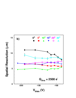 |
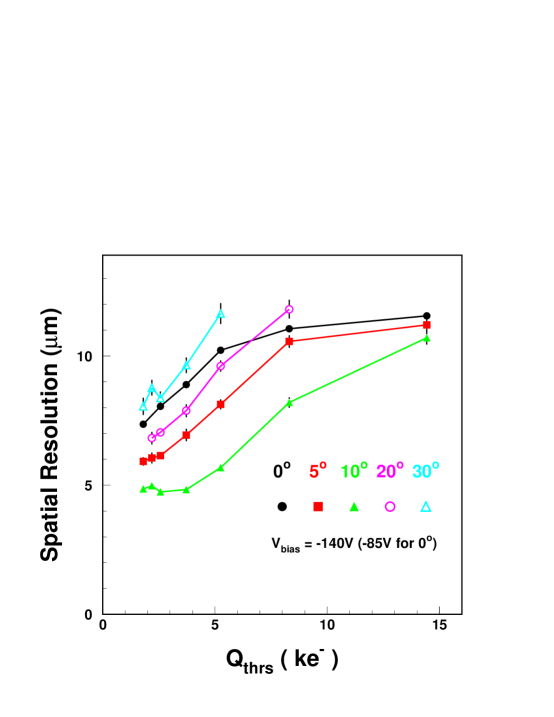
The discriminator threshold is one of the front-end electronics parameters that has considerable influence on the spatial resolution. Fig. 14 (top) shows the predicted effect of increasing the threshold for an incident angle of 300 mrad, for analog and digital readout. The bottom plot shows the fraction of events having pixels hit for a given threshold. For instance, for a threshold of 2000 electrons, about 50% of the events have 3 pixels hit, and about 50% have 2 pixels hit. As the digital clustering algorithm exploits the information provided by the number of pixels in a cluster, its accuracy is best when there is an almost equal population in two different cluster sizes: one cluster size corresponding to a track incident close to the pixel center and the other corresponding to incidence close to the boundary between two pixels. In the analog readout case, the accuracy of any position reconstruction algorithm is degraded as the threshold increases. Note that at increasing thresholds the efficiency becomes smaller, as illustrated by the curve N=0, corresponding to no pixel firing because all the charge signals are below threshold. Fig. 15 shows the corresponding measured data points for FPIX0 hybrid detectors.

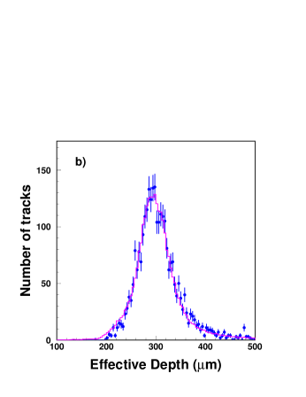
5.6 Effective depletion depth
The effective depletion depth of the detector can be measured from data at large track angle. We used two different methods. The first method has been originally proposed by ATLAS[16] to measure the effective depletion depth of irradiated and non-irradiated sensors. It consists of a track-pixel position correlation estimator, where for each pixel over threshold whose center is at position xi the distance zi between the track and the backplane is calculated with the formula: , where xinc is the x coordinate of the entrance point extrapolated by the fitted track and is the track incidence angle. The zi distribution is flat between approximate 0 and the effective depletion depth. The locations of rising and falling edges vary with different electronic thresholds. In order to estimate the depletion depth, a detailed MC simulation is needed.
The second method consists of a length-charge correlation estimator using the pixel charge within a cluster. For clusters including pixels, we can estimate an effective depletion depth , where qL,R is the charge collected by the pixel at the left (right) edge, qmiddle is the sum of the charge collected by the middle pixels, and is the pitch along . The distribution of the estimator zD is peaked around the effective depletion depth.
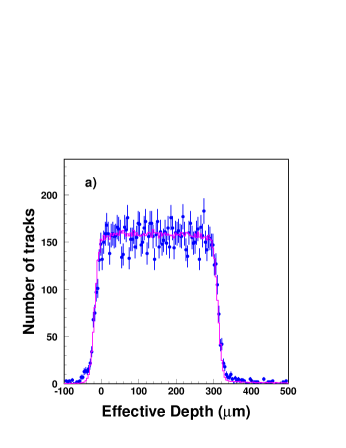
Fig. 16 shows the data and MC simulation for the CiS -stop-FPIX0 hybrid detector. Using , the effective depth is found to be m and m for the two methods respectively. The difference between two methods (m) can be used as an estimate of the uncertainties in the two methods. Note that this error corresponds to about 1∘ uncertainty in the track incident angle. So the depletion depth is m.
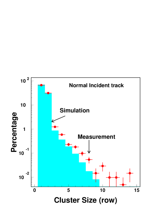
5.7 High multiplicity clusters
A small fraction of events have clusters with a number of hits greater than expected, given only the track trajectory and diffusion. Fig. 17 shows the measured frequency of high-multiplicity clusters for tracks at normal incidence. Our Monte Carlo simulation, which includes energetic -rays, reproduces the measured cluster multiplicity reasonably well.
5.8 Resolution function shape
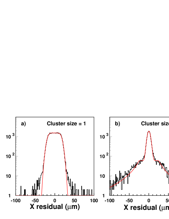
The pixel residual distribution (or resolution function) deviates from a Gaussian in two ways: the first effect is produced by the non-optimal the charge sharing at almost normal incidence that produces a large fraction of 1 pixel clusters; the second is related to large cluster size events due to delta-ray emission. These effects have been alluded to before and are now discussed quantitatively using a sample of tracks at nominal normal incidence.
Fig. 18 shows the residual distributions for the FPIX0 -spray detector taken with the beam nominally at normal incidence. The plot on the left shows the residual for one-pixel clusters. The plot on the right shows the residual for clusters of two or more pixels, with a fit with the function :
| (6) |
where is a Gaussian, and is defined as:
| (7) |
is a normalization constant, is the half width of the constant term, and is the exponent of the power-law dependence. The non-Gaussian fraction accounts for 18% of the total number of entries in the distribution.
The naive expectation of a rectangular shape 50 m for the residual distribution for one pixel clusters is distorted by two effects. The population at the “edges” of the rectangle is depleted by diffusion, inducing two pixel clusters for track incident near the pixel periphery. On the other hand, a broadening of this ideal distribution is induced by threshold dispersion and electronic noise, as well as the small fraction of mismeasured extrapolated position .
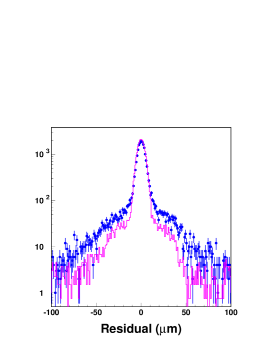
The second factor that makes the pixel residual distributions non-Gaussian is -ray emission. Low energy -rays which stop in one of the pixels crossed by the particle skew the charge sharing and degrade the resolution. Higher energy -rays cross one or more pixel boundaries and distort the position measurement even more. We have studied this effect with the Monte Carlo simulation described before. Fig. 19 shows a comparison between predictions and data. The distributions are shown using a log scale to show the tails of the residual distribution more clearly. The simulation accounts for about 1/2 of the broad component of the residual distribution. This may be in part due to instrumental effects such as the charge losses near the pixel boundaries of the -spray devices.
5.9 Charge sharing across columns
Charge-sharing between columns occurs for less than of the tracks in our data sample. We collected enough data to study this effect only at 0∘, where the diffusion is the basic sharing mechanism.
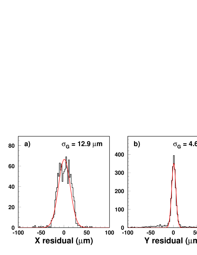
For -stop sensors the effective charge sharing region is a rectangular ring with approximately uniform thickness along the pixel boundary. Fig. 20 shows the residual distributions and of 1 row and 2 column clusters. The measured is calculated with the procedure described before, using a linear eta correction determined from the data. The spatial resolution along is consistent with the resolution when charge sharing allows for interpolation between the pixel centers.
6 Conclusions
An extensive test beam study of several hybrid pixel detectors has demonstrated that both the sensors and the front-end electronics chosen for BTeV perform according to expectations. The charge collection properties of the sensors studied are well understood. We have shown that 2-bit analog information is satisfactory and, consequently, that the final version of the front-end electronics, featuring a 3-bit flash ADC will provide the excellent spatial resolution needed to achieve the BTeV physics goals.
7 Acknowledgements
We would like to thank Fermilab for providing us with the dedicated beam time for our test and the excellent infrastructure support. We are grateful to the ATLAS collaboration, with special thanks to their pixel group for the sensors that were used in this test and many useful discussions. We are indebted to Colin Gay for the data acquisition software. We also thank the US National Science Foundation and the Department of Energy for support. The Universities Research Association operates Fermilab for the Department of Energy.
References
- [1] A. Kulyavtsev, et al. BTeV proposal, Fermilab, May 2000.
- [2] E. E. Gottschalk, Fermilab-CONF-01-088-E, June 2001.
- [3] T. Rohe, et al., Nucl. Instr. and Meth. A409 (1998) 224.
- [4] M. Artuso and J. C. Wang, Nucl. Instr. and Meth. A465 (2000) 115; J. C. Wang et al., hep-ex/0011075 (2000).
- [5] D.C. Christian, et al., Nucl. Instr. and Meth. A 435 (1999) 144.
- [6] R. Turchetta, Nucl. Instr. and Meth. A 335 (1993) 44.
- [7] P. Billoir, Nucl. Instr. and Meth. 225 (1984) 352-366.
- [8] GEANT, CERN Program Library Long Writeup W5013 (1994).
- [9] M. Pindo, Nucl. Instr. Meth A 395 (1997) 360.
- [10] K. Kaufmann, B. Henrich, CMS Internal Note 2005/000 (2000).
- [11] O. Blunck and S. Leisegang, Z. Phys. 128 (1950) 500.
- [12] S. Hancock, et al., Nucl. Instr. and Meth. B1:16 (1984) 16.
- [13] M. S. Alam, et al., Cern-EP/99-152
- [14] Nucl. Instr. and Meth. A 460 (2001) 55.
- [15] E. Belau et al., Nucl. Instr. and Meth. 214 (1983) 253.
- [16] I. Gorelov et al., CERN-EP/2001-032, (2001).
- [17] T. Zimmerman, et al., IEEE Trans. Nucl. Sci. Vol. 40 No.4 (1993) 736.
- [18] S. Zimmerman, et al., IEEE Trans. Nucl. Sci. Vol. 43 No.3 (1996) 1170.
- [19] C. Jacoboni, et al., Solid-State Electronics 20 (1977) 77-89.
- [20] G. Hall, Nucl. Instr. and Meth. 220 (1984) 356.
- [21] A. Mekkaoui, Nucl. Instr. and Meth. A465 (2000) 166.
- [22] R. Turchetta, Nucl. Instr. and Meth. A 335 (1993) 44.