Compact Frontend–Electronics and Bidirectional 3.3 Gbps Optical Datalink for Fast Proportional Chamber Readout
Abstract
The 9600 channels of the multi–wire proportional chamber of the H1 experiment at HERA have to be read out within and made available to the trigger system. The tight spatial conditions at the rear end flange require a compact bidirectional readout electronics with minimal power consumption and dead material.
A solution using 40 identical optical link modules, each transferring the trigger information with a physical rate of via optical fibers, has been developed and commisioned. The analog pulses from the chamber can be monitored and the synchronization to the global HERA clock signal is ensured.
1 Introduction
An optical link and frontend electronics has been developed to read out all 9600 channels of the H1 experiment’s central inner multi–wire proportional chamber (CIP) within the time between two bunch crossings, i.e. . The application requires a bidirectional multi–purpose link: the digitized chamber information has to be provided to the trigger system away, selected analog pulses should be accessible for monitoring purposes and the whole frontend electronics must be synchronized to the global HERA clock signal. Furthermore, the optical link and readout electronics must fit in the available space of a long open cylinder with inner and outer radii of and . No commercial solution for optical links fulfill these requirements in one compact unit.
The custom–made solution is composed of forty identical optical link modules, where a 64–fold multiplexing reduces the number of data lines. Each module performs an optical transmission with a physical rate of . Precisely aligned VCSEL and PIN diode arrays allow for bidirectionality. The bending of optical fibers by within minimizes the overall height of the design.
A short overview of the CIP upgrade is given in Section 2 and the general layout is discussed: Each of the optical link modules consists of an on–detector unit, two optical hybrids with optical cables and a receiver unit. Their functional designs are presented in Sections 3, 4 and 5, respectively. The performance of the optical link and frontend electronics is presented in Section 6.
2 CIP Upgrade and General Layout
With the year 2000 upgrade of the HERA electron–proton collider at DESY, an increase in luminosity by a factor of five is anticipated. The expected higher background rate, predominantly beam–wall and beam–gas reactions, necessitates an improvement of the CIP to provide high background rejection efficiency of the –vertex trigger [1, 2].
The redesigned CIP [3] is built of five concentrical cylinders (layers) with radii from to . In the azimuthal angle, each layer is equally subdivided into 16 segments, each consisting of 120 pads111In fact, the CIP uses a projective geometry requiring 119 pads on the innermost layer, and 112, 106, 99 and 93 pads on the following layers, respectively. But for symmetry reasons, each optical link module will be capable of handling 120 pads. along the symmetry axis (–axis). Charged particles traversing the chamber are detected by the 9600 pads, which provide space points and timing information. The direction of tracks can be inferred from the pattern of hit pads. For electron–proton collisions intersections of tracks with the –axis come mostly from the interaction region, while the dominating background originates from proton beam losses upstream of the experiment. Experience has shown, that such background tracks seen by the H1 experiment are typically intersecting the –axis at to upstream of the mean interaction position. A new trigger system based on the latest FPGA family will identify these upstream events and is presently being commissioned. According to simulations this new trigger will improve the background rejection capability of the first level trigger by an order of magnitude compare to the previous –vertex trigger [4].
The decision has to be made for every bunch crossing. Thus all 9600 pads have to be read out within the time between two bunch crossings, i.e. within , corresponding to the bunch crossing frequency of (HERA clock). From the timing information, the bunch crossing number can be deduced.
Each of the forty identical optical link modules is used to read out all pads of two adjacent segments (a double–segment) of a layer with a rate of . The on–detector electronics unit amplifies and shapes the signals from the pads, discriminates and serializes them to words. After a second level 16–fold multiplexing, this trigger information is transferred to the receiver electronics unit away, located outside the main detector. Thus the total digitized information per module sums up to a data rate222In principle, each optical link module is capable to transmit at a data rate of at maximum. of . The on–detector electronics component must be synchronized to the global HERA clock signal therefore the system requires bidirectionality. The receiver electronics provides the global HERA clock and retrieves the multiplexed trigger information, which is de–serialized and distributed to the trigger system. Additionally, analog signals from each pad are transmitted and accessible for monitoring purposes.
To retain high geometrical acceptances for the new CIP and neighbouring detectors in the H1 experiment, the available space for mechanical support structures and electronics is limited to a long open cylinder with inner and outer radii of and , respectively, located at the backward end flange333The term “backward” labels the end of the H1 experiment pointing in the direction of the electron beam. of the CIP.
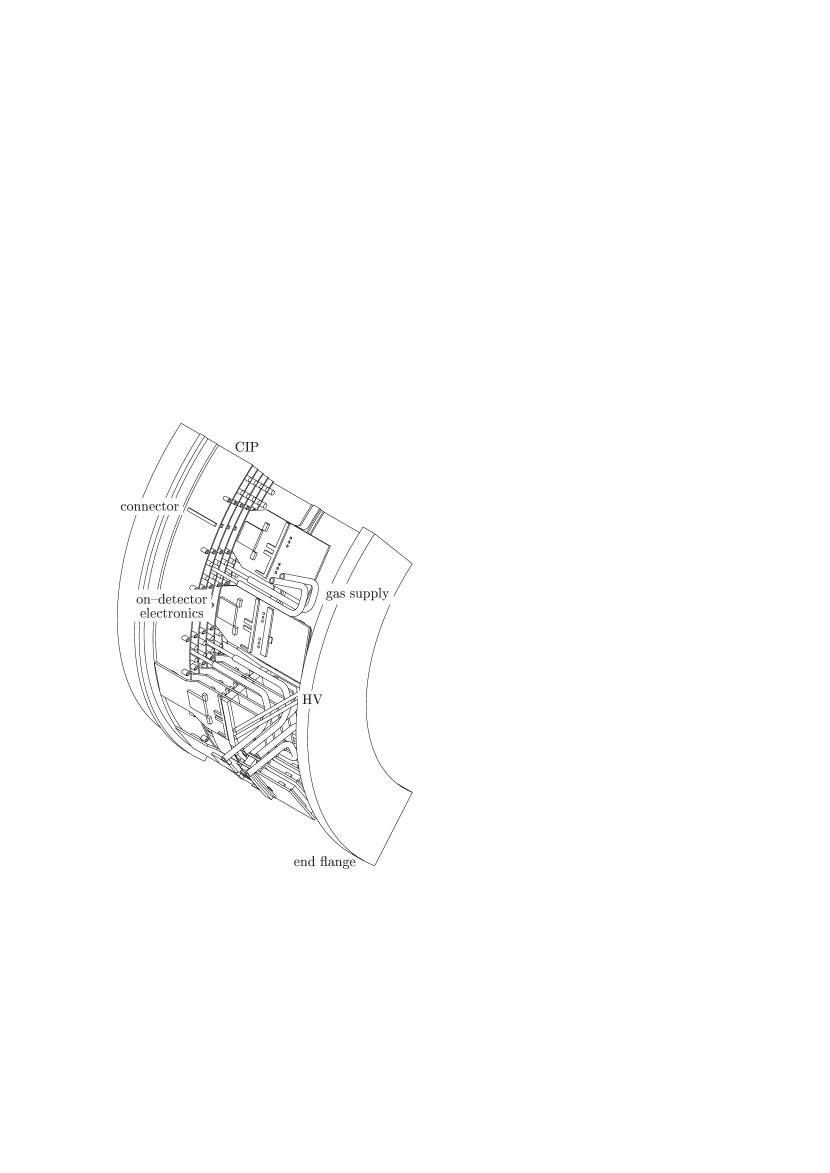
This tight space has to be shared between on–detector electronics, their suspension and cooling, low and high voltage power cables and gas supply lines (Figure 1). The power consumption has to be minimized to avoid an excessive heat dissipation inside the H1 experiment due to limited cooling possibilities.
Only an optical transmission allows high serial data rates, suppresses crosstalk and decouples detector and trigger system, while reducing the number of cables and the power consumption to a minimum. A readout with copper cables as formerly done would increase that volume by a factor of ten, would require even more driving power and would produce an unwanted high contribution to the dead material. In addition, an electrical transmission at the required high rates will likely induce noise into the very sensitive liquid argon calorimeter of the H1 experiment.
The optical link between on–detector electronics and the receiver electronics is established by two optical hybrids which perform opto–electrical (re)conversion of all data lines, i.e. four digital channels for the trigger information, two analog channels and two channels for the HERA clock signal. Experience with opto–mechanics has already been collected in the ETH Zurich group. An analog optical readout for the H1 experiment has been successfully operated since 1995 [5, 6].
3 On–Detector Electronics Unit
Each on–detector unit collects the charge from pads. Their charge is conducted via micro coax cables [7] to the rear end flange of the CIP. For each segment, a connector (Fujitsu FCN 298 [8], 120 contacts, pitch, height) passes the 120 channel pad information to a pair of analog readout (CIPix) chips. The CIPix chip amplifies, shapes, discriminates and four–fold multiplexes the signals. Further compression is done by two 16–fold multiplexers, each driving a differential high–speed data channel at . After electro–optical conversion by the optical hybrid, the light pulses are transmitted to the receiver electronics unit. The overall synchronization is done with the global HERA clock signal received by the optical hybrid. A low jitter phase–locked–loop (PLL) unit [9] generates a clock signal, which is distributed to the multiplexer and — in addition to the HERA clock signal — to the CIPix chip. Furthermore, selected analog signals can be branched off before entering the CIPix discriminator to monitor the CIP. These analog test signals are also transmitted (Figure 2).
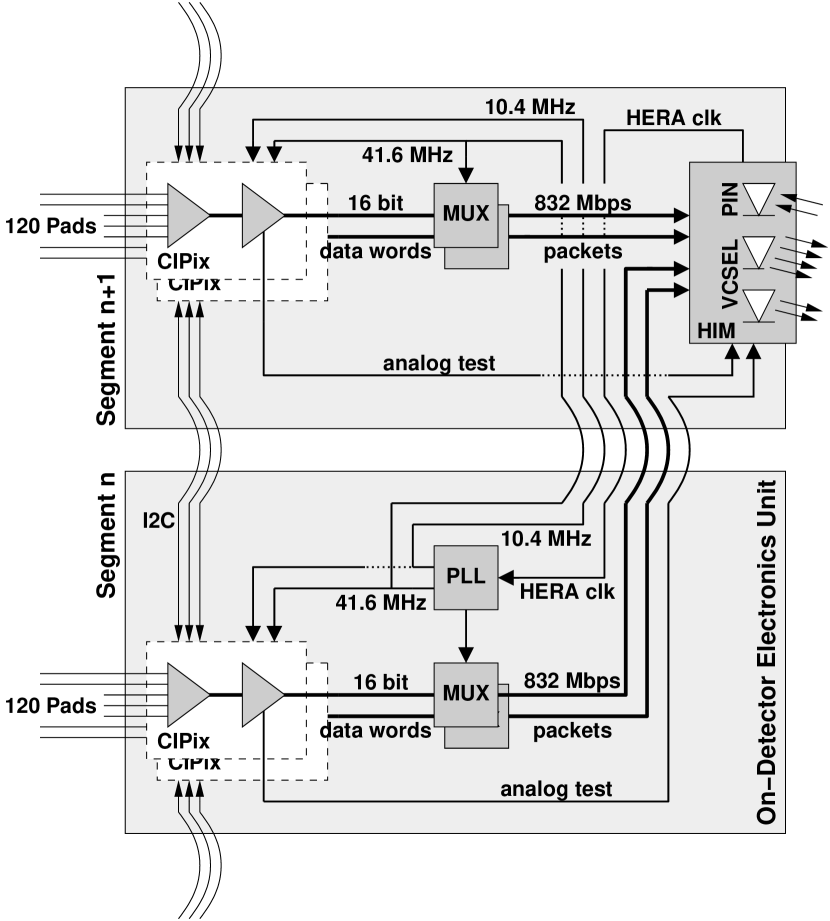
For compactness, one optical hybrid serves a double–segment and is mounted on one of the two separate halves of the on–detector unit. The other half holds the PLL unit and houses the voltage regulators. Due to the curvature of the CIP, a thin four layer flex–capton print bridges all signals via striplines to their destinations: The high–speed data channels and analog test signals are transferred from the other segment to the optical hybrid and, in return, the HERA clock signal is provided to the PLL unit. The flex–capton print is sandwiched between each of the halves. This rigid–flex print is produced by Dunkel & Schürholz [10]. It is implemented as an extremely high dense board with microstrip transmission lines and eight layers in total (Figure 3).
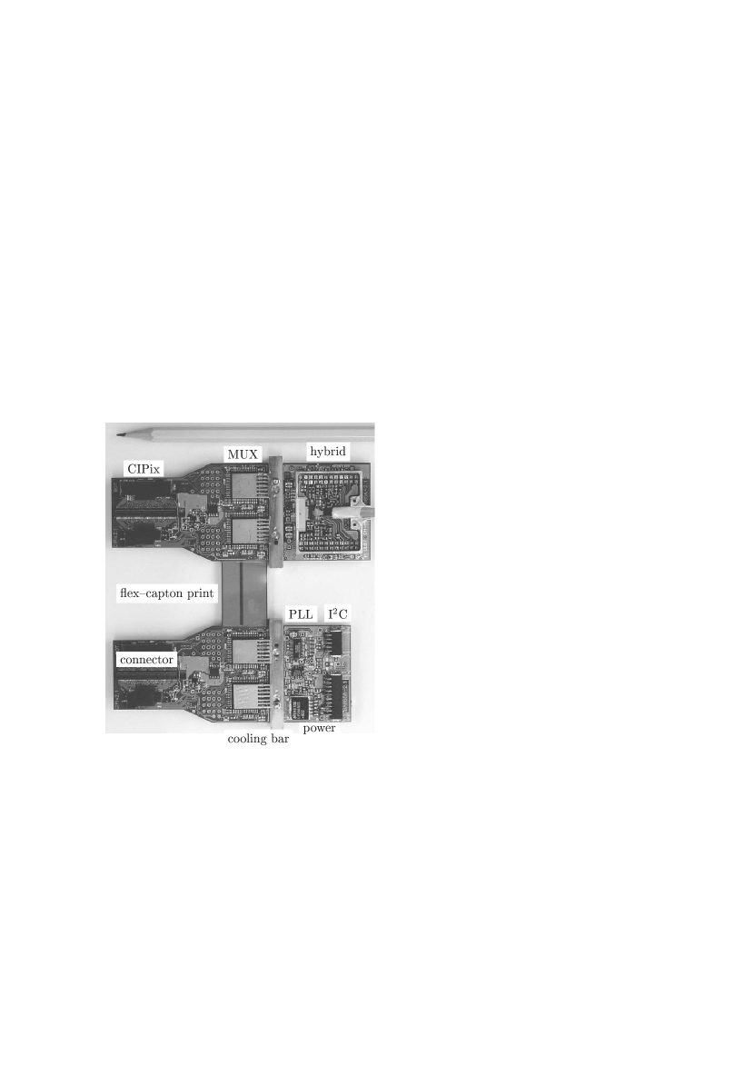
Its outer dimensions are in length, in width and in height. The open length of the capton print, i.e. the distance between both halves, increases proportional to the layer radii.
All on–detector units of one layer are connected via an I2C bus daisy–chain [11]. This allows for a steering of every CIPix chip from a terminal, e.g. all CIPix chips can be initialized layer–wise. In addition, it performs a one–wire serialized temperature measurement [12].
3.1 CIPix IC
The CIPix analog readout chip is custom–made [13]. It amplifies, shapes, discriminates and multiplexes the incoming signals [14].
For each of the 64 analog input channels, it consists of a charge sensitive preamplifier with a gain of per electrons, a CR–RC semi Gaussian shaper with a peak time of to and a comparator. The discriminated signals are synchronized to the HERA clock signal and four adjacent pads are multiplexed (Figure 4).
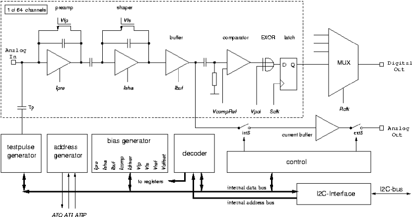
For monitoring and testing purposes, one of the analog signals can be selected and branched off to an analog output. Test pulses of user–defined pattern and frequency can be internally generated. Comparator thresholds, the selection of channels for analog output and test pulses are programmable via the I2C bus. To protect the bond–wires and the surface, each CIPix chip is sealed (“glob–topped”) with protective glue (Epoxy Technology H70S [15]).
The analog signals from 60 pads are processed by a single CIPix chip. Synchronously to the clock signal, the CIPix’s 15 digital output channels give four successive words with each. A FirstWord bit tags the first of these words and will make it possible to maintain the synchronization to the HERA clock signal in the trigger system. Together they form the data word. An EmptyDataSet signal, generated in the case of missing inputs on all 60 input pads of the CIPix chip, serves as the EmptyDataSet bit. All 160 EmptyDataSet bits provide a coarse readout and will be used for a trigger decision whether an event is compatible with cosmic ray background or not.
3.2 Multiplexing / Demultiplexing
A further reduction of channels is achieved by building a differential high–speed data link for point–to–point communication between the Hewlett–Packard HDMP 1032 transmitter and the HDMP 1034 receiver [16].
Both bipolar chips provide the transmission of a TTL data word plus one flag bit with a serial data rate of to . The rate is chosen by an external reference clock signal synchronous with the incoming word. The HDMP 1032 PLL / clock generator locks onto the reference clock signal and multiplies it up to the high–speed serial clock signal. From the data word a special four bit encoding information is generated on the fly, proceeding the data word. Together they give a packet. On the one hand, the encoding ensures the DC balance of the serial line. The disparity444The disparity is defined as the total number of “high” bits minus the total number of “low” bits. of each data word is determined. Depending on the disparity of the previous data word, an inversion of the actual word is done to keep a duty cycle. Additionally, the encoding bits provide an error detection, tagging wrongly transmitted words, and include an user–controlled flag bit. On the other hand, the unique bit pattern of the encoding scheme incorporates the high–speed clock signal and thus saves an additional clock signal line between transmitter and receiver. The packet is serialized and leaves the HDMP 1032 as a differential terminated ECL compatible high–speed signal.
The HDMP 1034 receiver’s Clock Data Recovery unit separates encoding bits and data word from the packet, extracts the high–speed serial clock signal and locks to its phase. The data words are (eventually) inverted and then demultiplexed. The Parallel Automatic Synchronization System synchronizes these words to an external reference clock signal. A master–slave mode allows for a synchronization of several HDMP 1034 chips: A deviation of the relative phase of the data word and the reference clock signal generates a shift request, passed to the master. The master controls the delay of all outputs of all slaves.
Each data word is serialized by a HDMP 1032 chip. The EmptyDataSet bit is used as input for the flag bit; the clock signal provides the reference clock signal for both HDMP chips. Therefore the digitized trigger information from 60 pads is transmitted every with a data rate of . The overall physical rate includes in addition per the four FirstWord bits and bits of the encoding scheme (with the EmptyDataSet bit) and amounts to . The receiver chip re–parallelizes the trigger information and extracts the FirstWord bit and EmptyDataSet bit. Four transmitter / receiver chip pairs — one for each CIPix chip — are used per module.
Bits of one high–speed digital channel have been superimposed for the eye–diagram (Figure 5).
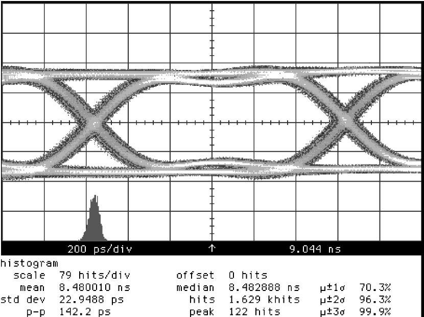
The rising and falling edges are well separated. The measurement of the zero–crossing of the rising edge results in a jitter of the data words of before entering the optical hybrid.
4 Optical Hybrid
The optical hybrids constitute the interface between the electrical and the optical régime.
Following the signal flow from the CIP to the trigger system, the optical hybrid on the on–detector unit (HIM, High–Speed Interconnection Module) acts as a driver for the outgoing packets and analog test signals and as a receiver for the incoming HERA clock signal. The optical hybrid on the receiver unit side (DeHIM) acts vice versa. The interfacing pins require or deliver differential CMOS logic signals for each data channel, respectively.
Each HIM / DeHIM pair serves one double–segment, i.e. transmits four multiplexed data channels with a physical rate of , two analog test signal channels and two HERA clock signal channels via an optical fiber array with eight fibers.
The four data channels are driven by the Helix HXT 2000 [17] chip optimized for vertical cavity surface emitting laser (VCSEL) diodes. The VCSEL diodes convert the electrical signal to light pulses. After of optical fibers, conventional PIN diodes reconvert the optical to electrical signals. These are amplified by the Helix HXR 2004 receiver chip and produce four differential data signals. Because of the high data rates, the hybrid boards are impedance controlled and realized in four–layers with layer–to–layer blind–via connections [10].
For redundancy two HERA clock signals are transmitted in parallel. Standard SZ 125 drivers match their signal levels with respect to the VCSEL diode specifications. Conexant (formerly Microcosm) MC 2007 receivers [18] convert the PIN diode responses back to voltage–modulated signals. Its active gain control (AGC) ensures a stable output signal above the sensitivity limit at about . The two analog test signals are driven by Maxim MAX 4212 operation amplifiers [19] and received by Conexant MC 2011 (without AGC) chips. These differential analog signals and the HERA clock signal are finally amplified by Maxim MAX 4212 chips.
4.1 Driver and Receiver Circuits
The Helix HXT 2000 driver and the HXR 2004 receiver chips are designed for high–speed optical transmission up to per channel; the HXT 2000 is optimized for VCSEL diodes at to wavelength. The differential inputs to the HXT 2000 — four of them enabled — are amplified and current–modulated. External resistors allow to control the average and modulation current collectively for a VCSEL diode array. Thus the working range, i.e. the laser current, of an array of four VCSEL diodes can be optimized for maximum optical output.
The four channel HXR 2004, compatible to photodiode arrays, converts the photocurrent from the PIN diodes to differential output voltages. In addition, the average photocurrents can be monitored.
4.2 Vertical Cavity Surface Emitting Laser Diodes
Laser diodes convert current–modulated signals into power–modulated light signals.
In a VCSEL diode the light propagates vertically through the structure (Figure 6).
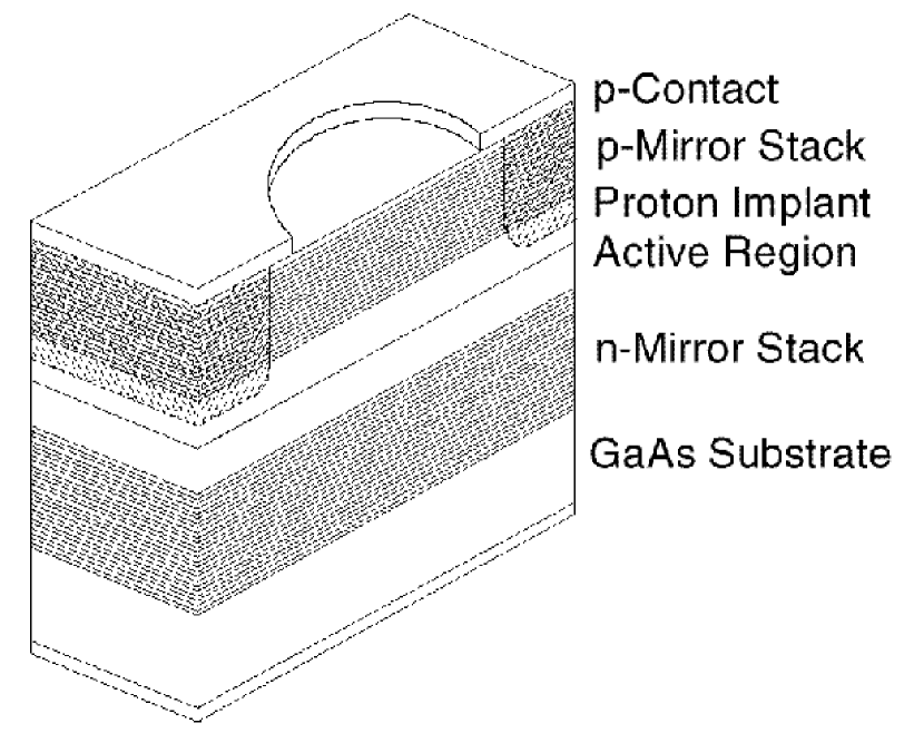
With this orientation the laser cavity can be grown to match the wavelength of the laser light, i.e. . The total spectral width of the emission is generally less than , which ensures a low coherence source. The beam divergence is typically below FWHM. Alternating layers of AlAs and Al0.15Ga0.85As provide the p– and. n–mirror stack surrounding the active region, respectively. With contact to the p–mirror, the VCSEL anode is bonded to the modulating current line, while the GaAs substrate holds the cathode i.e. ground potential [20]. Both, VCSEL and PIN diodes, are grouped in six– and two–diodes dies, respectively, from Truelight Corporation [21]. The specifications for the VCSEL and PIN diode arrays used are given in Table 1.
| Optical specifications: | VCSEL | PIN |
|---|---|---|
| Wavelength | 850 nm, multimode | |
| Beam profile and divergence | round, | |
| Active / Sense area diameter | ||
| Slope efficiency / Response at | ||
| Electrical specifications: | VCSEL | PIN |
| Serial impedance | typ. | |
| / | ||
| @ | ||
| Crosstalk | ||
| Mechanical specifications: | VCSEL / PIN | |
| Operating temperature | ||
| Chip thickness | ||
| Pitch diode / diode | ||
The VCSEL diodes are specified as “class IIIb laser” in the safety standard ANSI Z136.1 [22] and have to be treated as a potential eye hazard.
Because of a delicate passivation, the softer ball–bond process using golden bond wires has been preferred to the wedge–wedge bonding and to the use of aluminum bond wires. Thus ultrasonic vibrations acting on the VCSEL diodes could be minimized and harm to the passivation could be prevented. Together with the required specifications of at least at laser current (i.e. to a slope efficiency of ) and an uniform power gain over the VCSEL array, the yield has been tested to be about .
The lasering of the used VCSEL diodes typically starts at a current of (Figure 7).
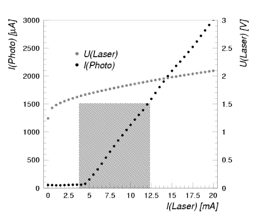
With appropriate settings for the average and modulation current of the HXT 2000 ( and , respectively) the working range has been optimized. The digital signal levels vary beween for logical “low” and for logical “high”, leading to a dynamic range in optical output of approximately . The uniformity over a VCSEL diode array is about .
4.3 Alignment and Bending
In case of the HIM, the sixfold VCSEL and twofold PIN diode arrays are aligned with a precision of with respect to each other and with respect to two guiding pins [23]. This provides a pitch of in order to match the pitch of conventional fiber ribbon connectors (MTP connectors [24]). The guiding pins adjust the connector to the diode arrays (Figure 8).
To obtain the desired precision, each diode array is positioned by a custom–made micro manipulator. The manipulator is mounted on an table, which makes it possible to perform an accurate position measurement and an optical survey. At its final position, the diode array is lowered and glued onto the hybrid. An optimal mechanical and optical performance has been achieved using a two component conductive glue (Epoxy Technology H21D [15]) with a resistivity of and a bakeout time of . On the DeHIM side, sixfold PIN and twofold VCSEL diode dies are aligned with the same accuracy.
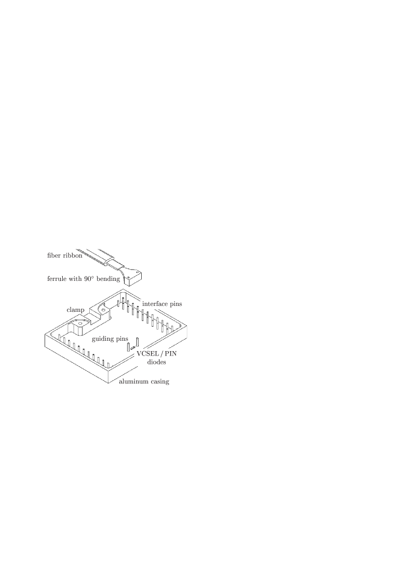
Since the distance between two CIP layers is less than , it is not feasible to mount the MTP connector above the VCSEL / PIN array. Even if the connector is reduced to its inner core, namely the ferrule, adjusting the ferrule perpendicular to the hybrid leaves no space to properly fix the connector to the optical hybrid. In addition, it complicates the installation of the fibers at the end flange. Consequently the ferrule had to be mounted parallel to the optical hybrid, i.e. parallel to the –axis. Since the diodes send the light perpendicular to the die, the light needs to be redirected. Therefore the fibers are bent within of height by modifying the ferrule and by using special fibers (GGP fibers from [25]). The performance of the transmission line has been measured to remain stable while the attenuation at each deflection lies below . On the DeHIM side, the fibers are conventionally bent within .
Each optical hybrid is embedded in an aluminum casing to provide robustness and handiness, to avoid electrical induction from outside and to shield the VCSEL and PIN diodes from dust. Its outer dimensions are . Clamps at the aluminum casing give a proper mechanical connection of the hybrid with the fiber tails of length ( at the DeHIM) and prevents outside stress to affect the precise mechanical adjustment of the ferrules to the diodes.
4.4 Optical Cables
In guiding the optical fibers out of the main detector, several aspects have to be taken into account. Safety rules demand that all fibers and the sheathings be halogen–free and inflammable, space constraints require low bending radii of the cables, the CIP and parts of the on–detector electronics should be as easy to maintain as possible and all cables need to have a connection at the cable distribution area (CDA) at the backward end of the CIP. For these reasons, the optical transmission line is divided into four parts. Starting at the HIM, its fiber tail is plugged to a long fiber ribbon cable ending at the CDA. From there, a cable feeds the signals to the electronics cabin outside the main detector and is connected to the tail firmly attached to the DeHIM casing.
The tails, including the bending part, are produced by Schütten Optocommunication [26]. The long distance cables and tails are made by Infineon [27]; the short distance cables are from Siecor [28]. The specifications of the cables are listed in Table 2.
| Mechanical specifications: | |
|---|---|
| Fiber count / type | |
| Flame resistance | UL-910 (Siecor) |
| LSZH (Infineon) | |
| Dimensions | |
| Minimum bending | |
| radius (long term) | |
| Optical specifications: | |
| Maximum attenuation | |
| Minimum bandwidth | |
| Numerical aperture | |
All cables are assembled with standard MTP connectors (except the ferrule end of the tails) with a typical attenuation of to at each MTP–MTP connection and three connectors per link. Adapters from AMP [29] attach two MTP connectors to another. To obtain a predictable timing between different modules, all cables of each type are chosen to have equal length. Measurements give an average length of and , respectively.
5 Receiver Electronics Unit
The receiver unit provides the signals of four adjacent pads, i.e. four successive data words and the EmptyDataSet bits, to the trigger system (Figure 9).
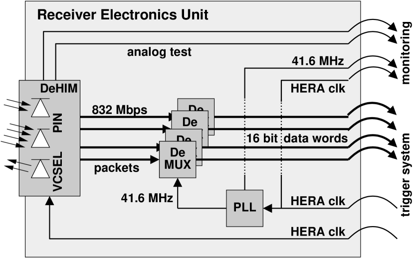
The DeHIM receives the high speed data signals and passes them to the four HDMP 1034 demultiplexers regaining the data words. The demultiplexers are used in the master–slave daisy–chain mode to maintain synchronization of all words, at which anyone of the HDMP 1034 can serve as master. Latches feed the four–fold multiplexed data words and the EmptyDataSet bit with a rate of to the backplane that connects the trigger system and the receiver electronics. The incoming global HERA clock signal is received from the backplane and directed via the DeHIM to the on–detector PLL unit. It is also passed to the receiver board’s low jitter PLL unit [9] producing the HDMP 1034 reference clock signal. This clock signal and the FirstWord bit are used in the trigger system for the synchronization of different receiver units.
The receiver unit board is implemented as a six layer, high density and high speed board with microstrip transmission lines produced by Alwaprint [30]. At the receiver unit’s frontplate, the following signals are available for monitoring purposes: the data word, the EmptyDataSet bit, the differential analog test signals, the HERA– and the clock signal.
6 Performance
The optical link modules will be operated inside the H1 experiment in a magnetic field and only to away from the electron beam. Thus they will be exposed to synchrotron radiation and not be accessible from outside without major effort.
Therefore, the modules needed to be tested beforehand for long–term stability, reliability and robustness. Special attention has been paid to the bit–error rate, the transmission of the analog signals and the power dissipation.
Prototypes of the modules have been successfully operated since November 1999. Neither a break–down of any of the used components nor a decrease in the power output of the VCSEL diodes have been observed.
6.1 Link Performance
As soon as the global HERA clock signal is applied, each link module runs autonomously. The PLL unit of the on–detector electronics locks on the HERA clock signal and distributes the HERA– and clock signals to the CIPix chip and multiplexer. After the multiplexer has been able to lock on the clock signal and the optical link is established. Frequency changes of the HERA clock signal within a window of to have been proven to be tolerable.
For random data words, i.e. words with duty cycle, the average light yield has been measured to be at the DeHIM’s end of the link after and three connector pairs. The PIN diodes’ high response of typically drives the HXR 2004 receiver into saturation, thus noise is suppressed. From the measurement of the bit–error–rate (see below), the lower limit has been estimated to be approximately . An eye–diagram of the digital information directly at the demultiplexer’s input is shown in Figure 10.
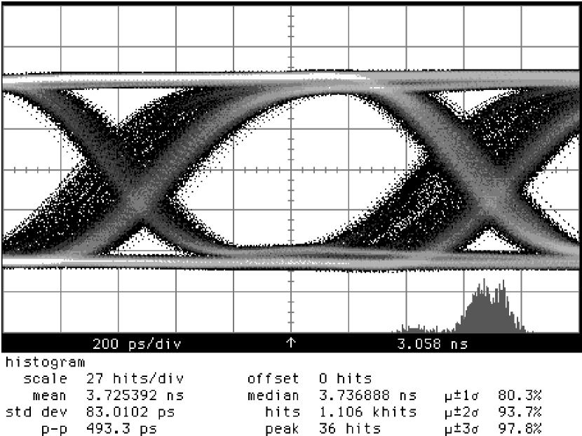
The rising and falling edges are well separated. The jitter of the packets is about . A few percent of the entries shift to earlier crossings, as can be seen in the early sideband of the jitter histogram. The crosstalk between two digital channels and the crosstalk of digital to analog channels lies below .
For quantitative tests pseudo–random bit patterns were used to simulate the data words at the multiplexer’s input. After transmission via the full link and after demultiplexing, these patterns have been compared with the original input to determine the bit–error–rate. Over a period of ten days, three errors occurred, corresponding to a bit–error–rate below . This lies far below the tolerated rate of , i.e. one error per second. All errors could be related to instabilities in the external power supply.
Problems with the synchronization between HDMP 1032 and HDMP 1034 have been seen if the data words imitate the bit pattern of the 16–fold multiplexer’s encoding scheme for some hundred periods or if a bit next to an encoding bit is periodical in such a manner that a bit–shift results in another valid encoding bit pattern. In both cases the Clock Data Recovery unit locks on the fake bit pattern instead of the genuine encoding bits. In the operational mode of concern for the H1 experiment, this would require the same pattern of 60 pads of one segment (in a very special arrangement) repeated over many bunch–crossings. This is highly improbable and no reason for concern.
The transmission of the analog signals has been optimized to realize a one–to–one image of the chamber signals. Therefore the amplification of the CIPix chip and of the Maxim drivers in the optical hybrids have been fine–tuned. The peak–time of the analog signal is in the order of . From the analog signals, a delay time between CIPix chip input pads and receiver electronics unit frontend of has been measured. This is dominated by the delay in the optical fibers of . A summary of the specifications of the optical link module is given in Table 3.
| Optical specifications: | ||
|---|---|---|
| (digital “high”) | ||
| (digital “low”) | ||
| Dynamic range | ||
| Att. at bending | ||
| Att. per connector | ||
| Crosstalk | ||
| after | ||
| Electrical specifications: | ||
| Jitter HERA clock | ||
| Jitter clk | ||
| Jitter packet | ||
| (before HIM: ) | ||
| Delay time | ||
| (fibers: ) | ||
| Bit–error–rate | ||
| Power Dissipation per digital channel | ||
| (total 240 channels) | ||
| On–detector unit | @ | |
| @ | ||
| Receiver unit | @ | |
| Power Dissipation per analog channel | ||
| (total 2 channels) | ||
| On–detector unit | @ | |
| @ | ||
| Receiver unit | @ | |
| @ | ||
6.2 Mechanical Tests
The heat dissipation has been calculated from the measurement of the power consumption of one on–detector unit and gives per module. The total dissipation at the CIP end flange, i.e. the sum of all 40 modules, is about , sufficiently low for a water based cooling.
The on–detector electronics has been operated in a magnetic field from to to simulate the impact of the H1 experiment’s magnetic field. The optical output of the VCSEL diodes, the threshold of the CIPix chip, the analog pulse heights, the noise level and the total power consumption of the on–detector electronics have shown no variations within the measurable precision. The jitter of the HERA clock signal remains stable, while jitter of the clock signal increases from to with a phase shift of . Thus no losses in the performance of the optical link due to the magnetic field are expected.
The irradiation at the CIP end flange and thus at the on–detector electronics is estimated to be less than per year [6]. The VCSEL diodes have been irradiated to a flux of about , with no measurable change in either threshold or efficiency [31]. After exposure to from a 60Co source, the optical fiber tails and the short distance cables have shown no change in the optical behavior. The same is expected for the long cables.
6.3 Installation
Forty optical link modules have been successfully installed at the CIP rear end flange in April 2001. All spatial requirements are met. No additional noise has been induced into the liquid argon calorimeter. All modules run autonomously with bit–error–rates well below . Due to contact problems of the chamber connectors and due to broken bonds at the CIPix chip inputs of all channels are lost. Another inefficiency results from the failure of two VCSEL diodes providing digital signals. For the same reason, one analog channel cannot be monitored.
7 Summary
A fast and compact frontend electronics has been developed to transfer trigger information from the H1 experiment’s central inner multiwire proportional chamber to the corresponding trigger system. Forty identical modules have been successfully installed at the chambers end flange and fulfill the tight spatial constraints, while the power dissipation is only about . The optical transmission has been optimized and is functioning reliably. The bit–error–rate for each module is around .
Acknowledgments
The optical link project has been supported by the Swiss National Science Foundation.
References
- [1] H1 Collaboration, Nucl. Instr. and Meth. A386 (1997) 310.
- [2] K. Müller et al., Nucl. Instr. and Meth. A312 (1992) 457.
- [3] M. Cuje et al., “H1 High Luminosity Upgrade 2000 CIP and Level 1 Vertex Trigger” presented to the 44th DESY PRC (1998), DESY-PRC 98/02 and H1 internal note H1-IN-535(01/1998).
- [4] S. Eichenberger, “A Fast Pipelined Trigger for the H1 Experiment at HERA Based on Multiwire Proportional Chamber Signals”, Ph.D. Thesis (1993), University of Zurich, unpublished.
- [5] W. Erdmann et al., Nucl. Instr. and Meth. A372 (1996) 188.
- [6] D. Pitzl et al., Nucl. Instr. and Meth A454 (2000) 334.
- [7] Axon Kabel GmbH, Postfach 1131, 71229 Leonberg, Germany.
- [8] Fujitsu Takamisawa Europe B.V., Diamantlaan 25, 2132 WV Hoofddorp, The Netherlands.
-
[9]
Quality Semiconductors Inc., now:
IDT Inc., 2975 Stender Way, Santa Clara, CA 95054, USA, - [10] Dunkel & Schürholz GmbH, Herbecke 12, 58579 Schalksmühle, Germany.
-
[11]
Philips Semiconductors, The Netherlands.
A. Vollhardt, “Entwurf und Bau einer Frontend–Steuerung für das CIP–Upgrade Projekt für H1 bei HERA”, Diploma Thesis (2001), University of Zurich, Switzerland, unpublished. - [12] Dallas Semiconductor Corporation, 4401 South Beltwood Parkway, Dallas, TX 75244, USA.
- [13] ASIC Laboratory Heidelberg, Schröderstr. 90, 69120 Heidelberg, Germany.
-
[14]
S. Löchner, “Charakterisierung und Entwicklung eines CIP–Auslese–ASIC für das H1–Upgrade–Projekt 2000”, Diploma Thesis (1998), University of Heidelberg, Germany, unpublished.
D. Baumeister, “Entwicklung und Charakterisierung eines ASICs zur Kathodenauslese von MWPCs für das H1 Experiment bei HERA” Diploma Thesis (1999), University of Heidelberg, Germany, unpublished.
U. Stange, “Charakterisierung und Weiterentwicklung des CIPix” Diploma Thesis (2000), University of Heidelberg, Germany, unpublished. - [15] Epoxy Technology, 14 Fortune Drive, Billerica, MA 01821, USA.
- [16] Hewlett–Packard Company, 3000 Hanover Street, Palo Alto, CA 94304, USA.
- [17] Helix AG, Wolfenbachstr. 9, 8032 Zurich, Switzerland.
- [18] Conexant Systems Inc., Newport Beach, CA., USA.
- [19] Maxim Integrated Products Inc., 120 San Gabriel Drive, Sunnyvale, CA 94086, USA.
- [20] Honeywell Inc., USA.
- [21] Truelight Corporation, 2F–2, No. 21, Prosperity RD. I, Science–Based Industrial Park, Hsin–Chu, Taiwan.
- [22] American National Standards Institute, USA.
- [23] Diamond SA, Via dei Patrizi 5, 6616 Losone, Switzerland.
- [24] US Conec Ltd, USA.
- [25] 3M Corporate, 3M Center, St. Paul, MN 55144, USA.
- [26] S. Schütten Optocommunication, Hans–Bunte–Str. 20, 69123 Heidelberg, Germany.
- [27] Infineon Technologies AG, St.–Martin–Str. 53, 81541 Munich, Germany.
- [28] Corning Incorporated, One Riverfront Plaza, Corning, NY 14831, USA.
- [29] Tyco Electronics AMP Deutschland GmbH, Ampèrestr. 12–14, 64625 Bensheim, Germany.
- [30] Alwaprint AG, Siloring 8, 5606 Dintikon, Switzerland.
- [31] T. Weidberg, ATLAS STC Links Group at CERN (1998).