LC-DET-2001-042
A Pixel Vertex Tracker
for the TESLA Detector
M. Battaglia
CERN, Geneva (Switzerland) and
Dept. of Physics, University of Helsinki (Finland)
S. Borghi and R. Campagnolo
Dip. di Fisica, Universita’ degli Studi and INFN, Milano (Italy)
M. Caccia
Dip. di Scienze, Universita’ dell’Insubria and INFN, Como (Italy)
K. Domanski, P. Grabiec, B. Jaroszewicz,
J. Marczewski, D. Tomaszewski
Institute of Electron Technology, Warszawa (Poland)
W. Kucewicz
Dept. of Electronics, University of Mining and Metallurgy, Krakow (Poland)
A. Zalewska
High Energy Physics Lab., Institute of Nuclear Physics, Krakow (Poland)
K. Tammi
Helsinki Institute of Physics (Finland)
In order to fully exploit the physics potential of a linear collider, such as TESLA, a Vertex Tracker providing high resolution track reconstruction is required. Hybrid Silicon pixel sensors are an attractive sensor technology option due to their read-out speed and radiation hardness, favoured in the high rate TESLA environment, but have been so far limited by the achievable single point space resolution. A novel layout of pixel detectors with interleaved cells to improve their spatial resolution is introduced and the results of the characterisation of a first set of test structures are discussed. In this note, a conceptual design of the TESLA Vertex Tracker, based on hybrid pixel sensors is presented.
1 Introduction
The next generation of high energy experiments, following the LEP and SLC programs, will be at a linear collider. The TESLA concept, based on super-conducting accelerating structures, will be able to deliver luminosities in excess to 1034 cm-2 s-1, at centre-of-mass energies ranging from the pole up to about 1 TeV. Such a collider will naturally complement the physics reach of the Tevatron and LHC hadron colliders in the study of the mechanism of electro-weak symmetry breaking and in the search for new physics beyond the Standard Model. Both precision measurements and particle searches set stringent requirements on the efficiency and purity of the flavour identification of hadronic jets since final states including short-lived and -quarks and leptons are expected to be the main signatures. High accuracy in the reconstruction of the charged particle trajectories close to their production point is required in order to reconstruct the topologies of the secondary vertices in the decay chain of short-lived heavy flavour particles.
If a light, elementary Higgs boson exists, as indicated by the LEP, SLD and LEP-2 data, it will be essential to carry out precision measurements of its couplings to the different fermion species as a proof of the mass generation mechanism and in order to identify its Standard Model or Supersymmetric nature [1]. This can be achieved by accurate determinations of its decay rate to , , , and gluon pairs to detect possible deviations from the Standard Model predictions. Since the rates for the Higgs boson decay modes into lighter fermions , or into gluon pairs are expected to be only about 10% or less of that for the dominant process, the extraction and measurement of these signals require the suppression of the contribution by a factor of twenty or better, while preserving a good efficiency.
The measurement of the Higgs-top Yukawa coupling as well as that of the top-quark mass will also require efficient -tagging to reduce the combinatorial background in the reconstruction of the six and eight jet final states. If Supersymmetry is realized in nature, the study of its rich Higgs sector will also depend upon the efficient identification of jets and leptons to isolate the signals for the decays of the heavier , and bosons from the severe combinatorial backgrounds in the complex multi-jet hadronic final states. Due to the expected large jet multiplicity, highly efficient tagging is required to preserve a sizeable statistics of the signal events. Finally, both and -tagging will be important in the study of the quark scalar partners, while identification may be instrumental in isolating SUSY signals in large scenarios and Gauge Mediated Supersymmetry Breaking models.
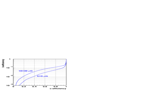
In order to correlate the track extrapolation accuracy to the performances of a jet flavour tagging algorithm at the linear collider, Figure 1 shows the / quark separation capabilities under different assumptions for the track impact parameter resolution.
While the developments of Vertex Trackers from the LEP and SLD experiments to those at B-factories, the Tevatron and the LHC have addressed many crucial aspects, such as radiation hardness, read-out speed and the considerable size increase of the trackers, the impact parameter () resolution, , has not benefited of significant improvements. Limited in terms of multiple scattering at factories and by radiation damage in their closest approach to the beam at hadron colliders, the typical performances are comparable to those achieved at LEP: = 25 m70 m/ GeV/. In order to fulfil its challenging requirements, the TESLA Vertex Tracker aims at significantly improving on the already outstanding SLD VXD3 performances of 8 m33 m/ GeV/ [3]. An improvement to to 5 m10 m/ GeV/ corresponds to a factor increase in charm jet tagging efficiency and a factor increase in beauty jet tagging efficiency at constant mis-identification probability. A precise determination of the track perigee parameters close to their production point also assists in the track reconstruction and improves the momentum resolution for charged particles.
The design of the TESLA Vertex Tracker and the choice of the sensor technology are driven by these requirements, to be achieved within the constraints set by the accelerator induced backgrounds at the interaction region and by the characteristics of the physics events. In the next section, the conceptual design proposed for the Vertex Tracker of the TESLA detector is presented while Section 3 reviews its expected performances. In Section 4, the silicon pixel sensor design, developed to overcome the hybrid pixel sensor limitations in terms of single point space resolution is discussed in details. A road-map of dedicated R&D activity, to validate the concepts presented, concludes.
2 Vertex Tracker Conceptual Design
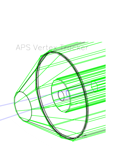
The proposed Vertex Tracker geometry consists of three layers of pixel detectors, providing at least three space points for charged particles with polar angles down to = 0.995. In order to optimise the amount of material traversed by the particles and their angle of incidence on the sensitive plane, the outermost layer is split into a barrel section and a forward crown as shown in Figure 2. A Geant model of this geometry has been implemented in the Brahms simulation program [11] and used for its optimisation and the evaluation of the performances in terms of the impact parameter resolution as discussed in Section 4. The radial position of the innermost layer is set at 1.5 cm by the beam-pipe radius, limited to 1.4 cm due to constraints on the design of the machine collimation system. The outermost layer has been positioned at a radius of 10 cm, fitting the proposed general detector concept that includes two further silicon detector layers located between the Vertex Tracker and the TPC main tracker.
 |
 |
The number of additional intermediate layers is limited by the multiple scattering. Detailed simulation studies, assuming a layer efficiency of 97%, have shown that an optimal configuration consists of one intermediate layer located at 3.5 cm, this layer assisting the extrapolation to the innermost layer affected by the higher occupancy and supplementing a space point close enough to the interaction point in cases of failures on the first layer. Overlaps of neighbouring detector modules provide an useful mean to verify their relative alignment using particle tracks from dedicated calibration runs, taken at centre-of-mass energy.
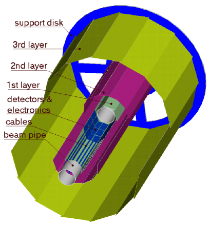
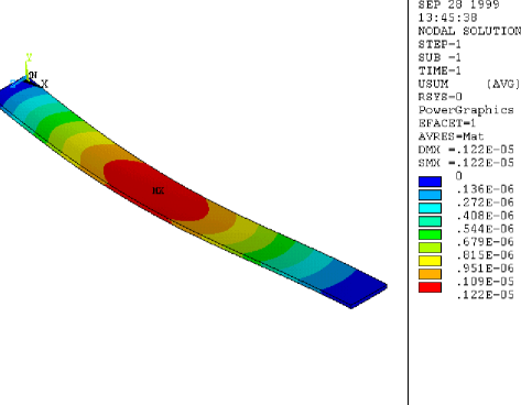
The limitation in the amount of material traversed by charged particles being a major concern to minimise the multiple scattering effects, the pixel Vertex Tracker requires a light support structure able to cope with the load of the detector plaquettes and to ensure their stability to better than their intrinsic single point resolution. The proposed concept for the mechanical structure envisages the use of diamond-coated thin carbon fibre support shells, acting also as heat pipes to extract the heat dissipated by the read-out electronics, uniformly distributed over the whole active surface of the detector. A support plate at each end of the barrel section, made of two thin carbon fibre skins glued together by means of small spacers ensures the needed rigidity and provides a routing for the cables and a support for the forward crown (see Figure 3).
 |
 |
Assuming a power dissipation of 40 W/channel, the total heat flux is 790 W, corresponding to 2600 W/m2, for a read-out pitch of 100 m. In presence of a power dissipation , the temperature gradient along the silicon sensor scales as , where is the distance, the sensor thickness and the thermal conductivity. Owing to its high thermal conductivity (1000-2000 W/m K), small thermal expansion ( -1), high electrical resistivity and large radiation length , diamond is particularly well suited as a heat pipe material. The envisaged cooling scheme consists of a diamond coated heat pipe integrated onto the support layer and heat drains regularly spaced. These drains, consisting of pipes circulating liquid coolant, must be placed every 5 cm along the longitudinal coordinate, except for the innermost layer where they can be placed only at the detector ends to minimise the amount of material. The low duty cycle of the accelerator, makes interesting to consider pulsed power operation to reduce power dissipation.
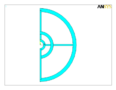
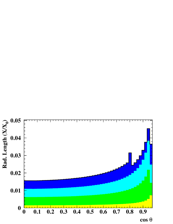
Signals can be routed along the beam pipe and the end-cap disks to the repeater electronics installed between the vertex detector and the forward masks which shield the detector from background. The material budget has been estimated by assuming 200 m thick detectors and back-thinning of the read-out chip to 50 m, corresponding to 0.3 % X0, and the support structure. It corresponds to 1.6 % X0 for the full tracker (see Figure 4 and Table 1).
| Material | |||||
|---|---|---|---|---|---|
| (cm) | (cm) | (cm-1) | (%) | ||
| Beam-pipe | 1.4 | Be | 0.0500 | 35 | 0.15 |
| Sensor+VLSI+Kapton | 1.5 | Si | 0.0250 | 9.4 | 0.37 |
| Support | 1.2 | CF | 0.0240 | 25 | 0.10 |
| Sensor+VLSI+Kapton | 3.5 | Si | 0.0250 | 9.4 | 0.37 |
| Support | 3.5 | CF | 0.0240 | 25 | 0.10 |
| Sensor+VLSI+Kapton | 10.0 | Si | 0.0250 | 9.4 | 0.37 |
| Support | 10.0 | CF | 0.0240 | 25 | 0.10 |
| Total | 1.60 |
The expected data size from the Vertex Tracker has been computed assuming 600 hits per bunch crossing from background sources and 50 charged particles. Taking 16 bits per pixel, this corresponds to 150 kbyte of data from the Vertex Tracker per event.
3 Simulation Studies and Vertex Tracker Performances
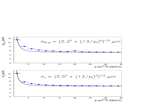
The performances of the pixel Vertex Tracker have been evaluated for and events at = 350 and 500 GeV using full Geant simulation. Tracks reconstructed in the TPC Tesla main tracker have been extrapolated to the detector planes of the pixel Vertex Tracker and a dedicated pattern recognition program has been used to define the association of the recorded hits to the extrapolated tracks. While no attempt has been made to define local track element using only the three layers of the Vertex Tracker, these can be efficiently defined by adding the hits on the two layers of the Silicon Intermediate Tracker, foreseen at radii of 16 and 30 cm. The impact parameter resolution has been studied as a function of the Vertex Tracker geometry, namely the radial position of the second layer, and of the assumed single point resolution . Results are summarised in Tables 2 and 3.
| (m) | (m) |
| () | |
| 4. | 3.7 |
| 7. | 5.3 |
| 10. | 7.5 |
| 13. | 9.5 |
| Asymptotic | Fraction of | |
|---|---|---|
| (cm) | () () | Tracks in Tails |
| 7.5 | 6.0 | 12 % |
| 5.5 | 5.6 | 7 % |
| 3.5 | 5.2 | 4 % |
The efficiency for associating at least two hits to an extrapolated charged particle with 1 GeV/ has been found to be . The track fit has been performed using a Kalman-filter [12] and the impact parameter resolution has been obtained from the estimated covariance matrix. The results obtained assuming = 7 m, are shown in Figure 5.
4 Hybrid Pixel Sensors
The main requirements for the Vertex Tracker sensors may be summarised as follows:
-
•
A single point resolution 7 m and a thickness of m to attain the required impact parameter resolution.
-
•
Time stamping capabilities to identify particles originating from a single bunch crossing, occurring at TESLA every 337 (189) ns at = 500 (800) GeV to reduce the pair background and the number of events overlapped to the products of a collision.
-
•
A sensitive cell area below to keep the occupancy from backgrounds and dense hadronic jets below 1%.
At present, two silicon sensor technologies have the potential to satisfy these specifications: monolithic (Charged Coupled Devices (CCD) and CMOS imagers) and hybrid pixels sensors. Hybrid pixel sensors have the advantage of allowing fast time stamping and sparse data scan read-out, thereby reducing the occupancies due to backgrounds, and of being tolerant to neutron fluxes well beyond those expected at the linear collider. Both these characteristics have been demonstrated for their application in the LHC experiments. However, improvements in the pixel sensor spatial resolution and a reduction of the sensor total thickness are needed. These represent areas of R&D that are specific to this linear collider application. CCD require a complementary development. Their readout speed and radiation tolerance need to be improved, their resolution and thickness being already close to requirements. CMOS imagers have recently appeared and could overcome the CCD limitations while offering similar advantages.
A single point precision at the 5 m level can be obtained by sampling the diffusion of the carriers generated along the particle path and adopting an analog read-out to interpolate the signals of neighbouring cells. Since the charge diffusion r.m.s. is 8 m in 300 m thick silicon, an efficient sampling requires a pixel pitch well below 50 m. At present, the most advanced pixel read-out electronics have minimum cell dimension of , limiting an efficient signal interpolation. Even if a sizeable reduction in the cell dimension may be envisaged by the deep submicron trend in the VLSI development, a sensor design overcoming such basic limitation is definitely worth being explored.
4.1 Detector design and first prototype production
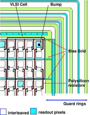
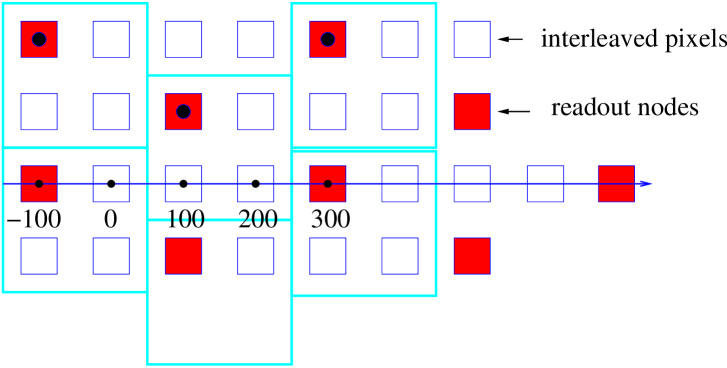
The pixel detector design discussed here exploits a layout inherited from the microstrip detectors [4] where it is assumed to have a read-out pitch n times larger than the pixel pitch. The proposed sensor layout is shown in Figure 6 for n=4. In such a configuration, the charge carriers created underneath an interleaved pixel will induce a signal on the output nodes, capacitively coupled to the interleaved pixel.
In a simplified model where the detector is reduced to a capacitive network, the ratio of the signal amplitudes on the output nodes at the left hand side and right hand side of the interleaved pixel (in both dimensions) should have a linear dependence on the particle position. The ratio between the inter-pixel capacitance and the pixel capacitance to backplane plays a crucial role in the detector design, as it defines the signal amplitude reduction at the output nodes and therefore the maximum sustainable number of interleaved pixels. Recently published results on readout pitch microstrip detectors have demonstrated a resolution for a layout with three interleaved strips ( strip pitch) and [5]. Similar results may be expected in a pixel detector, taking into account that a lower noise is achievable due to the intrisically smaller load capacitance and that the charge sharing on four output nodes makes possible to reconstruct the particle position in two dimensions. Further improvements are possible by sampling the charge carrier diffusion at a smaller pitch.
Prototypes of detectors with interleaved pixels have been designed and manufactured. The layout of one of the structures is shown in Figure 6. A series of guard rings defines the detector sensitive area. A bias grid allows the polarization of the interleaved pixels too; each implant is connected to the metal bias line by polysilicon resistors in the range. A metal layer is deposited on top of the pixels to be connected to the VLSI cell. The backplane has a meshed metal layer to allow the use of an IR diode for charge collection studies. In a 4”, 350 m thick, wafer 36 structures were fit, for 17 different layouts; a VLSI cell of or was assumed and detectors with a number of interleaved pixels ranging between 0 and 3 and different areas were designed.
Ten high resistivity wafers were processed together with an equal number of low resistivity wafers for process control [6]. The technological sequence may be outlined as follows [7]:
-
•
wafer oxidation by HCl gettering, to form a 700 nm thick Silicon dioxide layer;
-
•
Phosphorus glass deposition from a source followed by drive-in in oxidizing environment. The P diffusion was meant to form an layer on the backplane, to guarantee a good ohmic contact with the metal grid;
-
•
pixel and guard ring window opening in the photomask, applying a wet etching technique;
-
•
Boron diffusion, followed by a drive-in process. The resulting junctions were deep;
-
•
high quality thin oxide (200 nm) growth at to define the integrated coupling capacitor on every pixel. This step was carefully monitored to achieve an extremely low density of mobile ion charge;
-
•
polysilicon layer deposition (500 nm thick) and implantation, for the bias resistors. A special high temperature annealing was optimised to obtain the required sheet resistence ;
-
•
resistor pattern definition by photolitography;
-
•
planarisation by BPSG (Boron-Phosphorus-Silicon Glass) chemical vapour deposition, followed by a high temperature annealing;
-
•
resistor coating by photolitography, applying plasma and wet etching technique;
-
•
definition of the contact window between the resistors and the implants. To decrease the contact resistence, Boron implantation was used;
-
•
metal deposition by sputtering a thick Al-Si-Cu layer, patterned by photolitography and plasma etching;
-
•
backside metallisation grid by Al evaporation and plasma etching
-
•
final wafer sintering in Hydrogen at for 20’.
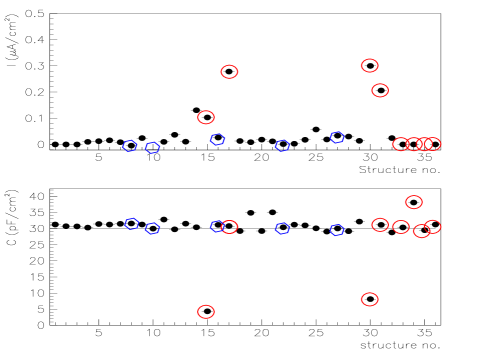
Standard cleaning was performed before each high temperature step. After the processing, two wafers were retained by the factory for a destructive analysis and two others were stored for later use. All of the structures on the available wafers were visually inspected, tested up to and characteristics I-V and C-V curves produced. In Figure 7 the value of the currents and detector capacitances at depletion voltage are shown for all of structures in one of the wafers. In Figure 8 the typical and curves of a good structure are shown.

While the curves behave as expected, the current has a peculiar trend. After a plateau is reached at full depletion, the current increases significantly at V. For most of the structures this is a mild increase, but most of the rejected detectors are characterized by a steep slope, eventually resulting in a breakdown for values of the reverse bias voltage below 100 V. Independent measurements of the guard ring and bias grid current have shown the latter to be responsible for this effect, possibly due to sharp edges where the electric field achieves high values. The average yield over the tested wafers is about 50%; most of the rejected structures feature either an early breakdown or an extremely high leakage current, independent of the applied voltage, correlated to surface defects possibly associated to the plasma etching of the Al pattern. An improvement in the technology sequence, requiring a better planarisation and avoiding plasma etching has been agreed with the manufacturer. Good structures are characterised by a leakage current at the level and backplane capacitances in agreement to the expectations.
4.2 Interpixel and backplane capacitance simulation
and measurements
In order to study the charge collection properties of the proposed detector, a detailed characterization of its electrostatic properties is necessary. In a simplified model, the detector may be reduced to a capacitive network. Each pixel is a node characterised by the backplane capacitance () and the inter-pixel capacitances (), dominated by the couplings to the nearest and diagonal neighbours. The ratio is crucial in the detector design, as it defines the signal amplitude reduction (an effective charge loss) at the output nodes. In order to be able to evaluate the expected behaviour of the prototypes, the capacitances were measured and calculated. Moreover, the obtained values were used as input for a network analysis providing an estimate of the charge loss. Since single pixel capacitances are expected to be at the 10 level, the measurement conditions were optimised as follows:
-
•
The capacitance was measured using a Hewlett-Packard 4280 CV meter, operating at 1 MHz. A cable correction procedure accounting for finite admittances to ground was used. Moreover, an open circuit correction was applied, measuring the capacitance with raised probe tips.
-
•
All pixels along a single metal bias line were set in parallel, isolating the line from the bias grid (see Figure 6). The number of pixels along a line ranges between 64 and 254, depending on the pixel pitch, thus increasing the measured capacitance values to 0.5-2 .
-
•
For every structure, three bias lines were isolated and the capacitance for each of them, for three doublets in parallel and for one triplet was measured. The offset in the linear regression for the capacitance versus the number of lines measured the left-over parasitic contributions after the cable correction.
-
•
For each structure, independent measurements of the total interpixel capacitance and of the sum of the interpixel and backplane capacitance were done.
The numerical estimate is essential to break down the measurements in the single inter-pixel contributions, used to specify the capacitive network. The detector was simply modelled as an electrode matrix facing a metal plane, respecting the pitch, implant width and dector thickness of the different prototypes. The capacitances were obtained solving the Laplace equation with suitable boundary conditions. In fact, setting 1 V on the central pixel and grounding the neighbouring pixels and the backplane, the stored charge on each pixel numerically equals its capacitance with respect to the central pixel, having a backplane capacitance numerically equals to the stored charge on the backplane. The Laplace equation was solved in a pixel matrix, surrounded by a guard ring, with a finite element analysis performed using the OPERA-3D package [8]. The mesh needed by the equation solver was optimised accounting for the physics aspects and the characteristics of the finite element procedure:
-
•
because of the boundary conditions, in our model the potential should always be positive
-
•
the charge neutrality should not be violated, i.e. the sum of the charge on all pixels and on the backplane should be zero.
-
•
a finer mesh had to be foreseen in the regions with higher .
The final optimisation was based on the minimisation of the charge neutrality violation; moreover, this was assumed as a measurement of the uncertainty on the simulation results and defines the errors in the summary table. By changing the the mesh characteristics in the high region, the net effect was estimated to be at the 10% level. The results of measurements and simulation are reported in Table 4.
| chip 1 | chip 2 | chip 3 | chip 4 | |
| Implant width [m] | 100 | 60 | 50 | 34 |
| Implant pitch [m] | 150 | 100 | 75 | 50 |
| Readout pitch [m] | 300 | 200 | 300 | 200 |
| No. of pixels in parallel | 64 | 128 | 126 | 254 |
| Measured | 5995 | 103811 | 9585 | 209830 |
| Calculated | 63060 | 88067 | 69070 | 98040 |
| Measured (I) | 37640 | 39050 | 16045 | 31435 |
| Measured (II) | 4475 | 3685 | 2185 | 1855 |
| Calculated | 47070 | 41090 | 23035 | 21160 |
The consistency of the measurements is checked comparing the value obtained subtracting the measured interpixel capacitance from the measurement of (measurement I in Table 4) and the backplane capacitance from the asymptotic value in the CV curves, normalized by the number of pixels in the matrix (measurement II). The measurement cross check is satisfactory and the comparison with the calculated values is fair for all of the structures but chip 4, where difficulties both in the measurement and in the simulation were expected because of the small pitch. In particular, the maximum number of elements was preventing an optimal interpixel mesh and the extension to a larger pixel matrix, crucial for a proper interpixel capacitance evaluation of pixels with 50 m pitch in a 350 m thick detector. The calculated single pixel main capacitances are summarised in Table 5, together with the maximum charge loss resulting by a network analysis with a dedicated software based on the node potential method [9]. The role of the interpixel capacitance may be stressed referring to chip 4, where the maximum charge loss is reduced to 51% if the measured values are taken.
| chip 1 | chip 2 | chip 3 | chip 4 | |
|---|---|---|---|---|
| Total [] | 26.24.0 | 13.40.9 | 13.82.0 | 9.61.0 |
| [] | 4.40.7 | 2.00.1 | 2.10.3 | 1.50.2 |
| [] | 7.31.1 | 3.20.7 | 1.90.7 | 0.80.2 |
| Max. charge loss | 35% | 32% | 77% | 67% |
4.3 Charge collection studies
The achievable resolution is proportional to the pixel pitch and the Noise over Signal ratio (N/S). If the implant pitch is comparable to the diffusion width, the collected charge at the output nodes will have both the contributions by the direct diffusion and the linear share by the capacitive coupling. In such a case, an improvement beyond the binary value given by the may be expected. The N/S in pixel detectors can easily exceeds 1/100, due to the small detector capacitance. Because of this, an effective signal interpolation may be expected even with signal reduction.
The charge collection properties and the achievable resolution have been directly studied by shining an infrared diode spot on the backplane of a structure with 60 m implant width, 100 m implant pitch and 200 m read-out pitch. At the diode wavelength of = 880 nm, the penetration depth in the silicon substrate corresponds to 10 m. The IR light has been focused to a spot size of 80 m and its position in the detector plane controlled by a 2-D stage allowing to scan the pixel array with micro-metric accuracy. A sketch of the tested structure and the scan direction is displayed in Figure 9. A matrix of 4 7 read-out pixels has been wire-bonded to a VA-1 chip [10]. For each spot position, 1000 events have been recorded. The common mode, pedestal and noise calculation has been initialised for the first 300 events. In the subsequent events light was injected every 10 events, allowing for continuous pedestal tracking. Because of the limited data volume, no on-line suppression has been applied and the data reduction and cluster search has been performed off-line. Results have been averaged over the 70 recorded light pulses, with a peak pulse height corresponding to N/S 1/100 and a maximum charge loss of 40%, in agreement with the network analysis. The charge sharing may be characterised by the function, defined as , where is the pulse height on the reference pixel , normalised to the cluster pulse height.

The function by construction ranges in the [0;1] interval and it has a period equals to the readout pitch. The measured pulse height and distributions are shown in Figure 10, where the reference pixel for the first period has a centre at x = 100 . For the structure under test, the ratio between the spot size and the pitch 0.8 and the experimental curve can be understood as a superposition of the effects due to the diffusion of the charge carriers created by the IR spot on the neighbouring junctions and by the capacitive charge sharing. The parametrisation allows a coordinate reconstruction on an event by event basis and the measurement of the resolution, obtained comparing the laser spot position by the micro-metric stage to the reconstructed values. The results are shown in Figure 11.

In the interleaved pixels, where the charge sharing is most efficient, the resolution approaches , irrespective of the 40% charge loss. On the other hand, when the charge sharing is minimal the resolution degrades to , even with a peak pulse height. According to these results, the binary resolution defined by the can be improved by about a factor 4 for a configuration where the ratio between the charge carrier cloud r.m.s. and the pixel pitch 0.8. A similar scaling factor can be expected for a minimum ionising particle detected by a pixel sensor with pitch, as long as the peak and the charge loss is . This would lead to an intrinsic resolution , matching well the requirements discussed above.
5 Discussion and Conclusions
A Vertex Tracker based on a novel design of hybrid silicon pixel detectors is able to provide performances that are well adapted to the requirements of the TESLA collider while ensuring a significant safety margin against the influence of backgrounds. The ability to identify the individual bunch crossing of a event reduces the occupancy and the confusion rate from pair background and, more importantly, probability of overlap for a event. This ensures that the identification of processes characterised by missing energy and/or heavy flavour jets at small polar angles is not confused for this underlying background [13].
The results reported in this paper conclude the feasibility study of the proposed detector concept and indicate the direction for an intense dedicated R&D programme towards a final detector design. This has to address several crucial issues:
-
•
Sensor development. In order to achieve the desired resolution, a implant pitch detector is needed. The step from is far from being a simple scaling. In fact, because of the limited inter-pixel space, biasing by suitable polysilicon resistors is not feasible. The most promising solution is based on a punch-through mechanism, where very small dots along the metal lines of the bias grid serve sub-matrices of four pixels. Moreover, the design has to be optimised with respect to the inter-pixel to backplane capacitance ratio, with a target charge loss below 50%. A prototype run to validate the possible solutions is planned on a short time scale; this essentially concerns small test structures, meant to be read-out with a low noise microstrip detector electronics chip;
-
•
Electronics chip. On very general ground, each VLSI cell mating the pixel will integrate a low noise and low power charge sensitive amplifier, followed by a CR-RC shaper. Both blocks will be based on the folded cascade architecture with a PMOS transistor, chosen for its lower noise coefficient at its input. The analog information of the pulse height could be efficiently translated into a time-over-threshold, locally digitised on every VLSI pixel cell. Because of the low duty cycle of TESLA, a pulsed mode operation seems very well possible, thus considerably reducing the power consumption. A readout system based on a matrix sparse data scan has to be included in the design, together with time stamping of each pixel hit. The shift-register architecture proposed for the ATLAS pixel detectors could be tailored to the linear collider requirements. An end-of-column logical circuitry would deal with data packing and pipelining. The design of the chip should be optimised with the target of a cell dimension not exceeding , to fully exploit the capacitive charge division mechanism. The development of a dedicated electronics chip being a considerable financial effort, this R&D phase should be considered at an advance stage of the project approval process;
-
•
Technological development. Radiation hardening of the sensor and electronics design, back-thinning of the detector and chip, high density interconnection (flip-chip), cooling, mechanics and system integration require an experimental effort to evolve from the present conceptual design to a fully engineered study that should be planned at a later stage.
Acknowledgements
The R&D activity summarised in this report has been carried out in the framework of the Joint ECFA/DESY Study on Physics and Detectors for a Linear Electron-Positron Collider and it has been supported in part by MURST under grant 3418/C.I. and by the Academy of Finland under the R&D Program for Detectors at Future Colliders grant. We wish to thank R. Brenner, P. Jalocha, C. Meroni, R. Orava, H. Palka, T. Vanhala and K.Österberg for their contributions at different stages of this activity and C. Damerell for his suggestions.
References
- [1] M. Battaglia and K. Desch, to appear in the Proc. of the 5th Int. Linear Collider Workshop, AIP series and hep-ph/0101165.
- [2] G. Borisov, private communication.
- [3] T. Abe for the SLD collaboration, Nucl. Instr. Meth. A447 (2000), 90.
- [4] J.B.A England et al., Nucl. Instr and Meth. 185 (1981) 43.
- [5] M. Krammer and H. Pernegger, Nucl. Instr and Meth. A397 (1997), 232.
- [6] at the Institute of Electron Technology, Warszawa, Poland.
- [7] W. Kucewicz et al., Acta Phys. Pol. B30 (1999) 2075.
- [8] OPERA-3D, software package by Vector Fields Ltd., 24 Bankside, Kidlington, Oxon, OX5 IJE, UK.
- [9] L.O. Chua and P.M. Lin, Computed Aided Analysis of Electronic Circuits: algorithms and computational techniques, Prentice Hall, 1975.
- [10] produced by IDEAS ASA, Veritasveien 9, Box 315, N-1323 H vik, Norway.
- [11] T. Behnke et al., Note LC-TOOL-2001-005.
- [12] M. Elsing, Note LC-TOOL-1999-008-TESLA.
- [13] M. Battaglia and D. Schulte, Note LC-PHSM-2000-052 and hep-ex/0011085.