The Belle Silicon Vertex Detector
Abstract
The silicon vertex detector of the Belle experiment has been built to provide the vertex information of meson decays at the KEKB accelerator. It consists of three cylindrical layers of double sided, double metal silicon sensors read out by VA1 chips. The analog signals are transmitted to a system of fast analog-to-digital converters and are reduced on a system based on Motorola Digital Signal Processors. Performance during the initial data taking period and a brief description of the upgrade plan are also presented.
keywords:
Belle, KEKB, B-factory, Silicon vertex detector(To appear in the Proceedings of the 4th International Symposium on Development and Application of Semiconductor Tracking Detectors, March 22 - 25, 2000 Hiroshima, Japan )
1 Introduction
The Silicon Vertex Detector (SVD) of the Belle experiment [1] at the KEKB accelerator [2] has been built to provide vertex information from precision measurements of charged tracks in the vicinity of the interaction point. Because the KEKB is an asymmetric collider with 8 GeV and 3.5 GeV beams, a pair of and mesons, produced nearly at rest at the center of mass system (CMS), is boosted along the beam direction with a Lorentz boost factor of . Therefore, in designing the SVD a special emphasis is placed on the precise measurement of the (boost direction) coordinate. The typical separation between and decays at the KEKB is m and we find, based on the simulation, the resolution of m in meson decay vertex measurement is sufficient to detect a possible asymmetry in the proper time interval distribution for decays of pairs. This asymmetry signals -violation in the meson system when one of the neutral mesons decays to a eigenstate.
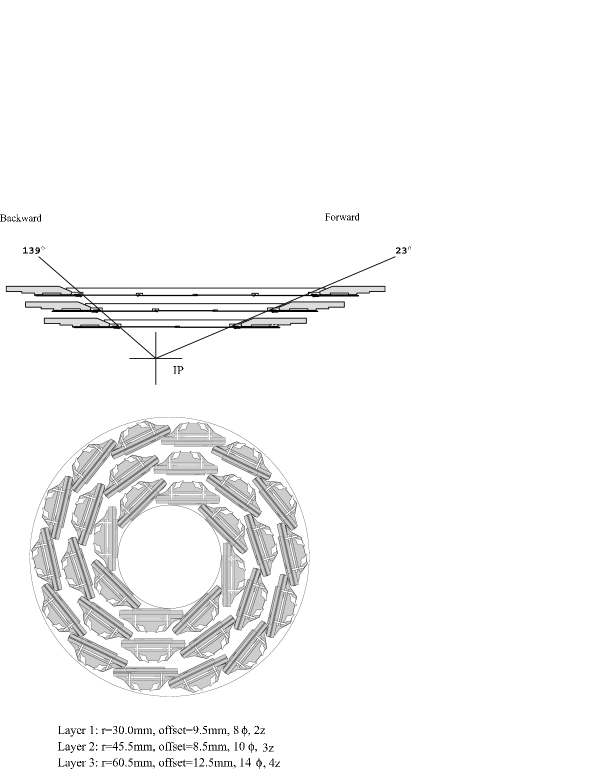
The SVD consists of three concentric cylindrical layers of silicon sensors with two orthogonal-coordinate readouts. The vertex resolution for low momentum tracks is dominated by multiple scattering in a material before the SVD plus the first SVD layer. Figure 1 displays the geometrical layout of the SVD. The radii of the three layers are mm, mm and mm. The SVD covers the polar angle range of corresponding to of the solid angle in the CMS. There installed is a mm-radius beryllium beampipe with two mm-thick walls allowing helium gas flow to cool the beampipe. A 20 m gold foil is glued on the inner concentric cover consisting of carbon-carbon material to protect the SVD from soft Xrays produced in the beampine. The material before the first SVD layer amounts to of 1 radiation length.
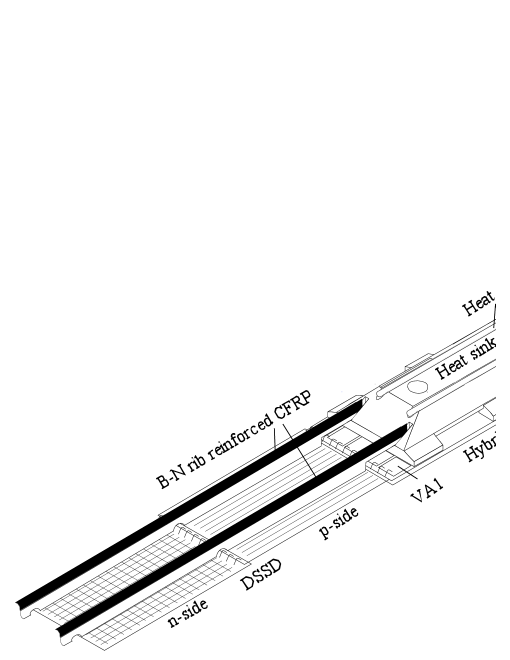
The first layer is formed from 8 “ladders”, each of which contains two double-sided silicon strip detectors (DSSDs) which are read out separately. The second layer is formed from 10 ladders, each containing 3 DSSDs. Two of 3 DSSDs are connected to make a single two-sensor unit, in which p-strips on one DSSD are wire-bonded to n-strips on the other DSSD to minimize a noise in a channel. The third layer is formed from 14 ladders, each containing 2 two-sensor units. A full ladder consists of DSSDs, aluminum nitride hybrids at each end, glued with an aluminum nitride heat sink containing two heat pipes and CFRP reinforced boron nitride ribs glued across DSSDs and the heat sink, as shown in Fig. 2. The DSSD, HPK S6936, was originally fabricated for the DELPHI vertex detector by Hamamatsu Photonics. It has an active area of with a thickness of . The strip pitch for a p(n)-side is m and the readout pitch is m. This DSSD contains integrated coupling capacitors and, therefore, the strips are AC-coupled to preamplifiers. It utilizes a double metal structure to read out n-strips. The total number of readout channels of the SVD is 81920. A bias voltage of 75V is supplied on n-side.
Each hybrid is made by gluing two identical aluminum nitride boards, each containing five 128-channel VA1 chips [3] providing 640 readout channels per board. The VA1 chip fabricated by 1.2 m feature size process contains preamplifiers, shapers and track-and-hold circuits that capture the analog pulse-height information of each channel. The peaking time of the shaper is set to s to match the trigger latency. When the system switched from track- to hold-mode the stored analog information for each channel is sequentially routed via an on-chip analog multiplexor to a system of fast analog-to-digital converters (FADCs) [4]. Event buffering and zero data suppression are performed using Motorola Digital Signal Processors (DSPs) in the FADC module.
2 Basic Performance
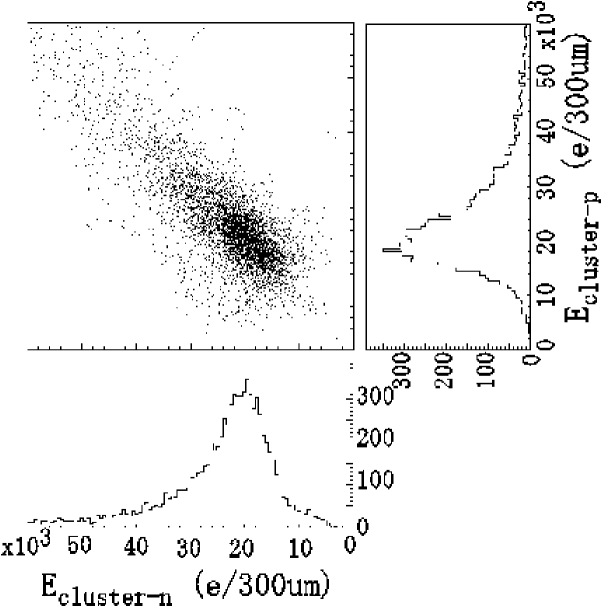
The distributions of minimum ionizing particles for p-side and n-side, together with the correlation between signals from two sides are shown in Fig. 3. The values are calculated by summing all signals (above threshold) which belong to the same track and by normalizing to the same track length (i.e., 300 m). The signal peaks at and for p-side and n-side, respectively, while the electronics noise is found to be for p-side channels, for n-side channel and for p-n combined channels in which a p-strip and an n-strip are connected. Therefore, Signal-to-Noise (S/N) ratio is well above 10. The strip yield for each layer is found to be , and for 1st, 2nd and 3rd layers, respectively. The loss of strips includes failure of hybrids and a few failed coupling capacitors. Since the installation in August 1999, the SVD has been functioning stably. The occupancy of the SVD is at the luminosity of . For hadronic events we find of tracks reconstructed by the Central Drift Chamber (CDC) have corresponding hits in the SVD. The internal alignment of the DSSDs and the SVD-CDC relative alignment have been performed using cosmic rays taken with and without beams in the KEKB. In order to illustrate the so-far achieved alignment we summarize in Table 1 resolutions of track helix parameters111 A charged particle track is expressed as: , , , . compared with the values for the perfect alignment, predicted by Monte Carlo simulation. We note that the resolutions are mostly determined by the SVD internal alignment performance, while the resolutions depend on the CDC track resolutions as well.
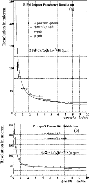
Figure 4 shows impact parameter resolutions, , for and directions measured using cosmic rays, Bhabha events and processes. We obtain
where and are momentum in and velocity divided by of the particle, and is the polar angle from the beam axis. The resolution in a measurement of the distance between two vertices of leptons originating from a particle can also infer the resolution of the coordinate measurement. Here, each vertex is calculated by finding an intersection between a lepton track and the beam axis. We find , while Monte Carlo predicts .
3 Physics Examples
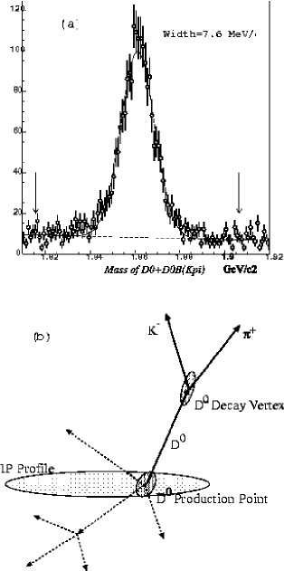
In order to demonstrate the overall performance of the SVD, we present preliminary results of and meson lifetime measurements based on the first data collected during the initial data taking period [5]. We reconstruct mesons in the decay mode . Charged tracks forming a candidate are required to be well-reconstructed in the tracking system and to originate from a common vertex. Kaons are positively identified in the particle ID system [6]. In order to avoid bias due to meson lifetime, mesons originating from mesons are removed by requiring mesons have a minimum momentum of in the rest frame. Figure 5(a) shows the invariant mass distribution of decays. By fitting the distribution with a Gaussian for the signal plus a linear function for the background, we find the width of the signal distribution to be and the number of signal events to be . The background fraction is calculated from the same fit and is about under a signal peak (the region within ).
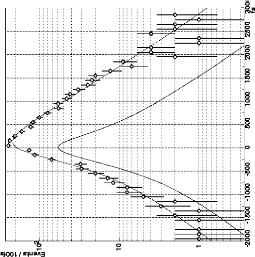
As illustrated in Fig. 5(b) the lifetime of the charmed meson is computed from the flight distance between the reconstructed vertex and the interaction point(IP) determined for each KEKB beam fill. The profile of the IP is known to have, from the machine optics and the beam size monitoring information, along the beam direction , and , and in the direction perpendicular to the beam direction. The flight length is measured in the plane to take advantage of the small IP size in the plane. The projected decay length of the meson is calculated from the momentum , the decay vertex , and the production point reconstructed by extrapolating the momentum back to the IP profile: . The proper time is, then, calculated using the mass, , as . The meson lifetime is extracted from the proper-time distribution with an unbinned maximum likelihood method. The detector resolution is mostly described by a single Gaussian with a small correction for events which might have undergone a hard multiple Coulomb scattering and/or have wrong CDC-SVD hit associations in the track reconstruction program. Figure 6 shows the fit to the proper time distribution. The preliminary result for the lifetime of meson is where the error includes only the statistical error. This is in good agreement with the PDG value of fs.
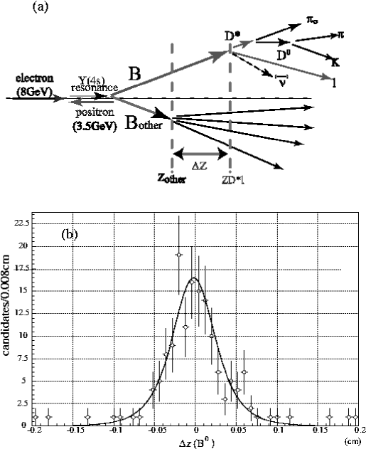
The meson lifetime is extracted from the measurement of the separation of and decays, , in the direction. We first reconstruct , where decays to followed by either one of , , decays. The decay vertex of is determined using the reconstructed momentum and the lepton track. We, then, determine the decay vertex requiring all the remaining tracks in the same event, except for tracks originating from decays and tracks with large impact parameters, form a common vertex. Figure 7(a) illustrates the vertex reconstruction of events. The distribution of with the fit result is shown in Fig. 7(b). The fitted function consists of the expected distribution smeared with the detector resolution. We obtain the result of ps, while the resolution in is found to be . The result is consistent with the PDG value of ps.
4 Upgrade Plans
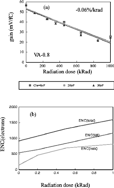
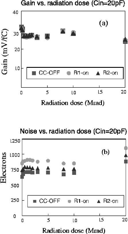
The current SVD readout chips have limited radiation tolerance. The -technology VA1 chip is not based on a radiation-hard technology and stops functioning after a -ray dose of krad. With the current radiation level observed at the KEKB, this corresponds to an integrated luminosity of . We have been developing a frontend IC which stands radiation dose of more than 1Mrad by taking advantage of the thinner gate-oxide layers used in sub-micron CMOS processes. Because the threshold shift in a MOS transition scales as the square of the thickness of the gate oxide layer, which in turn is proportional to the FET channel width or equivalently to the feature size of the process being used, one expects the radiation tolerance of the IC scales as the inverse square of the feature size. One expects that a m process IC is four times more radiation-tolerant than a m process IC. We have fabricated two versions of VA1 chips, one with AMS m technology and the other with AMS m [7]. Figure 8(a) shows gain versus radiation dose for AMS m technology VA1. The gain decrease rate is found to be /krad. Figure 8(b) shows the equivalent noise count versus radiation dose. Based on these measurements we conclude the m VA1 chips are radiation tolerant up to Mrad. The new SVD built with these VA1 chips is scheduled to be installed in summer 2000. The AMS m VA1 exhibits the excellent radiation hardness as shown in Fig. 9. It is tolerant up to 20 Mrad. The SVD based on this m VA1 chips is also being planned.
5 Conclusion
We have successfully built the SVD for the Belle experiment at the KEKB. Preliminary measurements of lifetimes of and mesons show it is performing as designed. We have developed radiation-hard VA1 chips, based on a sub-micron process technology, which will be applied to the immediate upgrade of the SVD.
6 Acknowledgments
The author is grateful to the conference organizers for their hospitality, and indebted to colleagues of the Belle SVD group for their help in preparing the talk. This work is supported by a Grant-in-Aid for Scientific Research on Priority Areas (Physics of CP violation) from the Ministry of Education, Science and Culture of Japan, and by the Japan-Taiwan Cooperative Program of the Interchange Association.
References
- (1) [1] Belle Collaboration, Technical Design Report, KEK Report 95-1, 1995.
- (2) [2] KEKB B Factory Design Report, KEK Report 95-7, 1995.
- (3) [3] E. Nygard et al., Nucl. Instrm. and Meth. A301(1991)506. O.Toker et al. Nucl. Instrm. and Meth. A340(1994) 572.
- (4) [4] M. Tanaka et al., Nucl. Instrm.and Meth. A432 (1999)422.
- (5) [5] H. Aihara, “Physics Results from Belle,” Proceedings of the 3rd International Conference on B Physics and CP Violation, December 3-7, 1999, Taipei, Taiwan.
- (6) [6] T. Iijima, “Kaon Identification in Belle,” ibid.
- (7) [7] M. Yokoyama, “Test results of VA1 fabricated by sub-micron technology,” This proceedings.
Table 1: Track helix parameter resolutions compared with Monte Carlo predictions for perfect alignment (mrad) dz tan Data 28.0 0.747 2.63 42.1 0.973 Perfect (MC) 19.4 0.503 1.73 34.4 0.891
.