![[Uncaptioned image]](/html/hep-ex/0002044/assets/x1.png)
The H1 silicon vertex detector
Abstract
The design, construction and performance of the H1 silicon vertex detector is described. It consists of two cylindrical layers of double sided, double metal silicon sensors read out by a custom designed analog pipeline chip. The analog signals are transmitted by optical fibers to a custom designed ADC board and are reduced on PowerPC processors. Details of the design and construction are given and performance figures from the first data taking periods are presented.
1 Introduction
The Central Silicon Tracker (CST) of the H1 experiment at the HERA electron-proton collider of DESY has been built to provide vertex information from precision measurements of charged particle tracks close to the interaction point. It consists of two concentric cylindrical layers of silicon sensors with two-coordinate readout allowing the identification of heavy-flavour particles with decay lengths of a few hundred micrometers [2]. The production cross section for charmed quark pairs at HERA is of order 1 b which offers a rich field of physics topics [3] that can be exploited once a large number of charm events are tagged by the vertex detector. In addition, the production of -quarks can be studied. The cross section is smaller by about two orders of magnitude but the longer lifetimes of B-mesons lead to a more efficient tagging. The bulk of the heavy quarks are produced close to threshold such that their decay products have an average transverse momentum around 0.7 GeV/c. The vertex resolution is dominated by multiple scattering and the amount of material in front of the second silicon layer must be kept at a minimum. This led to a design with all readout electronics arranged at the ends and a central region consisting essentially only of active sensor material.
Space for the installation of the CST was obtained by reducing the beam pipe radius from 95 mm to 45 mm, which was the minimum radius required to protect the vertex detector from the direct and backscattered synchrotron radiation emitted by the electron beam.
The CST has been fully operational since the beginning of the 1997 running period. It complements the original central tracking detectors of H1, which consist of the main jet-cell drift chamber extending from 20.3 cm to 84.4 cm in radius, interspersed by a drift chamber for z-coordinate measurement between 46 cm and 48.5 cm radius, and an inner z-drift chamber between 17.35 cm and 20 cm radius. A superconducting coil provides a uniform magnetic field of 1.16 T. Further details can be found in [1]. Simultaneously to the implementation of the CST the tracking of electrons scattered at small deflection angles was made possible with the installation of initially four and, since 1998, eight disks of silicon sensors in the Backward Silicon Tracker (BST). The BST [4] uses the same frontend ASICs and the same readout electronics as the CST.
In the following section the layout and mechanics of the CST are described. Section 3 covers the frontend components, i.e. the sensors, the readout and control chips, the hybrid and the optical link. The on-line data processing and monitoring of slow control data is covered in section 4. The off-line track linking and the alignment procedure are explained in section 5. The performance numbers achieved so far are presented in section 6.
2 Layout
2.1 Geometry
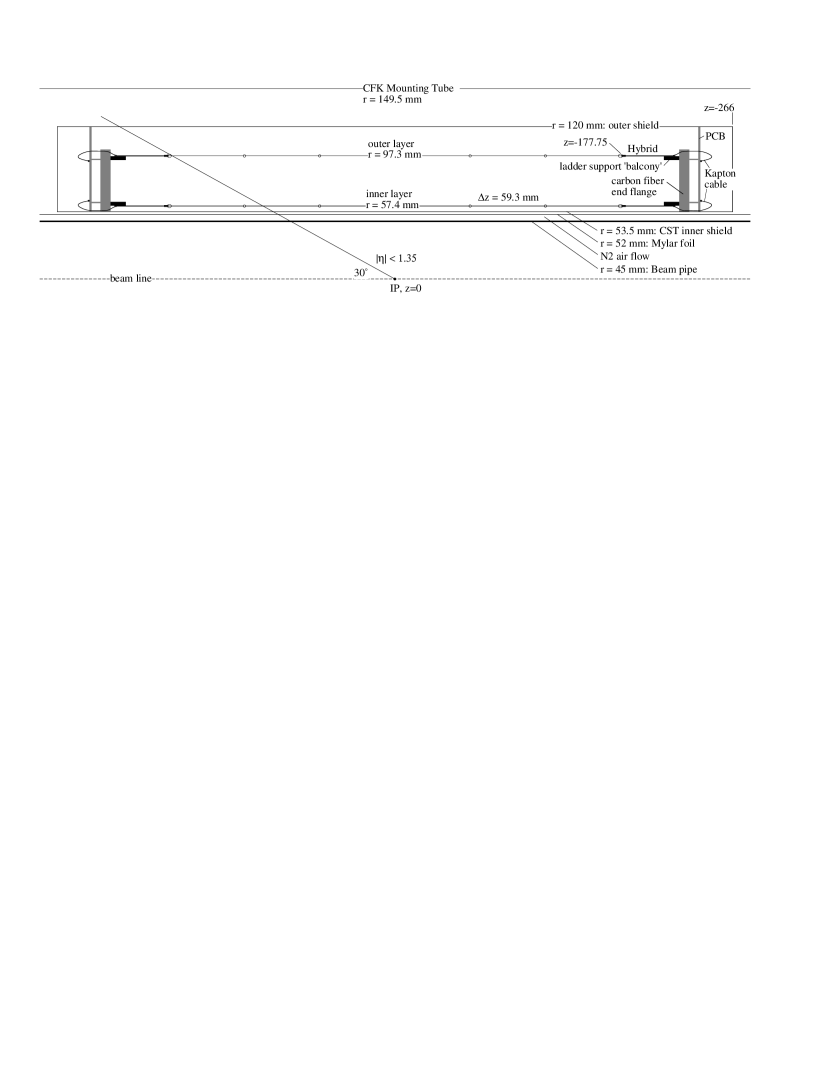
The radial space available for upgrading the H1 experiment with a vertex detector was limited on the outside by the first MWPC trigger chamber starting at 15 cm radius. On the inside the space was restricted by a beam pipe radius of 4.5 cm as required by the synchrotron radiation environment, and by an additional 7 mm wide gap for cooling of the beam pipe with nitrogen gas flowing inside of a Mylar foil. The beampipe was initially made of aluminium with a wall thickness of 1.7 mm. It was replaced in early 1998 by a beam pipe made of 0.15 mm aluminium and 0.9 mm carbon fiber.
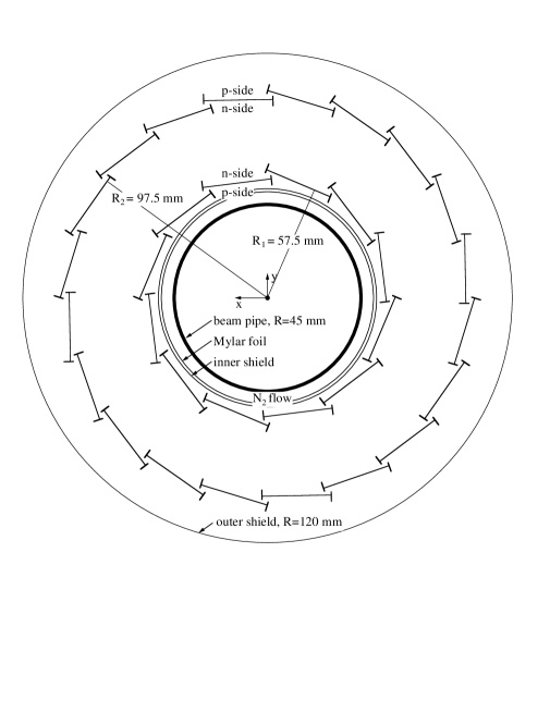
The two layers of the CST are formed from 12 and 20 faces at radii of 5.75 cm and 9.75 cm, respectively, as shown in figure 1. One face or ’laddder’ consists of six silicon sensors and aluminium nitride hybrids at each end (see figure 2). A double layer of carbon fiber strips with a total thickness of 700 m and a height of 4.4 mm is glued to the edges. The carbon fiber strips were specified with a Young’s modulus of at least 400 000 N/mm2. The gravitational sag of a full ladder when supported at the outer ends was measured to be less than 6 m.
The positions of the ladders in a layer are shifted tangentially to ensure an overlap in r- of adjacent active areas, which amounts to 1.5% in the inner layer and 2.1% in the outer layer. The active length in is 35.6 cm for both layers, see figure 2, to be compared to the length of the luminous region at HERA with an rms width of 10 cm. The coverage of the outer layer extends over units in pseudorapidity for tracks emerging from the origin. The length is a compromise between rapidity coverage and preamplifier noise which is proportional to the length.
2.2 Mechanical Frame and Installation
The ladders are mounted on small balconies extending from carbon fiber endflanges (see figure 3). These balconies contain a high precision metal pin used to position the hybrids at laser-cut holes. Two small screws on each hybrid are used for fixation.

The carbon fiber endflanges house a circular cooling water pipe for each layer with copper-tin sheets attached which reach into the balconies and thus provide thermal contact with the hybrids. The power dissipation of the CST is 50 W [11]. This power is removed with 12oC cold water at a total flow rate of 2/min. The equilibrium temperature rises from 19oC for the unpowered detector to 28oC during operation.
The endflanges are split in the horizontal plane (see figure 3) allowing for the installation around the beam pipe. The lower half of the CST rests on three carbon fiber legs in a carbon fiber support tube (see figure 4) which is attached to the innermost tracking chamber of H1. The upper half of the CST rests on the lower half.

Upon installation the two halves of the CST are first mounted on rail extensions around the beam pipe about 2 m from the final position. A split service tube enclosing power leads, optical fibers and cooling pipes is equally mounted behind the CST and connections between the CST and the service tube are made. Then the CST and the service tube slide on straight carbon fiber rails, integrated in the support tube, into the final position, which is defined by spring-loaded end stops.
The service tube, depicted in figure 4, has a radial width of only 2 mm and surrounds the backward silicon tracker [4]. The wall of the service tube is made of a sandwich of 20 m aluminium foil, 2 mm Rohacell [18] with grooves for the aluminium power leads and another 20 m aluminium foil. At the edges of the half-shells flat cooling pipes of 2 mm height are incorporated. Cable connectors and voltage regulators are integrated in the service tube endflange facing away from the CST.
3 Frontend Components
Each ladder consists of two electrical units, called half-ladders. A half-ladder consists of three silicon sensors of 300 m thickness, and a ceramic hybrid of 635 m thickness carrying the front-end electronics, see figure 5.
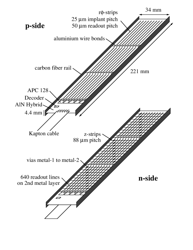
The silicon sensors have 12 m wide strip implants on both sides. The strips on the p-side, where holes are collected, are oriented parallel to the beam direction and have a pitch of 25 m. Every second strip is read out for a measurement of the -coordinate at a known radius. The intermediate strips contribute to the signal by capacitive coupling and improve the position resolution . The implants on the n-side, where electrons are collected, are rotated by 90o with respect to the p-side strips and have a pitch of 88 m for a measurement of the z-coordinate. Every n-strip is read out by means of a second metal layer integrated on the sensors. There are 640 readout lines on each side of a sensor, which are daisy-chained by aluminium wire bonds between sensors, and connected to preamplifier ASICs on the hybrid. This arrangement leads to an effective strip length of 17.3 cm on the p-side and to a three-fold ambiguity for the z-coordinate on the n-side. The insensitive region at each end of the sensors and a gap of 300 m between the sensors lead to a coverage in the z-direction of 97 % on the p-side and 95 % on the n-side. In total, the CST contains 64 half-ladders with 192 silicon sensors and 81 920 readout channels.
3.1 Silicon Sensors
High resistivity n-type silicon ( kcm) was obtained as a 100 mm diameter boule from Wacker Chemitronic [7]. Cutting of 300 m wafers and polishing of both sides was performed by Siltronix [9]. The wafer processing was performed at CSEM [8], where the basic double sided process was extended to provide a second metal layer over a 5 m thick deposited oxide on the n-side. The contact vias between metal-1 and metal-2 have a drawn opening of m2 and proved to be very reliable. Using contact chain test structures a failure rate of less than was determined (all CST sensors together contain vias). The masks for the 14 layers in this process were designed by the collaboration.
The CST sensors have a full size of cm2, such that two sensors can be produced on a 100 mm diameter wafer. The strip implants are DC coupled to the metal-1 layer on both sides. Early prototypes were AC coupled but showed [6] a defect rate for the coupling capacitors on the n-side that led us to resort to DC coupling. The intermediate strips on the p-side are biased from a common guard ring across a punch-through gap covered by a FOXFET gate. With gate and guard at ground potential and positive bias voltage applied to the n-side the intermediate strips float at 4 V, with a uniformity of about 1 V on individual detectors and also between different wafers and different production lots. We are currently not supplying a dedicated gate voltage, although this option is available in the cabling scheme. The active area on the p-side (the junction side) is surrounded by a multi-ring guard structure with floating gates, that leads to a gradual increase of the surface potential from 0 V at the innermost guard ring to the full bias voltage at the edge. The carbon fiber strips glued to the sides of the sensors are floating at bias potential.
Each strip on the n-side is surrounded by a narrow ring of p-implant to provide the necessary interstrip insulation. The n-side can only be operated at full depletion, which requires between 30 V and 50 V for the installed sensors. Although the strips are DC coupled to the metal-1 layer and all n-side strips are read out we kept the accumulation channel structure which provides a high resistance connection to a common guard ring [6]. The sensors can then be fully depleted for a measurement of the total leakage current with only 2 test probe contacts, instead of having to contact 640 strips on each side.
Detectors with less than 6 A of leakage current at 50 V bias where selected. Further tests prior to assembly included sparse measurements of the punch-through voltage on the p-side and the conductivity of the metal-1 to metal-2 vias on the n-side. The depletion voltage was determined at several positions on each sensor by a measurement of the interstrip resistance on the n-side. Finally, each sensor was scanned under a microscope for shorts or interrupts in the metallization. Sensors with more than 6 defective strips on either side were rejected. The final yield of accepted sensors was 62 % for 9 production lots.
The interstrip capacitance of one strip with respect to its six closest readout neighbours was measured as 1.5 pF/cm on the p-side, for 50 m pitch and 12 m implant width. On the n-side a value of 19 pF was measured for the capacitance of one strip with respect to the other 639 strips on a sensor. It is dominated by the overlap capacitance between metal-1 and metal-2 lines across the 5 m oxide layer.
3.2 Analog Pipeline Chip
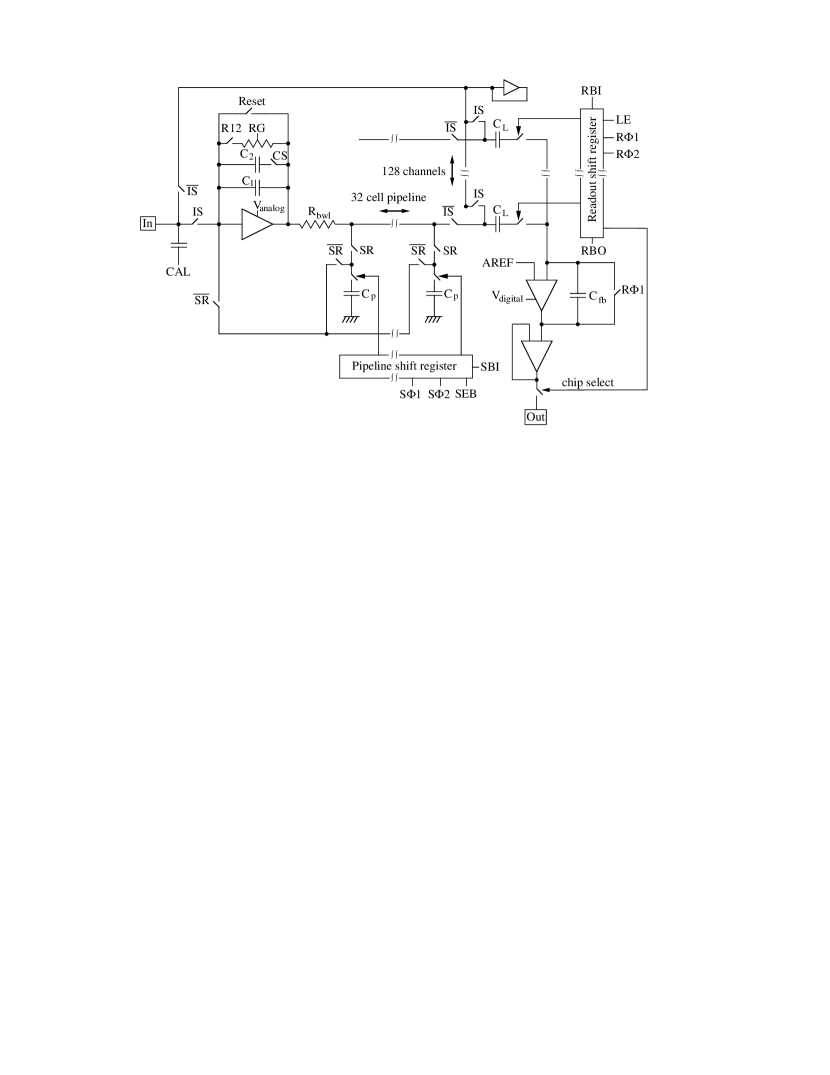
The time between bunch crossings at HERA is 96 ns while the H1 level-1 trigger decision arrives after 2.4 s. Therefore all front-end readout systems have to store the signals from at least 25 beam crossings in a pipeline. For the H1 silicon detectors an integrated preamplifier and pipeline chip with multiplexed readout for 128 channels has been developed [15] and fabricated in 1.2 m CMOS technology [16]. Figure 6 shows the schematics of the APC128 readout chip. The various external signals, internal switches and circuit components are explained in the following sections.
3.2.1 Preamplifier
The charge sensitive input amplifier consists of a single push-pull inverter stage which offers minimal noise for a given power dissipation. The open loop gain is about 150, which, together with a (parasitic) feedback capacitance C pF, leads to a Miller capacitance that is not much larger than the input load capacitance, especially on the n-side. The equivalent noise charge was measured as
at 0.3 mW power dissipation and sampling at 10 MHz [17]. The risetime of the amplifier with the detector load was measured to be 100 ns for the p-side and 150 ns for the n-side. Due to DC coupling between sensor and chip the preamplifier must absorb the strip leakage current through its feedback resistor (), which is adjustable by an external voltage and set to a value of about 1 M. Consequently the signal decay time is 450 ns which is sufficient to avoid pile-up at HERA. Leakage currents of up to several hundred nA per strip can be tolerated before the preamplifier runs into saturation.
Several switches are used to control the preamplifier. During data taking the input select switch IS is closed, connecting the preamplifier input to a strip. The Reset switch is open and the switch R12 is closed, activating the feedback resistor RG. By closing switch CS a second feedback capacitor C2 can be added, which can be used for analog signal processing [15] and calibration purposes. At H1, however, this feature is not used during regular data taking. The sample/read switch SR connects the preamplifier output to the switched capacitor analog pipeline. The preamplifier can be tested by applying a voltage step to the CAL input. The CAL pulse is reduced internally by about a factor 35 (not shown in figure 6). The CAL capacitors of four neighbouring channels have nominal values of 40, 80, 120 and 160 fF, which leads to a charge injection corresponding to one to four minimum ionizing particles in 300 m of silicon for a 3 V external test pulse.
3.2.2 Pipeline
The output voltage of the preamplifier is captured on one of 32 capacitors ( pF) that form the analog pipeline for each channel. The capacitors are cyclically switched under the control of a common shift register operating at the HERA frequency of 10.4 MHz. A sample clock made from two signals ( and ), phase shifted by 50%, with flat tops and common low periods of at least several ns is required. The shift register is cleared by setting both clock signals high and requires a couple of nanoseconds per cell. The sample bit () must be refreshed externally every 32 cycles.
3.2.3 Re-read and offset subtraction
The pipeline is stopped externally at a level-1 trigger signal. The H1 second level trigger may reject an event after a decision time of 22 s, upon which the sampling phase is resumed. An L2 accept decision starts the readout, for which the APC must be put into a different mode. First, the input is disconnected from the silicon sensor by opening the input select switch IS. This automatically closes the switches which connects all 128 strips to an extra preamplifier in auto-feedback configuration to absorb the leakage current during the readout phase. Secondly, the sample/read switch SR is opened, and the switches are closed, which disconnects the write lines to the pipeline capacitors and prepares the read lines. Thirdly, the reset switch is closed for a few s to bring the preamplifier into a well-defined state.
The APC employs a self-re-reading architecture where the pipeline capacitors are read back by the same preamplifier that wrote them. The pipeline cell associated with the triggered event is reached by advancing the sample bit in the shift register from the stopped position, refreshing it externally, if necessary. The sample enable bar switch SEB is open during this phase in order not to discharge the pipeline capacitors while advancing the sample bit. The selected capacitor is then read back through the preamplifier by closing SEB. The charge stored is amplified by a factor and copied to the latch capacitor CL. A second and a third sample of the pulse stored in the pipeline is also read back and added to the charge on CL, which improves the signal-to-noise ratio by effectively increasing the integration time.
The latch capacitors are necessary to separate the preamplifier section of the APC, which operates at a voltage of about 2 V (Vanalog), from the readout section, that operates at 5 V (Vdigital). They also provide intermediate storage of the signals during the serial readout. Thirdly, they are used to perform an on-chip pedestal subtraction. During sampling and up to this point the right plate of the latch capacitor CL was connected to the readout amplifier by closing the latch enable switch LE and permanently filling the readout shift register. Switch LE is now opened, which captures the signal charge on the right plate. The left plate is cleared by resetting the preamplifier. The pedestal is taken from three pipeline capacitors just before the event occurred and read back with the same procedure as the signal. With the R12 and Reset switches open, the preamplifier maintains the pedestal potential, including any shift of the operating point due to leakage current, at the left plate of CL. When the readout amplifier is connected to CL again the difference between pedestal and signal is transferred.
3.2.4 Serial readout
The serial readout is controlled by a shift register which again requires a two-phased clock signal (R and R) and a readout bit RBI. The right plates of the latch capacitors CL are sequentially connected to the readout amplifier having a feedback capacitance Cfb, which provides an amplification of about 10. A readout speed of 4 MHz can be reached, if the analog output of the APC is immediateley followed by a driver amplifier. For the CST it is limited to 1.6 MHz by the trace capacitance on the ceramic hybrid carrying the APC. The readout of 10 APCs is multiplexed by feeding the readout bit appearing at RBO to the RBI input of the next chip. A chip select mechanism ensures that only one APC at a time connects to the common readout line. The full serial readout cycle for 1280 channels requires 1.1 ms, which is just sufficient in H1.
3.2.5 Decoder Chip
The APC requires 13 external signals, of which only the clock and sample bit signals are fast, while the others change only when switching from sampling to readout mode. The number of external clock and control signals that need to be brought to the front end can be reduced to four by using a dedicated Decoder chip [11]. The desired state of all APC switches is first loaded serially into registers on the Decoder chip and then applied to the APC. The fast clock and data signals are passed directly either to the pipeline or the readout shift register. Further functionalities have been added to the Decoder Chip: It can generate a test pulse for the signal at any of the 32 pipeline buffer positions. It has a 7-bit DAC which drives a current source for the APC preamplifiers allowing to define the operating point externally. Finally, two stabilized and one temperature dependent voltage can be connected to the readout line, which allows a gain calibration and temperature monitoring. The Decoder chip was also fabricated in 1.2 m SACMOS technology [16].
3.3 Hybrid and Optical Readout
Aluminium nitride was chosen as the substrate of the ceramic hybrid for its excellent heat conductivity W/Km, compared to W/Km for aluminium oxide. The hybrids have a size of mm2 and have two conductor layers on each side. Connecting vias and holes for fixing screws are cut by laser [10]. One side contains a blank area of mm2 for heat contact with the mechanical support structure. Five APCs and one Decoder are mounted on each side of the hybrid and connected by aluminium wire bonds. The hybrid carries current sources for the APC preamplifiers, a voltage reference for gain calibration, a temperature monitor and drivers for the analog output signal. The back side of the hybrid, which supplies the n-side of the silicon sensors, is floating at bias voltage potential. The digital input signals are transferred across small capacitors which separate the DC levels. A thin Kapton cable with 20 lines is glued and wire bonded to the hybrid and connects to a ring-shaped printed circuit board (endring print) mounted on the CST endflanges.
The digital control signals and the analog readout are transferred by optical fibers [11] over 34 m between the detector and the electronics trailer, which minimizes the amount of cable material introduced into the center of H1 and prevents electromagnetic interference. Receivers for a set of four digital control signals are mounted on four endring prints, each serving one quarter of the CST. The analog signals are transmitted by a total of 64 LEDs, which are connected to sockets located on the endring print. One LED transmits the serial readout of either 1280 p-side channels or 1280 n-side channels from two neighbouring half ladders. The LEDs for the n-side are floating at the bias voltage potential.
4 Readout and Monitoring
The frontend system is connected via 34 m optical fibers and electrical cables to the readout electronics in the electronics trailer. The fibers and cables are interrupted twice by connector boards allowing the installation of the CST and access to other H1 detector components.
4.1 Readout and on-line Data Processing
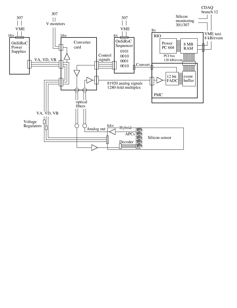
Figure 7 shows schematically the components of the readout and monitoring system. All electrical and optical leads arrive at a converter card located in the electronics trailer. It contains LED drivers for the digital control signals and PIN diode receivers for the analog optical signals. It also provides passive filtering for the frontend supply voltages and the detector bias voltage. The supply voltages are further stabilized by active voltage regulators placed on the service tube about 1 m from the detector. These regulators can be adjusted from the converter cards allowing to optimize the working points individually for units consisting of pairs of ladders (four half-ladders). Finally, the converter cards include circuits for monitoring temperatures, voltages and detector leakage currents. If a given temperature limit is exceeded or if the cooling system fails, the converter card autonomously operates relays switching off the supply voltages to the frontend.
The frontend voltages are generated in VME modules called OnSiRoC [12]. The bias voltages are programmable in the range 0 V to 108 V. The OnSiRoC is interfaced to the H1 central trigger and generates the control sequences required to run the APC128 chips. A typical sequence occupies 32 kB in memory and is loaded through VME. A fast compiler was developed on a Macintosh platform which allows to generate the sequences from higher level building blocks.
The digitisation of the analog signals is performed on a custom-built PCI-bus mezzanine card [13] using 12 bit FADCs. The CST creates about 1 MB of raw data per event, which is transferred via PCI bus into 8 MB memories on RIO2 VME cards [14]. A hit-finding and zero-suppression algorithm is executed on PowerPC 604 RISC processors operating at 96 MHz. The algorithm first determines and subtracts an average baseline for groups of 128 channels located on individual frontend chips. The event-to-event variation of this common baseline is comparable to the single-channel RMS noise. In a second loop over the data the individual pedestals are subtracted and hit searching is performed. A hit is defined as a contiguous group of channels, each with an amplitude greater than its RMS noise, and with an integrated pulse height of at least four times the average single channel noise. The hits are copied to an output buffer. In a third loop the pedestals are updated, using a running average for each channel and each APC pipeline buffer, and variances for individual noise determination are accumulated, except for those channels contributing to a hit. Further counters are used to identify ’hot’ channels which are included in the noise determination even if they contribute to hits, which eventually results in a higher calculated RMS noise value with a corresponding reduction of efficiency. The hit finding algorithm executes in about 7 ms with 10240 channels served by one processor, while the pedestal updating requires 10 ms but is executed only every fourth event. The formatted hit data are sent via a VME-taxi optical link to the central data acquisition system of H1.
4.2 Radiation Monitor
The APC128 chip has been tested for radiation sensitivity in a Co60 source. A single chip can tolerate about 1 kGy before the analog output saturates due to internal leakage currents. This limit is lower and depends on the readout speed when several chips are daisy-chained. All other front-end components have been selected for similar radiation tolerance.
A set of silicon PIN-diodes are attached to the outer shield of the CST [20]. They are continously read out, independent of the H1 data acquisition system. The counting rate is monitored as a function of time and displayed in the H1 and HERA control rooms. Counting rates above a certain threshold require beam tuning or optimisation of collimator settings. If the conditions cannot be improved within a few minutes the beams have to be dumped. This occurs a few times per year, mainly at the beginning of a running period. The dose determined by dosimeters attached to the CST was 50 Gy per year in 1996 and 1997 when HERA stored positrons. During the electron running in 1998 a dose of up to 250 Gy was accumulated which led to severe base-line shifts in the APCs in the inner layer. In the 1999 shutdown the affected ladders were moved to the outer layer and the readout ordering was changed to be fully efficient for the 1999-2000 running period.
4.3 Temperature and Leakage Current Monitor
Temperature dependent solid state current sources (AD590) are mounted on the CST endflanges. They are directly monitored in the converter card which operates relays to cut off all supply voltages to the CST, should the temperature exceed a value of 60oC. This hard wired safety circuit is independent of the H1 slow control system. Furthermore the temperature reading is digitized and displayed by a LabView application in the control room.
Each hybrid houses a voltage divider driven by a 2.5 V voltage reference, one element being an NTC resistor for temperature measurement. Furthermore a second reference voltage for gain calibration is derived from the same reference. The readout sequence directs the Decoder chip to transfer these voltages over the analog readout chain at the end of each event readout. A monitoring program with access to the data stream samples and displays the temperatures and reference voltages and records their history. It also provides on-line hit-maps and pulse height distributions for immediate data quality control.
5 Offline reconstruction
5.1 Track Linking
Tracks from the central tracking chambers are extrapolated to the CST half-ladders where the search region is limited to five units of the track extrapolation error. Ambiguities due to multiple track fit hypotheses in the chambers are resolved by selecting the best combination of hits in the inner and outer CST layer. If several tracks cross one half-ladder they are sorted according to their extrapolation error and the best track is linked first. Tracks are linked down to a separation of 150 m.
The linking of n-side hits must resolve the three-fold ambiguity created by the daisy-chained readout with a spacing of 5.93 cm. Tracks which have been measured in both z-chambers have extrapolation errors below 1 mm in z and are linked unambiguously. If only CJC information is available the resolution can be above 1 cm. For these cases the linking exploits the correlation between the inner and outer layer and uses the event vertex as a further constraint.
5.2 CST tracks
The position and direction of a track can be determined from the hits in both projections and in both layers of the CST. Together with the curvature measured in the CJC a so-called CST track can be defined. These tracks are used in the CST alignment and they provide a largely unbiased reference for a re-calibration of the CJC and the z-chambers.
6 Alignment
In order to profit from the high intrinsic position resolution of the CST the position of each sensor in space must be known with comparable precision. The alignment procedure consists of three steps: An optical survey for the three sensors on a half-ladder, an internal software alignment of the 64 half-ladders relative to each other and a software alignment of the entire CST relative to the rest of the H1 tracking system.
6.1 Optical Survey
Each half-ladder was surveyed using a microscope and a step-motor controlled x-y stage with 1 m resolution. A z-coordinate perpendicular to the sensor plane was measured using the focal adjustment coupled to a digital micrometer. Each sensor has 12 alignment marks on the metallization layer whose positions relative to the strip implants are known from the mask design and within processing tolerances of less than 3 m. The survey was analyzed in terms of the relative displacements and rotations of the three sensors on a half-ladder to an accuracy of 3 m and 0.1 mrad. It was observed that the individual sensors are not perfectly flat but are curved with a sagitta of about 30 m over a diagonal. A common average curvature is used for all sensors in alignment and reconstruction. The original wafers were flat within 5 m after cutting and polishing. The curvature is probably caused by the thick oxide layer deposited on the n-side.
6.2 Internal Alignment
The positions of the ladders are defined by the balconies on the carbon fiber endflanges. The mechanical precision of the balconies and the assembly procedure assure that no forces which may deform the ladders are exerted. The placement in space is accurate to a few hundred micrometers. After applying the alignment corrections from the optical survey the 64 half-ladders are treated as rigid bodies, which require 384 alignment parameters. These are determined in a software alignment procedure using three sets of tracking data.
6.2.1 Cosmic rays
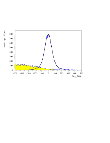
Cosmic ray data are taken regularly during breaks in the HERA machine operation. Penetrating tracks with 4 hits in the CST are selected. The parameters of the ’upper’ and the ’lower’ track must agree within errors, which leads to four constraint equations. As an example figure 8 shows the distribution of the difference of the track positions at their closest approach to the origin of the H1 coordinate system — the so-called muon miss-distance. After alignment the standard deviation of the Gaussian is 52 m, which corresponds to a single-track impact parameter resolution of 38 m for tracks with a transverse momentum above 4 GeV/c. The corresponding impact parameter resolution in the z-projection is 74 . Several million cosmic ray triggers are required for a sufficient illumination of all half-ladders.
6.2.2 Overlaps
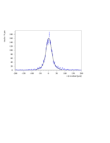
Cosmic tracks mainly constrain the relative positions of half-ladders in the inner and outer layer and in the upper and lower half of the CST. The position of neighbouring half-ladders are constrained by tracks passing through the overlap regions. Tracks with 3 hits are selected from normal luminosity data and are used to formulate two constraint equations, one in each readout coordinate. Two hits are used to define the track and to predict the hit in the overlap region. A distribution of residuals in the projection is shown in figure 9 from which an intrinsic point resolution of 12 m is inferred.
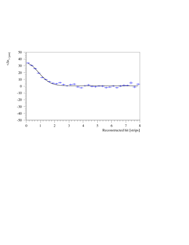
Close to the guard ring region of the sensors a systematic shift of the overlap residuals is observed. In figure 10 the mean of the residual distribution is shown as a function of the distance of the reconstructed cluster position from the guard ring. The shift is well described by a semi-Gaussian with an amplitude of 33 m and a width of 0.85 pitch units. The shift is attributed to charge collected on the guard ring. A correction is made and overlaps on the first two strips are not used in the alignment procedure.
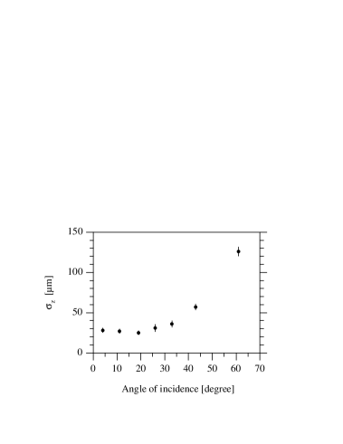
The angles of incidence do not deviate by more than 22o from the normal in the projection while much larger angles occur in the projection. The dependence of the intrinsic z-resolution (measured on the n-side) on the angle of incidence is shown in figure 11. It is well described by a parabola and reaches a minimum of 22 m at 15o from normal incidence [19].
6.2.3 Vertex Fits
Multi-track events from data are selected and a common 3D event vertex fit is performed. The sum of the values over several ten thousand events is included in the overall minimization with respect to the alignment parameters. This method alone does not lead to a robust estimation of the internal alignment parameters but together with cosmic rays and overlap tracks it provides a uniformly distributed track sample of high statistics that improves the quality of the combined alignment.
6.2.4 Alignment Procedure
The alignment is performed using the three data sets simultaneously. A common is accumulated and minimized iteratively with respect to the 384 local alignment parameters. The sparseness of the corresponding Hessian matrix is exploited for a fast solution of the linearized equations [21]. Two sets of alignment parameters were determined for 1997, using alignment data sets taken several months apart. The parameters are made comparable by applying six overall constraints, that correspond to a displacements or rotation of the entire CST. It is found that the internal alignment parameters agree with RMS spreads of 6 m and 0.1 mrad. Compared to the intrinsic silicon resolution this reproducibility and long-term stability is sufficient.
6.2.5 Global alignment
The global alignment determines the displacements and tilts of the entire CST with respect to the CJC and the z-chambers. Six parameters are determined by minimizing the differences between CST and CJC tracks, using events and cosmic rays.
7 Performance
7.1 Occupancy
The on-line zero-suppression on average finds 60 p-side clusters and 200 n-side clusters, corresponding to channel occupancies of 0.8% and 2%, respectively. The higher occupancy on the n-side is due to larger non-Gaussian tails in the noise distribution. The occupancies are stable in time. The average number of linked hits is 14 for each projection which represents the track-related occupancy.
7.2 Signal to Noise Ratio
Minimum ionizing particles have a most probable energy loss of 84 keV in 300 m of silicon, which leads to a signal of about 23 000 electron-hole pairs. The thermal noise level is determined by the preamplifier design, its operating conditions and the detector load capacitance. For three daisy-chained sensors the capacitance of one strip to all neighbours amounts to 27 pF on the p-side and 57 pF on the n-side, where the contribution from the double metallization dominates. The APC is routinely operated in a triple sampling mode and with a power dissipation of 0.3 mW per channel.
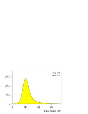
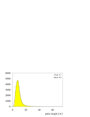
Figure 12 shows the distribution of cluster pulse heights divided by the average single-channel noise for cosmic muon tracks, normalized to vertical incidence. The shape is well described by a Landau energy loss distribution with a most probable signal-to-noise ratio of 19 for the p-side and 6.7 for the n-side, see figure 13. The difference is due to the strip capacitance loading the preamplifier which is a factor of two larger on the n-side, and due to the incomplete charge amplification caused by the limited gain of the preamplifier.
7.3 Efficiency
The CST hit efficiencies are most accurately determined with cosmic tracks passing through four CST half-ladders. Using three linked hits and the curvature from the CJC the track parameters are determined in a fit and the intersection with the fourth half-ladder is calculated. Figure 14 shows for a sample of 20000 muon tracks with transverse momentum above 2 GeV the distance between the intersection point and all hits in the test layer in the z-projection.

The central peak at zero contains the signal hits while the noise hits create a flat background distribution. The central peak can be described by two gaussians with widths of 33 m and 64 m for test half-ladders in the inner and outer layer, respectively. By comparing the number of hits in the peak with the number of passing tracks one can determine the hit-efficiencies. Fig. 15 shows the results for p- and n-side hits for all 64 half-ladders.

Besides some fluctuations, which can be associated with specific hardware problems for the selected data runs, the efficiencies are in agreement with being the same for all half-ladders. For the p-side the average efficiency is 97%, while it is 92% for the n-side. The inefficiencies is caused by silicon defects, dead or noisy readout channels, the hit finding algorithm and the linking procedure. The lower efficiency for n-side is due to the lower signal-to-noise ratio.
7.4 Beam Line Reconstruction

A precise knowledge of the beam position as a function of time is required for many decay-length or impact parameter studies. The beam position and tilt is determined by accumulating CST tracks over typically 30 minutes and minimizing the closest approach to a line in space. Figure 16 shows the horizontal and vertical beam position determined for the 1997 luminosity period. The horizontal beam movements reflect adjustments to the HERA optics.
The remaining distribution of the closest approach to the beam line () has a central Gaussian part with contributions from the CST intrinsic resolution, from multiple scattering in the beam pipe and the first silicon layer and from the beam spot size. The decays of long-lived particles contribute to the non-Gaussian tails. From the HERA machine optics an elliptical beam spot with a horizontal-to-vertical aspect ratio of 5 to 1 is expected. This allows to separate the different contributions by measuring the width of the central Gaussian of the distribution as a function of the track direction around the beam. The result is shown in figure 17 for tracks with high momentum where the multiple scattering contribution can be neglected.
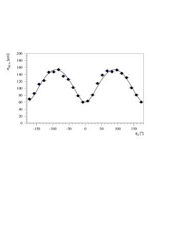
A fit of the form
is used to extract the CST intrinsic resolution of m and a horizontal beam spot size of m, which agrees with the HERA optics. A ratio as given by the optics was assumed in the fit to unfold the CST intrinsic resolution.
7.5 Impact Parameter Resolution

The multiple scattering contribution to the width of the can be measured as a function of momentum by unfolding the contribution of the beam spot size. This contribution is minimal for horizontal tracks. The result is shown in figure 18 for data from 1997 and from 1999. A fit according to
leads to asymptotic values of m and m for the two years while the parameter improves by a factor 1.55, as expected for the change from an aluminium beam pipe () to a carbon fiber beam pipe (), when adding the constant contribution of the first silicon layer and the CSt inner shield.
8 Summary
The H1 silicon vertex detector CST has been operated successfully at HERA since the beginning of 1997. The sensors, the readout electronics and the optical signal transmission are functioning reliably and efficienctly. A point resolution of 12 m with a signal-to-noise ratio of 19 has been achieved for the coordinate, while the minimal point resolution in is 22 m with a signal-to-noise ratio of 7. An impact parameter resolution of 37 m in the plane has been achieved for high momentum tracks, which opens a wide range of physics topics in the field of heavy quark production in electron-proton collisions.
References
- [1] I. Abt et al., Nucl. Instr. and Meth. A386 (1997) 310 and A386 (1997) 348
- [2] H1 Collaboration, Technical proposal to build silicon tracking detectors for H1, DESY PRC 92/01, July 1992; R. Horisberger, Proc. Int. Europhysics Conf. on High Energy Physics, Marseille, July 1993
- [3] R. Eichler and S. Frixione, Proceedings Future Physics at HERA, Hamburg 1996, G. Ingelmann, A. DeRoeck, R. Klanner (editors)
- [4] W. Eick et al., Nucl. Instr. and Meth. A386(1997) 81
- [5] M. Biddulph, PhD thesis No ETH-12331, (1997)
- [6] D. Pitzl et al., Nucl. Instr. and Meth. A348(1994) 454
- [7] Wacker Chemitronics, Burgdorf, Germany
- [8] C.S.E.M. SA, CH 2007 Neuchâtel, Maladière 71, Switzerland
- [9] Siltronix SA, CH-1214 Vernier Geneva, Switzerland
- [10] Radeberger Hybridelektronik GmbH, D-01454 Radeberg, Germany
- [11] W. Erdmann et al., Nucl. Instr. and Meth. A372(1996) 188
- [12] J. Buerger et al., Nucl. Instr. and Meth.A386(1997) 269
- [13] W.J. Haynes et al., Nucl. Instr. and Meth. A403(1998) 313
- [14] CES 8320 RIO2, Creative Electronic Systems, Geneva
- [15] A prototyp version with 12 channels has been described in: R. Horisberger and D. Pitzl, Nucl. Instr. and Meth. A326(1993) 92
- [16] Faselec AG, Philips Semiconductor, Binzstr. 44, CH-8045 Zürich, Switzerland.
- [17] G. Klaiber, Diplomathesis ETH-Zurich 1996, unpublished
- [18] Rohacell from Roehm AG, Switzerland
- [19] J. Gassner, Diplomathesis ETH-Zurich 1996, unpublished
- [20] L Jönsson, B. Lundberg, U. Mjörnmark, Lund University, Sweden
- [21] V. Blobel, private commuinication. See also http://www.desy.de/blobel/