High reflectivity grating waveguide coatings for 1064 nm
Abstract
We propose thin single-layer grating waveguide structures to be used as high-reflectivity, but low thermal noise, alternative to conventional coatings for gravitational wave detector test mass mirrors. Grating waveguide (GWG) coatings can show a reflectivity of up to 100% with an overall thickness of less than a wavelength. We theoretically investigate GWG coatings for 1064 nm based on tantala (Ta2O5) on a Silica substrate focussing on broad spectral response and low thickness.
pacs:
04.80.Nn, 42.79.Gn, 42.79.Dj1 Introduction
Dedicated research during the last few years has revealed that thermally driven motion of the test masses, so-called thermal noise [1] is larger than foreseen in future gravitational wave detectors. A major, but previously underestimated, contribution is given by the multilayer dielectric coating stacks of the high reflectivity test mass mirrors [2, 3]. This currently limits the design sensitivity of the Advanced LIGO detector [4]. In conventional schemes, up to 40 layers of Ta2O5 and SiO2 with an optical thickness of a quarter wavelength are needed to reach high reflectivities sufficiently close to 100%. The thermal noise of the coating is due to the mechanical loss of the layers with a dominant contribution from Ta2O5. New concepts are required that have less loss but still achieve the required high reflectivity. One approach being pursued is to design an alternative multilayer system deviating from the classical quarter wave design and containing less Ta2O5 [5]. Doping of Ta2O5 with TiO2 has also been investigated and a reduction of the loss by a factor of 1.5 was observed [6]. Another approach is to avoid high reflection coatings at all by the use of corner reflectors which employ total internal reflection instead of multiple interference at different layers to reach high reflectivity [7]. However, in this case thermo-refractive noise which results from a temperature dependent refractive index and also thermal lensing are increased due to the large optical path length in the substrate material.
Grating waveguide structures [8] provide another possibility to construct high reflectivity devices. The interest of earlier work on grating waveguides lay mainly in narrow-band (highly resonant) devices for applications in optical filtering [9] and optical switching [10]. However, grating waveguide structures can also provide broad-band (weakly resonant) reflectors. This turns them into interesting candidates for test mass coatings in gravitational wave detectors, because only a very small amount dielectric coating material is required with a corresponding considerable reduction in coating thermal noise.
2 Resonant grating waveguide structures

The remarkable property of a grating waveguide (GWG) is that it can show a reflectivity of 100 % for a given optical wavelength despite its thickness of typically less than a wavelength. For an extensive overview of grating waveguides we refer to Ref. [11]. In the simplest case a GWG consists of a substrate material with low refractive index followed by a waveguide layer with high refractive index which has periodic corrugation with period as shown in figure 1. A simplified ray picture [8] can be used to understand its behavior. The structure can be designed such that light incident onto the grating will only produce one diffraction order in reflection (0R) but three diffraction orders in transmission (0T and 1T). (For clarity the -1T order has been omitted in figure 1.)
The first order beams are coupled into a layer of high refractive material where they are stored due to total internal reflection. Light inside the waveguide is also coupled out via the grating. For a proper choice of grating parameters and incident angle the light coupled out from the layer (1R*) interferes destructively with the zero order transmitted beam (0T) and the device is a perfect reflector.
The possible parameter range for the period depends on the angle of incidence , the (vacuum) laser wavelength (), and the refractive indices and and can be calculated from the grating equation
| (1) |
where is the angle of the th diffraction order. For test mass mirrors in gravitational wave detector Michelson interferometers the angle of incidence is typically restricted to . To ensure that only the order is allowed in reflection,
| (2) |
has to hold. Another condition is that only orders in transmission exist from which follows that
| (3) |
Total internal reflection of the first order at the boundary of the waveguide and the substrate material is ensured if
| (4) |
A resonant grating waveguide structure has analogous behavior to a Fabry-Perot resonator: with decreasing coupling to the waveguide the finesse of the structure increases [8]. For high reflectors in GW detectors high finesse structures are disadvantageous, because small deviations from the design parameter would dramatically decrease the reflectivity for the desired wavelength . Additionally the power built up inside a high finesse waveguide could be a problem for high-power laser interferometers. Accordingly, a broadband resonance is desired for the high reflector.
3 Spectral response of waveguide coatings
Using rigorous coupled wave (RCW) analysis [12] it is possible to calculate the optical properties of the structure. Design considerations for binary gratings must include groove depth , waveguide thickness and ridge width , see figure 1, in addition to the before mentioned period and refractive indices and . The goal is to design a broad band reflection being less sensitive to fabrication tolerances and avoiding the problem of strong light power buildup in the waveguide. Here we restrict ourselves to and This corresponds to tantala and fused silica which are the favorite high index coating material and test mass material respectively [2].
According to (2) – (4) the following constraints apply to the period when one assumes the commonly uses Nd:YAG laser wavelength of nm:
| (5) |
For a broadband response, the coupling to the waveguide which corresponds to the diffraction efficiency of the 1T ray should be maximized. It only depends on the grating properties and but not on the thickness of the waveguiding layer. Figure 2 shows how the coupling depends on the groove depth and fill factor for selected values of for TM (magnetic field vector is parallel to the grooves) illumination.
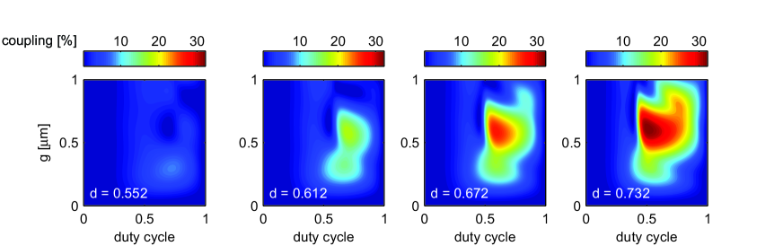
The plots indicate that the maximum coupling increases with increasing period . This is illustrated in figure 3 where we plotted the maximum values of the coupling obtained when and were varied according to figure 2 versus grating period for TM and TE polarization.
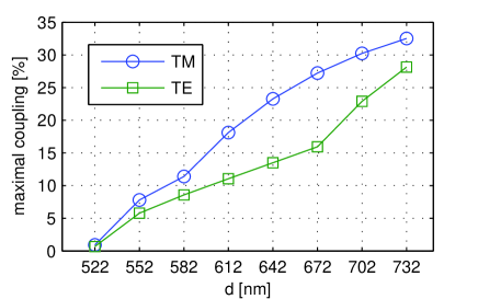
Hence for the purpose of a broad-band reflection peak large values for the grating period are favorable.
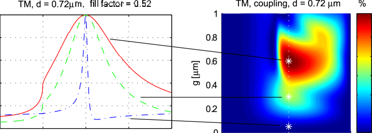
The direct connection between coupling and spectral width of the resonance is illustrated in figure 4. The right-hand side of the figure shows again the coupling to the waveguide versus groove depth and fill factor for a specific grating period. For three selected values of the groove depth (marked with three asterisks) and fixed fill factor, we determined the optimal waveguide thickness for a resonance peak around nm. On the left hand side of figure 4 we show the reflectivity versus the deviation from for the corresponding waveguide coating.
4 Thickness of the coating
The crucial factor for coating thermal noise in gravitational wave detector test masses is the overall thickness of the high index coating material. To reach a reflectivity of ppm with a stack of SiO2 and Ta2O5, typically 40 layers are needed, adding up to m overall tantala thickness. In contrast to this, a grating waveguide mirror can get along with a tantala thickness of much less than a wavelength.
In addition, if the total thickness of tantala in the waveguide structure is to be compared with a conventional mirror, one has to take into account that the grating region is not uniformly filled. Hence to first order approximation one can assume that the coating thermal noise should be proportional to an effective tantala thickness of .
The layer thickness determines the phase of the light travelling in the waveguide and hence the resonance condition of the device. The thickness for which a resonance occurs varies if the grating parameters and are changed as illustrated exemplary in figure 5, where the power reflectivity is plotted versus the groove depth and the waveguide thickness.
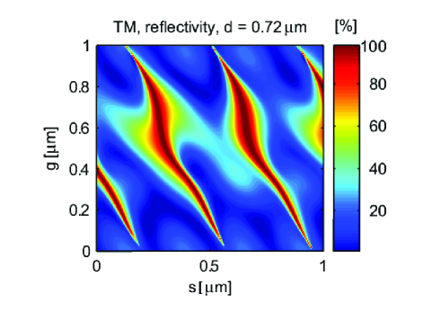
One can see a periodic behavior of the reflectivity as varies as expected. More interesting to note is that for a certain value of the 100 % reflectivity resonance occurs at . Accordingly the grating itself can provide perfect reflection and no waveguide layer is needed. This is extremely useful since the amount of the high index material can be greatly reduced.
An optimal design of a grating waveguide coating for gravitational wave detectors will be a tradeoff between the broadest spectral response and the smallest effective tantala thickness. As an example we consider the GWS corresponding to the dashed (green) curve on the left hand side of figure 4 which still has nm. With m and m the effective tantala thickness is only about m. This suggests a thermal noise reduction by more than an order of magnitude compared to a conventional coating.
5 Parameter tolerances
When designing diffractive structures one also has to consider how accurately grating parameters and layer thicknesses can be manufactured by state of the art procedures and how strongly deviations from design values affect the performance of the waveguide coating. Here we consider the fabrication errors in the waveguide thickness and how they can be compensated by tuning the laser wavelength. figure 6 shows how the power reflectivity of a waveguide is affected when the thickness of the waveguide or the wavelength of the laser deviate from their optimal values and respectively.
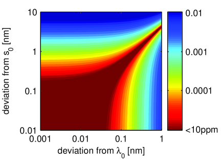
A typical power reflectivity requirement for GW detectors is ppm. Typical production accuracies of thin films are on the order of 1nm. The deviation from could be compensated by tuning the laser wavelength a small fraction of a nanometer. Deviations in other grating parameters affect the reflectivity by a similar way.
6 Conclusion
We have proposed a high reflectivity grating waveguide coating for advanced gravitational wave detectors which can provide perfect reflection despite the small amount of coating material that is needed. This has great potential to lower the coating thermal noise of high reflectivity mirrors. Focussing on a laser wavelength of nm and tantala as the coating material we presented sample calculations of the spectral response of the coating as well as the overall tantala thickness of the coating. Our analysis was based on RCW analysis and assumed plane wave inputs as well as infinite gratings. Future theoretical work will include gaussian input beams and finite grating size effects. On top of that more sophisticated designs of grating waveguide structures like double periodic structures [15] or double gratings [16] will also be investigated. Future experimental work will aim for a detailled characterization of such devices as an alternative to conventional high reflectivity multilayer dielectric coating stacks. An important issue will be the reduction of optical losses that may arise from writing errors during grating fabrication.
References
References
- [1] Braginsky V B et al 1999 Phys. Lett. A 264 1–10
- [2] Harry G M et al 2002 Class. Quantum Grav. 19 897–917
- [3] Fejer M M et al 2004 Phys. Rev. D 70 082003
- [4] www.ligo.caltech.edu/advLIGO
- [5] Agresti J at al [paper currently in LSC review]
- [6] Harry G M et al 2006 Appl. Opt. 45 1569–74
- [7] Braginsky V B et al 2004 Phys. Lett. A 324 345–60
- [8] Sharon A et al 1997 J. Opt. Soc. Am. A 14 2985–93
- [9] Sharon A et al 1996 Appl. Phys. Lett 69 4154–6
- [10] Sharon A et al 1996 Opt. Lett. 21 1564-6
- [11] Rosenblatt D et al 1997 IEEE J. Quantum Electron. 33 2038–59
- [12] Moharam M G et al 1982 J. Opt. Soc. Am. 72, 1385–92
- [13] Mateus C F R et al 2004 IEEE Photon. Technol. Lett. 16 518–20
- [14] Mateus C F R et al 2004 IEEE Photon. Technol. Lett. 16 1676–8
- [15] Lemarchand F et al 1998 Opt. Lett. 23 1149–51
- [16] Kappel C et al 2004 J. Opt. Soc. Am. B 21 1127–36