A simple model for the metal-insulator transition in a two-dimensional electron gas
Abstract
We introduce an elementary model for the electrostatic self-consistent potential in a two-dimensional electron gas. By considering the perpendicular degree of freedom arising from the electron tunneling out of the system plane, we predict a threshold carrier density above which this effect is relevant. The predicted value agrees remarkably well with the onset for the insulator to quasi-metallic transition recently observed in several experiments in SiO2–Si and AlGaAs–GaAs heterojunctions.
pacs:
PACS number(s): 36.20.Kd; 78.30.LyAnderson transition [3] in disordered solids still raises great interest among researchers. While metal-insulator transition (MIT) is well established in three-dimensional (3D) disordered systems, the situation is not completely understood in one- (1D) and two-dimensions (2D). Several decades ago, a number of papers yields the general belief that in those systems all eigenstates are exponentially localized and a MIT no longer exists[4, 5, 6]. Although this seems to be correct in most low-dimensional systems, there exist known exceptions to this rule. Thus, it has been found that extended states may appear in 1D random systems upon introducing either short-range [7, 8, 9, 10, 11, 12] or long-range [13, 14] correlations in the disorder. These purely theoretical considerations were put forward for the explanation of high conductivity of doped polyaniline [10] as well as transport properties of random semiconductor superlattices [15].
The Anderson transition induced by diagonal disorder at the band center in finite 2D systems was already studied by Yoshino and Okazaki [16]. The relevance of these midgap states for the metallic conductance of 2D systems has been discussed in detail by Licciardello and Thouless [17]. These authors suggested that between the mobility edges there is a tendency for the conductance to decrease slowly as the sample size is increased and that they may be no absolute minimum metallic conductance. However, recent experiments have provided clear evidences of the MIT-like in high-quality 2D electron and hole systems. After the pioneering work by Kravchenko et al. on electrons in Si [18, 19, 20] and more recently by Hanein et al. on holes in GaAs [21], it has be become clear that 2D gases undergo a crossover from an insulating regime at low density to a metalliclike behavior at high density, where the quasi-metallic phase is characterized by a strong decrease of the resistivity as the temperature decreases. Discrepancies between the standard one-parameter scaling theory [5], establishing that the 2D gas should be insulating, and the above mentioned experiments are usually attributed to a strong electron-electron interaction. A number of theoretical models have then been proposed to explain the observed transition in 2D systems, ranging from new liquid phases [22], Wigner glass [23], spin-orbit induced transition [24], decoherence due to quantum fluctuations [25], superconducting phase [26] and anyon superconducting model [27]. The basic ingredient of these models is the assumption that the system is purely 2D and, consequently, new phenomena are to be considered to explain the observed transition. In this work we undertake a different way by considering the electronic motion in the perpendicular direction. In so doing, we find the conditions under which this degree of freedom could be relevant. Surprisingly, the critical carrier density leading to perpendicular motion is close to that determined in experiments to observe the transition. Our main aim is then to point out the importance of this perpendicular degree of freedom, which should be taken into account in more elaborated models.
Our approach is based on the competition between the confining potential, appearing at the heterojunction even at zero gate voltage, and the repulsive potential arising from the excess carrier at nonzero gate voltage. To proceed, let us start by considering the heterojunction at zero gate voltage. Since we are only interested in the basic phenomena without entering in many details, we make use of a simple variational Hartree calculation presented in standard textbooks [28]. This will make our reasonings clearer while keeping a good qualitative description of the involved physics. The envelope function of the lowest subband of a 2D electron gas is reasonably well accounted for by the Fang-Howard trial function:
| (1) |
where is the coordinate along the growth direction (perpendicular to the heterojunction) and is determined by minimizing the kinetic energy plus the Hartree energy per electron (see Ref. [28] for details). In terms of the effective Bohr radius, , and the 2D electron density, , the variational parameter is roughly given by
| (2) |
while the maximum value of the Hartree potential is [28]
| (3) |
being the dielectric constant of the medium. The Hartree potential increases smoothly from zero up to on increasing the distance from the heterojunction. Thus, at zero gate voltage the electrons lie on the lower subband and confined, thus forming a 2D gas. The lower subband energy is expressed as:
| (4) |
The situation may be different when the gate voltage induces an excess carrier density , as we will show below. This excess carrier is not compensated by any other charge close to the heterojunction, thus leading to a local negative charge density. As a crude and first approximation, we assume that this excess charge density is confined to a plane close to the heterojunction. By solving the Poisson equation, one can obtain the potential energy due to this charged plane, namely for , where
| (5) |
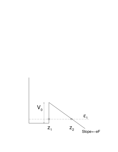
Due to this repulsive potential, electrons may tunnel through the barrier formed by the Hartree potential plus and escape. To account for the tunneling process, we replace the actual potential by that depicted in Fig. 1. This replacement is not essential in the calculations since both the confining Hartree potential and the repulsive potential due to the charged plane are known, but it allows us to obtain closed analytical expressions for the transmission coefficient. Since the Fermi energy is usually very small in this system, we can also safely neglect it when calculating the transmission coefficient and take , as indicated in Fig. 1. Thus, the classical turning points are and , shown in the figure. From the WKB semi-classical approximation, the transmission coefficient is given by
| (6) | |||||
| (7) |
The onset for the crossover from a 2D to 3D behavior can be determined from the condition that the transmission probability is large. We then assume that this crossover appears when the exponent in (7) is of the order of unity in absolute value. This occurs for a critical density such that
| (8) |
Since is a function of , we can readily determine the value of the critical density from the above condition for which the probability for tunneling out of the well is large. Using (3), (4) and (5) we finally obtain . Since the carrier density at zero gate voltage is related to the Fermi energy by the expression , we finally arrive at the condition
| (9) |
where the Fermi energy is measured in meV and the effective mass in units of the free electron mass.
Now let us compare our qualitative prediction (9) with the experimental values. A 2D electron gas in Si has been studied by Kravchenko et al. [20], who observed the transition for an electron density cm-2. The Fermi energy was meV and the effective mass . Inserting both values in (9) we obtain a critical density cm-2. On the other side, 2D hole gas in GaAs was demonstrated to undergo a MIT at a hole density cm-2 by Hanein et al. [21]. Taking the values meV and we get from (9) that cm-2. The agreement should be regarded as surprisingly good, in view of the crude approximation we made to obtain it. As a conclusion, our model points out the relevance, under some circumstances, of the perpendicular degrees of freedom in the so-called 2D electron gases. As soon as the electron gas becomes a non-perfect 2D system, the scaling theories predicts the occurrence of a MIT transition like that recently observed.
The authors warmly thank I. Gómez for his useful comments and criticisms, and E. Diez, C. Kanyinda-Malu and M. Hilke for helpful conversations. FDA was supported by CAM under Project 07N/0034/98. JCF was supported by CICOPS fellowship of University of Pavia.
REFERENCES
- [1] Permanent address: Universidad de Tarapacá, Departamento de Física, Casilla 7-D, Arica, Chile.
- [2] Permanent address: GISC, Departamento de Física de Materiales, Universidad Complutense, E-28040 Madrid, Spain.
- [3] P. W. Anderson, Phys. Rev. 109, 1492 (1958).
- [4] N. F. Mott and W. D. Twose, Adv. Phys. 10, 107 (1961).
- [5] E. Abrahams, P. W. Anderson, D. C. Licciardello, and V. Ramakrishnan, Phys. Rev. Lett. 42, 673 (1979).
- [6] P. A. Lee and T. V. Ramakrishnan, Rev. Mod. Phys. 57, 287 (1985).
- [7] J. C. Flores, J. Phys.: Condens. Matter 1, 8471 (1989).
- [8] D. H. Dunlap, H.-L. Wu, and P. Phillips, Phys. Rev. Lett. 65, 88 (1990).
- [9] H.-L. Wu and P. Phillips, Phys. Rev. Lett. 66, 1366 (1991).
- [10] P. Phillips and H.-L. Wu, Science 252, 1805 (1991).
- [11] J. C. Flores and M. Hilke, J. Phys. A 26, L1255 (1993).
- [12] A. Sánchez, E. Maciá, and F. Domínguez-Adame, Phys. Rev. B 49, 147 (1994).
- [13] F. A. B. F. de Moura and M. L. Lyra, Phys. Rev. Lett. 81, 3735 (1998).
- [14] F. M. Izrailev and A. A. Krokhin, Phys. Rev. Lett. 82, 4062 (1999).
- [15] V. Bellani, E. Diez, R. Hey, L. Toni, L. Tarricone, G. B. Parravicini, F. Domínguez-Adame, and R. Gómez-Alcalá, Phys. Rev. Lett. 82, 2159 (1999).
- [16] S. Yoshino and M. Okazaki, J. Phys. Soc. Jpn. 43, 415 (1977).
- [17] D. C. Licciardello and D. J. Thouless, J. Phys. C 11, 925 (1978).
- [18] S. V. Kravchenko, G. V. Kravchenko, J. E. Furneaux, V. M. Pudalov, and M. D’Iorio, Phys. Rev. B 50, 8039 (1994).
- [19] S. V. Kravchenko, W. E. Mason, G. E. Bowker, J. E. Furneaux, V. M. Pudalov, and M. D’Iorio, Phys. Rev. B 51, 7038 (1994).
- [20] S. V. Kravchenko, D. Simonian, M. P. Sarachik, W. E. Mason, and J. E. Furneaux, Phys. Rev. Lett. 77, 4938 (1996).
- [21] Y. Hanein, U. Meirav, D. Shahar, C. C. Li, D. C. Tsui, and H. Shtrikman, Phys. Rev. Lett. 80, 1288 (1998).
- [22] S. He and X. C. Xie, Phys. Rev. Lett. 80, 3324 (1998).
- [23] S. Chakravarty, S. Kivelson, C. Nayak, and K. Volker, cond-mat/9805383.
- [24] V. M. Pudalov, cond-mat/9707076.
- [25] P. Mohanty, cond-mat/9912263.
- [26] P. Phillips and Y. Wang, cond-mat/9704200.
- [27] F. C. Zhang and T. M. Rice, cond-mat/9708050.
- [28] J. H. Davies, The Physics of Low-Dimensional Semiconductors, (Cambridge University Press, UK, 1998).