Broken symmetry of row switching in 2D Josephson junction arrays
Abstract
We present an experimental and theoretical study of row switching in two-dimensional Josephson junction arrays. We have observed novel dynamic states with peculiar percolative patterns of the voltage drop inside the arrays. These states were directly visualized using laser scanning microscopy and manifested by fine branching in the current-voltage characteristics of the arrays. Numerical simulations show that such percolative patterns have an intrinsic origin and occur independently of positional disorder. We argue that the appearance of these dynamic states is due to the presence of various metastable superconducting states in arrays.
pacs:
74.50.+r, 74.80.-g, 47.54.+rSpatiotemporal pattern formation in a system of nonlinear oscillators is governed by mutual coupling. Examples of such patterns are domain walls and kinks in arrays of coupled pendula, topological spin and charge excitations in large molecules and solids, and inhomogeneous states in many other complex systems[3]. A single driven and damped nonlinear oscillator displays two distinctly different states, a static state and a whirling (dynamic) state. Therefore, a system of coupled oscillators can show various spatiotemporal patterns with concurrently present static and dynamic states.
Arrays of Josephson junctions have attracted a lot of interest because they serve as well-controlled laboratory objects to study such fundamental problems as above mentioned pattern formation, chaos, and phase locking. In the systems of coupled Josephson junctions [4, 5, 6, 7, 8, 9, 10] the two local states are the superconducting (static) state and the resistive (dynamic) state. For underdamped junctions, these states manifest themselves by various branches on the current-voltage (-) characteristics. The hysteretic switching between branches has been found in stacks of Josephson tunnel junctions [6], layered high-temperature superconductors [7] and two-dimensional (2D) Josephson junction arrays [4, 5, 9, 10].
In 2D arrays, this switching effect appears in the form of row switching when a voltage drop in array occurs on individual rows of junctions perpendicular to the direction of the bias current. A typical behavior found in both experiments [9] and in numerical simulations [5, 11] is that the number of rows switched to resistive state and, even more important, their distribution inside the array can change during sweeping the - curve. An analysis of such row switching has been carried out recently [10] to predict the range of stability of the various resistive states. However, until now only relatively simple resistive states have been found. These states correspond to a whirling state of vertical junctions (placed in the direction of the bias current) and small oscillations of the Josephson phase difference of horizontal junctions (transverse to the bias) around their equilibrium state [10].
In this Letter, we report on the observation of new dynamic states with peculiar percolative patterns of the voltage drop inside homogeneously biased arrays. We have found broken symmetry in row switching such that the dc voltage drop meanders between rows. These states appear in dc measurements in the form of fine branching on the - curves. The states have been visualized by using the Low Temperature Scanning Laser Microscopy (LTSLM)[12]. We have also carried out numerical simulations in which similar dynamic states are found. The measured two-dimensional arrays consist of underdamped NbAl-AlONb Josephson junctions[13]. The junctions are placed at crossing of the superconducting striplines, that are arranged in either square lattice (with 4 junctions per elementary cell) or triangular lattice (with 3 junctions per elementary cell). An optical image of a 2D square array and the equivalent electrical circuit are shown in Fig. 1.
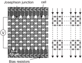
The junction area is 9 m2 and their critical current density is about KA/cm2 for square array, and KA/cm2 for triangular array, with a typical spread of junction parameters of about 5%. The square arrays consist of 10 columns by 10 rows and have the cell area m2. The triangular arrays are made of 12 columns by 12 rows and have m2. All arrays are underdamped and typical values of the McCumber parameter[14] at K are around 200. The parameter characterizing the influence of self-inductance [8, 10] changes from for triangular arrays to for square arrays.
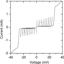
The bias current is injected uniformly via external resistors. The voltage is read in the direction along the bias, both across the whole array and across several individual rows. The - curves are digitally stored while sweeping the bias current occurs. The - characteristic of the square array is shown in Fig. 2. For every bias polarity, the number of branches is equal to the number of rows which are at the gap voltage state mV, and the highest gap voltage corresponds to the sum of gap voltages of the 10 rows. By choosing a bias point at a certain gap voltage, we can select the number of rows which will be in the resistive state, while the other rows remain in the superconducting state.
On the hysteretic part of the - curves, we have systematically observed a fine branching around the row gap voltages (Fig. 3(a)). The branching has been detected simply by recording a large number of - curves in the absence of externally applied magnetic field and at a constant sweep frequency and temperature (K). It was always possible to choose a stable dc bias point on a particular branch. The fine branching of the - curves around the gap voltages was found to be a typical feature of all studied arrays.
In order to determine the actual distribution of resistive paths in the array, we used the method of LTSLM [12]. The LTSLM uses a focused laser beam for local heating of the sample. The local heating leads to an additional dissipation in the area of several micrometers in diameter. The laser beam induced variation of the voltage drop across the whole sample is recorded versus the beam coordinates. This method allows to visualize the junctions that are in the resistive state. In order to increase the sensitivity and spatial resolution, the intensity of the beam is modulated at a frequency of a several KHz and the voltage response of the array is detected phase sensitively by lock-in technique.
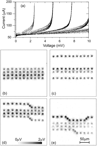
By using the LTSLM, we have systematically imaged different resistive configurations biased at various fine resistive branches of the - curves. The experimental procedure is the following: the number of switched rows is fixed by biasing the array at voltages . Then LTSLM images of the sample are recorded at a constant bias value. Typical images from the square array are shown in Fig. 3(b)-(e). The black spots correspond to the junctions that are in the resistive state. The junctions that are in the superconducting state do not appear on the array image. As expected, the images show that the number of rows which are in the resistive state is equal to the number of gap voltages selected by the bias point. To trap a different resistive configuration, we always increased the bias current above , the array critical current, and then reduced it to the low level.
Similarly to the experimental results of Ref. [9], we have found that most of the images show various combinations of straight resistive and superconducting rows (Fig. 3(b),(c)). However, the most striking feature of our measurements is that the resistive lines are not always straight, but may undergo a meandering towards the neighboring row involving one of the horizontal junctions in the resistive state, see Fig. 3(d).
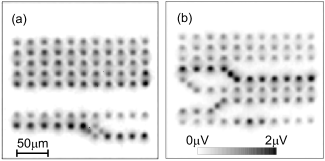
We have found that such a broken symmetry of row switching systematically appears in all studied arrays. Moreover, we have observed that the horizontal junctions switched to the resistive state were distributed randomly inside the array and have found no tendency for the meanders to occur at the same places. Thus, we suppose that the meandering is not predominantly due to any disorder in the junction parameters. The meandering of resistive paths is a rare event and its probability does not exceeds per horizontal junction of single switched row. Therefore, the observation of deviation of resistive paths from the straight lines is easier for larger arrays. We have also observed rare resistive states with two switched horizontal junctions in one row, as shows Fig. 3(e). Sometimes even more complicated distributions of switched junctions were registered [Fig. 4[(a),(b)].
In the following, we present numerical simulations of the dynamics of underdamped arrays. Calculations were performed using the resistively shunted model for Josephson junctions and the usual analysis for superconductive loops with only self-inductances taken into account, i.e. the Nakajima-Sawada equations [15]. For a discussion of these equations and the application limits see Refs. [8, 10]. The phase configuration of a row switched state was used as initial condition for the next run.
We simulated large () and small () square arrays with various parameter between 0.5 and 2. In all cases, the simulations well reproduce the branching of - curves and meandering character of the finite voltage paths. Moreover, in order to check the influence of self-inductance effects the simulation were carried out for the arrays with a small parameter . A simulated - curve with three different branches and the corresponding voltage distributions for the array are shown in Fig. 5. Resistive states with both single and double meanders have been trapped (Fig. 5). The appearance of the meandering is qualitatively similar to the experimental images shown in Fig. 3(b-e). The simulations have been carried out in the presence of finite magnetic field in order to prevent the simultaneous switching of all the array rows [10]. It leads to the decrease of the critical current and the appearance of the flux-flow region where - curves are highly non linear (Fig. 5).
We have found that, in the absence of disorder, the probability of the appearance of a meander in two row array is about per horizontal junction. Surprisingly, in the presence of specially introduced disorder up to the numerical simulations show no increase of the rate of appearance and no preferred position of the meanders. Due to this fact, we conclude that the broken symmetry row switching appears due to an intrinsic instability
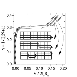
of the superconducting state, i.e. a change of the initial conditions can lead to the appearance of a different percolative voltage path. The numerical analysis of the two row array also allows to find out some peculiarities of the new dynamic states. When the junctions switched to the resistive state form a straight line in the top or bottom row (no meandering), the array has the highest resistance, (triangle symbols in Fig. 5), where is the total number of cells in the row and is the normal resistance of one junction. In the case when the voltage path with one meandering occurs, the array shows a lower resistance, (square, Fig. 5). Now there is one more junction connected in parallel to the resistive path, with respect to the case of no meandering. For the same reason, the meanders across two horizontal junctions corresponds, to the resistance (circle, Fig. 5). The presence of meanders shifts the array - curve to the left and this resistance scaling explains the experimentally observed fine branching of the - curves.
We have found that the above dynamic states are stable in a wide range of voltages, i.e. we have not observed direct switching between branches. This is due to the too large energy necessary for the junction capacitance recharge in underdamped arrays [14]. So, only switching from the superconducting state allows to trap these dynamic states.
Our analysis using the Kirchhoff’s current laws shows that, in the case of meandering, the dc superconducting current flows via the horizontal junctions. Moreover, this current increases from the row boundary to the cell where the meandering occurs. This current configuration is different from that without meanders. In the latter case the horizontal junctions are not active and dc superconducting current flows only via the vertical junctions.
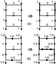
All these features can be explained, at least qualitatively, by the presence of metastable superconducting states in 2D Josephson arrays. We analyze these states for a simple case of two plaquettes with 5 junctions (Fig. 6). In the absence of magnetic field, the most stable superconducting state is the one with all mesh currents equal zero. At the bias current the vertical junctions switch from superconducting state to resistive state with straight resistive rows (dc mesh currents are still zero) (Fig. 6(a)). However, this system has another peculiar state with finite values of mesh currents, as shown in Fig. 6(b). At this system can support a superconducting state with the Josephson phases of the horizontal junction and one vertical junction per row being equal to . The Josephson phases of the remaining vertical junctions are equal to . This metastable state supports finite mesh currents and switches to the dynamic (resistive) state with a meander via the horizontal junction. The mesh currents decrease to the value of and change sign during the switching process, which results in a stable dynamic state with meandering. Thus, the dynamic states with meandered dc voltage drop are ”fingerprints” of metastable superconducting states with non zero mesh currents and active horizontal junctions. The state appears only when there are at least three junctions per cell and it exists also in the limit of zero linear self-inductance and zero magnetic field [16]. That is different from the case of single- and double-junction SQUIDs, where metastable superconducting states appear only in the limit of large self-inductance [14]. Since the above discussed metastable state exists in the limit of zero inductance, the small arrays with few plaquettes can be suitable system to observe the effect of macroscopic quantum coherence at low temperatures[14, 17].
It appears that also large 2D arrays can provide various metastable superconducting states that lead to the broken symmetry in row switching process. Theoretical and experimental investigation of these metastable superconducting states and their dependence on the externally applied magnetic field are in progress.
This work was partially supported by the European Office of Aerospace Research and Development (EOARD), the Alexander von Humboldt Stiftung, the German-Israeli Foundation, and the German-Italian DAAD/Vigoni exchange program.
REFERENCES
- [1] Unitá INFM Salerno and Science Faculty, University of Sannio Via Port’Arsa 11, 82100 Benevento, Italy
- [2] OXXEL GmbH, Technologiepark Universität, Fahrenheitstrasse 9, D-28359 Bremen, Germany
- [3] S.H. Strogatz, Nonlinear Dynamics and Chaos: With Applications to Physics, Biology, Chemistry, and Engineering, Addison-Wesley, Reading, MA (1994).
- [4] H.S.J. van der Zant, C.J. Müller, L.J. Geerlings, C.J.P.M. Harmans, and J.E. Mooij, Phys. Rev. B38, 5154 (1988).
- [5] W. Yu, K.H. Lee, and D. Stroud, Phys. Rev. B47, 5906 (1993).
- [6] N. Thyssen, A. V. Ustinov, and H. Kohlstedt, J. Low.Temp. Phys. 106, 201 (1997).
- [7] R. Kleiner and P. Müller, Phys. Rev. B49, 1327 (1994).
- [8] G. Filatrella and K. Wiesenfeld, J. Appl. Phys. 78, 1878 (1995).
- [9] S.G. Lachenmann, T. Doderer, D. Hoffmann, R.P. Hübener, P.A.A. Booi, and S.P. Benz, Phys. Rev. B50, 3158 (1994).
- [10] M. Barahona and S. Watanabe, Phys. Rev. B57, 10893 (1998).
- [11] J. R. Phillips, H.S.J. van der Zant, and T. P. Orlando, Phys. Rev. B50, 9380 (1994).
- [12] A. G. Sivakov, A. P. Zhuravel’, O. G. Turutanov, and I. M. Dmitrenko, Appl. Surf. Sci, 106, 390, (1996).
- [13] HYPRES Inc., Elmsford, NY 10523.
- [14] K. K. Likharev, Dynamics of Josephson junctions and circuits, Gordon and Breach, New York, 1981.
- [15] K. Nakajima and Y. Sawada, J. Appl. Phys. 52, 5732 (1981).
- [16] A similar state can be found in a single anisotropic plaquette with three junctions per cell when the parameter of anisotropy (M. V. Fistul, to be published). Here, and are, respectively, the critical currents of the horizontal and vertical junctions.
- [17] J. E. Moiij, T. P. Orlando, L. Levitov, L. Tian, C. H. van der Wal, and S. Lloyd, Science 285 , 1036 (1999).