Bandgap renormalization of modulation doped quantum wires
Abstract
We measure the photoluminescence (PL) spectra for an array of modulation doped, T-shaped quantum wires as a function of the 1d density which is modulated with a surface gate. We present self-consistent electronic structure calculations for this device which show a bandgap renormalization which, when corrected for excitonic energy and its screening, are largely insensitive to and which are in quantitatively excellent agreement with the data. The calculations show that electron and hole remain bound up to and that therefore the stability of the exciton far exceeds the conservative Mott criterion.
Exchange and correlation in an electron gas formed in a semiconductor act to counter the direct Coulomb interaction by reducing the inter-particle overlap. For two component systems, such as the electron-hole plasma created in optical experiments, this effect tends to produce a bandgap renormalization (BGR) with increasing density and/or , which reduces the energy of photons emitted upon recombination from the band edges [1]. Exciton formation further reduces the bandgap but exciton binding is weakened by mobile charges and so the trend with density opposes that of exchange-correlation induced BGR. Investigations of the bandgap, which has a pivotal dependence on the dimensionality of the system, is of interest both for its significance to optical technology and for the illumination it provides for the many-body problem. Consequently there are numerous experimental and theoretical studies of BGR which have focused on systems of successively lower dimension over the past several years [2, 3].
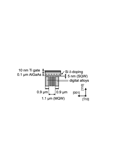
For one dimensional systems, or quantum wires (QWRs), a number of recent experimental and theoretical accounts have begun to clarify the often competing effects which result in density dependent changes to the observed photoluminescence energy [4, 5, 6, 7, 8, 9]. In general, BGR depends on the densities, and , of both components of the electron-hole plasma. Typically, however, research has concentrated on intrinsic samples wherein . One difficulty with this approach has been that in order to vary , an increase in photoexcitation has been required, or else the time development as the excitation subsides has been observed, and the resulting spectra are complicated with highly non-equilibrium effects such as phase space filling. In this paper we present an experimental study of the evolution of the photoluminescence energy in a doped, T-shaped QWR sample whose conduction band electron density can be modulated with the voltage applied to a surface gate. This structure (see Fig. 1), fabricated via the cleaved edge overgrowth techniques [10] has appreciable advantages. First it provides wires of high precision, with structural variations restricted to the monolayer regime. Second, it permits the comparison of wire and quantum well photoluminescence in a single sample.
To complement the measurements, we perform self-consistent electronic structure calculations within density functional theory (DFT) for this structure, using the local density approximation (LDA) for exchange and correlation (XC), . The theoretical bandgap renormalization, which is usually calculated with many-body techniques, is equivalent to the difference between the LDA calculated bandgap and that calculated within a pure Hartree approximation, which omits the term. We have further calculated the effect of exciton formation and its screening on the bandgap, using a simplified model potential with parameters derived from the (translationally invariant) DFT calculation.
Our principle result is that, as with experiments on two-component plasma in V-groove wires [5], the photoluminescence peak position is largely insensitive to density. The calculated screening of the exciton reduces the binding energy with a functional form that neatly cancels most of the XC induced BGR, predicting a recombination energy in excellent agreement with experiment. Additionally, the appearance of sharp structure in the PL data, indicating recombination from excitons localized at monolayer potential fluctuations, which gradually vanishes with increasing , supports this BGR+exciton screening model. The calculation suggests that the exciton remains bound for very high density, also in agreement with Ref. [5], however the sharp structure disappears at much lower density, , indicating delocalization of the exciton.
The cleaved edge overgrowth (CEO) technique employed for our QWR structure has been described in detail elsewhere [10]. Our structure consists of 22 periods of (001)-oriented () / () quantum wells (multiple quantum wells, MQWs), grown between two digital alloys with 90 periods of () / () each. These digital alloys permit us to observe the PL from the overgrowth single quantum well (SQW), which is defined by growing along the [110]-crystal axis , a spacer, a silicon -doping (n-modulation doping), and . After both growth steps, 10 nm thick cap layers are added, which are not included in Fig. 1.
T-shaped QWRs form with atomic precision at each wide intersection of the SQW with one of the multiple quantum wells [11, 12].
In order to continuously vary the electron density in the QWRs and the SQW, we evaporate a thick, semi-transparent titanium gate on the surface of the overgrowth layer of a second set of samples. When the gate is grounded, the electron density in the SQW and in the QWRs are close to that of the un-gated samples.
To maximize spatial resolution of the photoluminescence (PL) and photoluminescence excitation (PLE) spectroscopy, we focus the excitation beam of a tunable cw dye laser, pumped by an -ion laser, with a microscope objective onto the sample, which is attached inside a cryostat to a copper block at the nominal temperature . On the sample, the diameter of the almost diffraction-limited laser spot amounts to about full-width at half-maximum. A confocal imaging system guarantees that only PL limited to the laser spot region is detected.
For both un-gated and gated samples, PLE spectra reveal that, due to an electron transfer from the doping layer into the SQW, an electron system is generated both in the SQW, between digital alloy and overgrowth spacer, and in the QWRs.
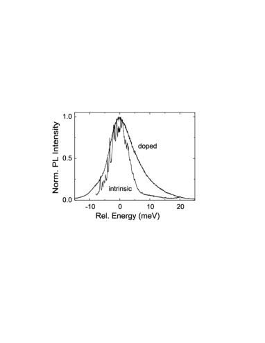
Exciting an un-gated sample on the ()-surface, we are able to identify the QWRs PL because it is localized exactly and exclusively at the intersecting region of single and multiple quantum wells and is emitted at lower energy than the PL of the SQW and the MQWs [13]. Of course, individual QWRs cannot be resolved, since they are spaced by only, with respect to a spatial resolution of our instrument of about . In order to interpret the PL lineshape of the n-modulation doped T-shaped QWRs, we compare it with the lineshape of intrinsic T-shaped QWRs, as shown in figure 2 (the curves are aligned horizontally so that the peaks coincide). Interface roughness, particularly in the (110)-oriented single quantum well [14], results in an inhomogeneously broadened, on average symmetric PL line of the intrinsic QWRs. The spectrally sharp peaks on the PL line are attributed to excitons localized at monolayer potential fluctuations [15]. In the presence of free carriers, however, the excitonic electron-hole interaction is screened [16] and the sharp peaks on the PL line disappear in the case of n-modulation doped QWRs. Furthermore, the asymmetric PL lineshape indicates the formation of an 1D electron plasma in our modulation doped QWRs and, as the dominating recombination mechanism, band-to-band transitions between electrons of the Fermi sea and photogenerated holes. The Maxwell-Boltzmann distribution of the photogenerated holes and the joint one-dimensional density of states [6] result in a decreasing recombination rate with increasing transition energy, if we assume a constant transition matrix element for k-conserving band-to- band recombinations [6]. In k-space, these transitions occur from the -point of the first Brillouin zone up to the Fermi wave vector, if we presume low temperatures. The decrease of the recombination rate with increasing transition energy is interpreted as the origin of the wide high energy tail and therefore the asymmetry of the PL line for the modulation doped QWRs. On the other hand, observing band-to-band transitions means that the electron density in the QWRs, whose charge density is estimated at [17], exceeds the Mott density [16]. According to simulation results [17], only electrons in the first QWRs subband have maximum probability density at the T-intersections. Electrons in the second subband are localized principally between pairs of T-intersections and have inappreciable overlap with the hole subbands. Therefore recombinations from higher subbands can be excluded as the origin of the asymmetric PL lineshape.
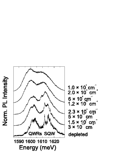
For the gated sample, excitation is performed from the (001)-sample surface. This permits us to observe simultaneously and compare the PL (figure 3) of the QWRs (peak on low energy side) and the SQW (high side) between digital alloy and overgrowth spacer. The MQWs PL occurs at higher energy than the exhibited energy window. Applying a negative gate voltage relative to the electron system, the charge density in the QWRs and in the SQW is reduced. In figure 3, we have converted applied gate voltage into electron density per unit length for the QWRs and per unit area for the SQW. The bottom spectra of figure 3 displays the response for complete depletion as confirmed by a series of PLE measurements. If the depletion voltage is further increased, neither the PL peak position, nor qualitatively the PL lineshape change, which is consistent with a total depletion of the electron systems for the bottom spectra. With decreasing electron density, the PL lines of both the QWRs and the SQW narrow slightly, which is consistent with a reduction of the Fermi wave vector for both the QWRs and the SQW. Note that the estimated electron density of in the SQW exceeds the 2D Mott-density [18]. At low densities, moreover, sharp peaks appear on the PL lines, which we attribute to excitonic, spatially localized recombination. For the SQW (figure 4), one
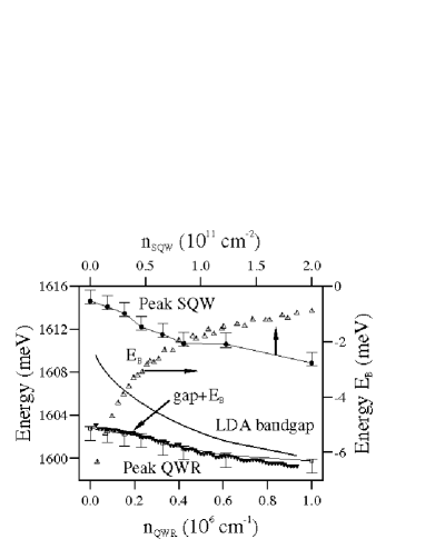
notices a characteristic redshift of the energetic peak position of about , obtained by a simple lineshape fit, as the 2d electron density, , is increased from zero to about . Correcting for the energy shift due to the quantum confined Stark effect [19], determined by self-consistently solving Schrödinger s and Poisson s equation, the residual shift, due to 2D BGR, amounts to about , in good agreement with earlier results for a n-modulation doped quantum well [20]. The indicated tolerance takes into account the uncertainty in determining the real PL peak position, as two PL lines overlap in figure 3.
The principle result of figure 4, however, is the weak variation of the peak position for the QWRs as varies. The overall shift of only about , when the electron density is increased from zero to about , is similar to results found for wires with a two component plasma in high excitation [5].
The observation is in excellent agreement with the variation of the bandgap determined by the LDA calculation when the excitonic screening correction is included. The details of our calculation, which are based on a total free energy functional for the interacting wire-gate system [21] will be discussed in a separate publication [17]. In figure 4 we plot the variation of the translationally invariant band edge, the calculated exciton binding energy and the combination of the two as a function of . Clearly, without the screening of the exciton, the band edge variation disagrees markedly with measurement. The variation of the exciton binding, however, is functionally nearly the inverse of the band edge variation, with variation at low strongest in both cases. The result is a close cancellation and a trend with that recapitulates the data.
A similar cancellation of exciton binding energy and BGR has been derived recently by Das Sarma and Wang [22] using the Bethe-Salpeter equation, for the case of a two-component, neutral plasma (i.e. for ). However one striking contrast between our results and those of Ref. [22] is that, up to our highest density , we find that the electron and hole remain bound (cf. Fig. 4), whereas those authors find a merging of the exciton with the continuum, a so-called “Mott transition,” in the range of . The robustness of the exciton revealed in our calculations emerges from the requirement of orthogonality between the free, screening electrons and those bound to the hole; a constraint which is not maintained in the many-body calculation. Therefore, at least in the case of a one component plasma, we find that the stability of the exciton exceeds that predicted by the conservative Mott criterion.
In addition our calculation employs the full non-linear screening, whereas the many-body calculation [22] assumes linear screening and hence is not valid in the low density limit. Regarding this point, it is in the low density regime where BGR and the excitonic binding energy change most rapidly with density. The result that there remains a strong tendency for the two effects to cancel is therefore suggestive of a fundamental connection between the two processes. The exchange portion of the energy, which dominates at low density, varies as . Therefore a dependence for the screened exciton interaction is suggested, although we do not have a fundamental argument for this.
In conclusion, we have presented photoluminescence measurements of a modulation doped and surface gated T-shaped quantum wire which exhibit a weak dependence of the peak position on the density of conduction band electrons in the wire. We have also reported on density functional calculations for the structure which show a bandgap renormalization of over the range of measured densities. A calculation of the excitonic binding energy and its screening shows a complementary trend to the BGR such that the combined results are largely insensitive to and agree well with the observed line peak. Finally, we find that while the exciton binding weakens with density, it nonetheless remains bound up to , suggesting an excitonic stability well in excess of the Mott criterion.
permanent address: Universität Regensburg, 93040 Regensburg, Germany
REFERENCES
- [1] For reviews, see H. Kalt, Optical Properties of III-V Semiconductors (Springer-Verlag, Berlin, 1996); H. Haug and S. W. Koch, Quantum Theory of the optical and Electronic Properties of Semiconductors (World Scientific, Singapore, 1993).
- [2] S. Schmitt-Rink, D. Chemla and D. A. B. Miller, Adv. in Phys. 38, 89 (1989); R. Cingolani and K. Ploog, ibid. 40, 535 (1991).
- [3] S. Das Sarma, R. Jalabert and S. R. Eric Yang, Phys. Rev. B 39, 5516 (1989); 41, 8288 (1990).
- [4] W. Wegscheider, L. N. Pfeiffer, M. N. Dignam, A. Pinczuk, K. W. West, S. L. McCall and R. Hull, Phys. Rev. Lett. 71, 4071 (1993).
- [5] R. Ambigapathy, I. Bar-Joseph, D. Y. Oberli, S. Haacke, M. J. Brasil, F. Reinhardt, E. Kapon and B. Deveaud, Phys. Rev. Lett. 78, 3579 (1997).
- [6] R. Cingolani, R. Rinaldi, M. Ferrara, G. C. La Rocca, H. Lage, D. Heitmann, K. Ploog and K. Halt, Phys. Rev. B 48, 14331 (1993).
- [7] Ben Yu-Kuang Hu and S. Das Sarma, Phys. Rev. Lett. 68, 1750 (1992); Phys. Rev. B 48, 5469 (1993).
- [8] S. Benner and H. Haug, Europhys. Lett. 16, 579 (1991); B. Tanatar, J. Phys.: Condens. Matter 8, 5997 (1996).
- [9] E. H. Hwang and S. Das Sarma, Phys. Rev. B 58, R1738 (1998).
- [10] L. Pfeiffer, K. W. West, H. L. Stormer, J. P. Eisenstein, K. W. Baldwin, D. Gershoni and J. Spector, Appl. Phys. Lett. 56, 1697 (1990).
- [11] S. Glutsch, F. Bechstedt, W. Wegscheider and G. Schedelbeck, Phys. Rev. B 56, 4108 (1997).
- [12] A. R. Goñi, L. N. Pfeiffer, K. W. West, A. Pinczuk, H. U. Baranger and H. L. Störmer, Appl. Phys. Lett. 61, 1956 (1992).
- [13] T. Someya, H. Akiyama and H. Sakaki, J. Appl. Phys. 79, 2552 (1996).
- [14] R. D. Grober, T. D. Harris, J. K. Trautman, E. Betzig, W. Wegscheider, L. Pfeiffer and K. West, Appl. Phys. Lett. 64, 1421 (1994).
- [15] J. Hasen, L. N. Pfeiffer, A. Pinczuk, K. W. West and B. S. Dennis, Nature 390,54 (1997).
- [16] F. Rossi and E. Molinari, Phys. Rev. Lett. 76, 3582 (1996).
- [17] M. Stopa, unpublished.
- [18] Gerrit E. W. Bauer, Sol. St. Comm. 78, 163 (1991).
- [19] G. Bastard, Wave Mechanics Applied to Semiconductor Heterostructures, Les Ulis Cedex, Les éditions de physique, p. 239 (1998).
- [20] C. Delalande, G. Bastard, J. Orgonasi, J. Brum, H. Liu and M. Voos, Phys. Rev. Lett. 59, 2690 (1987).
- [21] M. Stopa, Phys. Rev. B 54, 13767 (1996).
- [22] S. Das Sarma and D. W. Wang, cond-mat/9905038.