Low-temperature dephasing in disordered conductors: experimental aspects
Abstract
What is the lowest temperature to which one can trace the growth of the dephasing time in low-dimensional conductors? I consider the fundamental limitation, the crossover from weak to strong localization, as well as several experimental reasons for frequently observed saturation of (hot-electron effects, dephasing by external noise). Recent progress in our understanding of the electron-phonon interaction in disordered conductors is also briefly discussed.
1 Introduction
Electron localization and dephasing of the electron wave function are deeply interwoven. This idea was established more than two decades ago, and is widely appreciated now [1, 2]. The quantum interference measurements in the weak localization (WL) regime became a powerful tool for the study of different scattering processes in disordered conductors. As a result of literally hundreds of experiments, the dephasing time has been measured in all dimensions. The earlier progress in this field was summarized in reviews [3, 4]; more recent results can be found in Refs. [2, 5].
The dephasing attracted renewed interest due to rapid development of the quantum information processing (see, e.g. [6]). The relatively short dephasing time in solid-state devices remains one of the major obstacles in the way of implementation of quantum computers. The importance of universal (intrinsic) and non-universal (extrinsic) limitations on the dephasing rate has been emphasized in a recent paper by Mohanty, Jarivala, and Webb [7]. The authors of Ref. [7] addressed the old problem of the low-temperature saturation of , which is observed in essentially all experiments at . On the basis of detailed measurements of in one-dimensional () gold wires, they came to the conclusion that a finite dephasing rate at is intrinsic, and is related to the zero-point fluctuations of the electrons. This issue is important since an intrinsic saturation of would signal a breakdown of Fermi-liquid behavior of low-dimensional conductors in the metallic regime.
This mini-review does not pretend to cover all recent measurements of . Instead, I focus on several problems, which are common for the low-temperature dephasing experiments, and which are relevant to the quest for extra-large . One problem is fundamental: when becomes of the order of the diffusion time over the localization length , the low-dimensional conductors enter the strong localization (SL) regime. In this regime, the hopping rate replaces the dephasing rate. Two other experimental problems are the noise-induced dephasing and overheating of electrons by applied voltage and/or external noise. Recent measurements of the electron-phonon scattering rate in disordered conductors help to clarify the latter problem.
2 Sources of dephasing
The dephasing time is usually extracted from the low-field magnetoresistance [3, 4] and, less often, from the temperature dependence of the universal conductance fluctuations [8, 9]. Measurements of in a variety of 1d, 2d, and 3d metal and semiconductor stuctures have been reported (see [3, 4, 5, 10, 11] and references therein). At present, there is experimental evidence of several ”intrinsic” and ”extrinsic” sources of dephasing. The most important intrinsic mechanisms are:
- the electron-phonon interaction, which governs dephasing at high temperatures111In 3d conductors, this temperature range can be extended down to sub-Kelvin temperatures (see Fig. 5b).;
-the electron-electron interaction, which dominates at low temperatures (typically, below 1-10K for 1d and 2d conductors).
The most common ”extrinsic” sources of dephasing are magnetic impurities and the high-frequency electromagnetic noise in the experimental set-up.
I will focus on the low- regime in 1d and 2d conductors, typical experimental data are shown in Fig.1. The observed dependence can be accounted for by the theory of electron-electron interaction in disordered metals [1, 12]. The theory predicts that in low dimensions, interactions with small momentum and energy transfers are the most efficient dephasing mechanism. These quasielastic electron-electron collisions are equivalent to interaction of an electron with the fluctuating electromagnetic field produced by all the other electrons (dephasing by the equilibrium Nyquist noise). The Nyquist dephasing rate can be expressed as [12]:
| (1) |
| (2) |
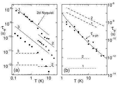
Here is the electron diffusion constant, is the sheet resistance, and is the resistance of a 1d conductor per unit length. The predicted temperature dependences of the dephasing rate [, ] agree very well with the experimental data for many systems, including thin metal films and wires [13, 14, 15, 16, 17, 18, 25, 26], semiconductor structures [27, 28], and even multi-wall carbon nanotubes [29]. Absolute values of for metal wires are usually somehow smaller than the estimates (1) and (2) 222Note that for correct extraction of from the 1d magnetoresistance, one should use the expression for the 1d WL correction calculated for the quasi-elastic dephasing in Ref. [12]. Use of the WL correction for the strongly-inelastic processes [B. L. Altshuler and A. G. Aronov, Sov. Phys. JETP Lett. 33 (1981) 515] would result in overestimation of by a factor of 4 at low , where the Nyquist mechanism dominates [13].(see Figs. 1, 2a, 3b, and 5a).
| (3) |
where is the conductance of a -dimensional system (measured in units of ) on the scale determined by the phase-breaking length . On the ”metallic” side of the WL-SL crossover, where , the electron states are well-defined (). Thus, both 1d and 2d conductors should behave as Fermi-liquid systems over the whole range that corresponds to the WL regime [20]. At the same time, Eq. 3 shows that the WL-SL crossover imposes a fundamental limitation on the increase of the dephasing time: cannot exceed the diffusion time over the localization length. Recent experiments on observation of the Thouless crossover in 1d conductors confirm this prediction [14, 21, 22] (see Fig. 2). All relevant energy scales in 1d conductors become of the same order at the crossover temperature [22]:
| (4) |
Here is the mean level spacing within the localization domain ( is the 1d single-particle density of states), is the Thouless energy, and is the activation energy of the Arrhenius dependence observed in the SL regime.
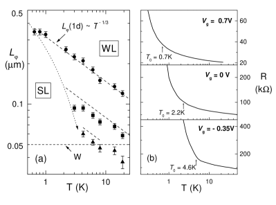
Demonstration of this universality is facilitated by the ”sharpness” of the temperature-driven WL-SL crossover in 1d conductors. It is more difficult to access both the WL and SL regimes for the same 2d sample without changing its parameters.
3 Low-temperature saturation of
The crossover temperature is usually unattainably low for thin metal wires and films (unless their thickness is comparable with the Fermi wavelength [30, 31]). Nevertheless, all experiments with disordered metals and semiconductors show some saturation of at (for references, see [7]). There are several possible causes for saturation of , the most common ones are scattering by localized spins and overheating of the electrons (due to the applied current or to the external noise). A more subtle reason for saturation is noise-induced dephasing without overheating of electrons.
3.1 ”Hot” electrons and the electron-phonon interaction
The first problem is related to the electron-phonon interaction (EPI). At low temperatures, the EPI is the bottleneck in the energy transfer from the electrons to the heat sink, and the electrons can be easily overheated by the measuring current or external noise (another mechanism of heat removal, the heat flow along the sample in cooler leads, will be considered below). Thus, the knowledge of the EPI is essential for the low-temperature dephasing measurements.
The last 15 years have resulted in considerable progress in understanding of the EPI in disordered metals and heavily doped semiconductors. It has been predicted theoretically [33, 34] and tested experimentally [35, 36, 37], that the interactions with transverse phonons are dominant at ( is the wave number of a thermal phonon, is the electron mean free path) (for a review, see [38]). Notice that in the clean case, the electrons interact with longitudinal phonons only. The constants of interaction with transverse phonons can be found from analysis of the term in the dependence for disordered metals [34, 35, 37]. Using the interaction constants, one can estimate the contributions of transverse and longitudinal phonons to the electron-phonon scattering time . These calculations are in good agreement with direct measurements of in thin metal films [37] (see also Fig.5b).
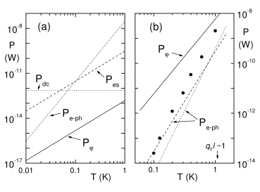
Rapid growth of with decreasing temperature causes a very large thermal resistance between the electrons and the phonons. Figure 4a shows that a sub-pico-watt power can overheat electrons in a 1d wire at . Even smaller values of are sufficient for overheating the 2d electrons in GaAs structures (Fig. 4b). For this reason, a very thorough filtering of all the leads to the sample is required.
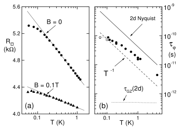
Since both localization and interaction corrections at low depend on the electron temperature only, it is easy to check if the electrons are at the bath temperature: the electron overheating also causes saturation of . Figure 3 shows for 2d Si -doped GaAs structure at and at (the latter magnetic field is sufficiently strong to suppress the temperature dependence of the WL correction) [24]. Saturation of the logarithmic dependence indicates that the electrons were never cooled below 0.1K. The dephasing time plotted for this sample versus the bath temperature demonstrates a clear saturation below (Fig 3); this saturation is less pronounced if one takes into account the electron overheating.
3.2 The noise-induced dephasing
The authors of Ref.[7] have demonstrated that saturation of , observed for 1d Au wires, was not caused by electron overheating or by the spin-spin scattering 333The authors of Ref.[7] ruled out the possibility of conventional spin-flip scattering. However, it has been suggested recently that dephasing by two-level systems (TLS) in the two-channel Kondo regime can cause saturation of in a limited temperature range [47]. This mechanism is non-universal, since the density of the non-magnetic dynamic TLS with an almost degenerate Kondo ground state is both sample- and history-dependent.. It is more difficult, however, to rule out another possibility for the saturation, namely, dephasing by external noise. Indeed, it has been known since the early 80s, that the external high-frequency radiation can induce dephasing [41]; this effect was observed in the experiments [42, 43, 44]. The key point is that dephasing by the rf noise can occur without electron overheating.
What are the experimental conditions for observation of this effect? The phase coherence is destroyed most efficiently by spectral components of the noise with the frequency [41]. The electric field for dephasing at the time scale can be estimated as [41]. For 1d conductors, (see Eq.1), and the noise power sufficient for saturation of below a certain is [14, 19]:
| (5) |
The inflow of the noise energy is balanced by the energy outflow due to two competing cooling mechanisms, the EPI and outdiffusion of hot electrons in cooler leads. The latter mechanism becomes more efficient in relatively short samples at low temperatures [45, 46]. As it is shown in Refs. [14, 19], balancing of the incoming rf noise energy (sufficiently strong for dephasing) by the hot-electron outdiffusion results in a negligible rise of the electron temperature if the total resistance of a wire is less than the quantum resistance . In the experiment [7], the wire resistance was in the range , and one cannot exclude the possibility of rf-noise-induced dephasing without electron overheating (see Fig. 4a). Experiments with wires of a larger could clarify this situation. Such high-resistance wires are also less prone to the noise-induced dephasing, since is proportional to . However, there is a trade-off: longer wires cannot be efficiently cooled by the hot-electron outdiffusion, and restrictions on the measuring current become more severe.
4 Theory of dephasing by quantum fluctuations: comparison with experiment
In an attempt to explain the low- saturation of , it has been suggested that the zero-point fluctuations of electrons contribute to dephasing [7]. Golubev and Zaikin obtained the finite dephasing rate at in all dimensions due to quantum fluctuations of the electric field produced by other electrons [23]. The detailed criticism of this idea, in general, and of the calculations by Golubev and Zaikin, in particular, have been given in Refs. [19, 53]; here we briefly compare the predictions of the theory [23] with the experiment.
According to Ref.[23], the dephasing rate in 3d conductors is limited by , which is comparable with the elastic scattering time . If this were the case, the 3d WL corrections would be completely ”washed out”. Nevertheless, the temperature-dependent WL corrections have been observed in a host of 3d systems (disordered metals [4], metal glasses [11], heavily doped semiconductors [10]). Figure 5b shows that dephasing in 3d metal films is governed by interaction with transverse phonons. The experimental values of exceed the limiting value by 5(!) orders of magnitude. This disagreement is equally strong for both macroscopically homogemeous and inhomogeneous systems (thus, it cannot be attributed to the charging effects [23]), with the parameter (this rules out the argument that the theory [23] disagrees only with the data for systems with ).
Similar disagreement is observed in 2d. On the one hand, the upper limit would preclude observation of the -dependent WL corrections. On the other hand, a well-pronounced temperature dependence of has been observed, and the experimental values of are typically much greater than (Figs. 1b, 3b and 5a). Note, that since is always much smaller than the localization length, this would prohibit the 2d WL-SL crossover. This prediction is also at odds with the experiment [30, 31, 32, 24].
In 1d, the temperature dependence of coincides with the 1d Nyquist dephasing rate (Eq.1) at , and saturates at lower temperatures [23]. This saturation corresponds to the maximum dephasing length , where is the 1d localization length, is the number of transverse channels in the wire. If this were the case, the 1d conductors would not enter the strong localization regime with decreasing temperature. However, the Thouless crossover has been observed for 1d conductors with [14, 21, 22].
5 Conclusions
At present, there is no experimental evidence for an ”intrinsic”, universal mechanism of a finite dephasing rate at . Such evidence could be obtained only if all the known reasons for saturation of were ruled out. In this respect, a useful guideline is provided by the Law of Economy (also known as Ockham’s razor): ”entities are not to be multiplied beyond necessity”. This does not mean, of course, that one cannot expect to encounter new phenomena with a further decrease in temperature. Clearly, the experimental and theoretical study of the low-temperature dephasing will remain an important and exciting field in the future.
I thank Yu. Khavin, P. Echternach, A. Bogdanov, D. Reuter, P. Schafmeister, and A. Wieck for collaboration, and B. Altshuler and I. Aleiner for numerous helpful discussions. This work is supported in part by the ARO-administered MURI grant DAAD 19-99-1-0252.
References
- [1] B. L. Altshuler and A. G. Aronov, in Electron-electron interactions in disordered systems, eds. A. L. Efros and M. Pollak, North-Holland, Amsterdam 1985, p.1
- [2] Y. Imry, Introduction to mesoscopic physics, Oxford University Press, New York 1997
- [3] G. Bergmann, Phys. Rep. 107 (1984) 1
- [4] B. L. Altshuler et al., Sov. Phys. Rev. A9 (1987) 223
- [5] H. Bouchiat, in Mesoscopic Quantum Physics, eds. E. Akkermans et al., Elsevier 1995, p.99
- [6] D. P. DiVincenzo, in Mesoscopic Electron Transport, L. L. Sohn et al. (eds.), Kluwer Academic Publishers, Dordrecht, 1997; A. Steane, Rep. Prog. Phys. 61 (1998) 117
- [7] P. Mohanty, E. M. Q. Jarivala, and R. A. Webb, Phys. Rev. Lett. 78 (1997) 3366
- [8] S. Washburn and R. A. Webb, Rep. Prog. Phys. 55 (1992) 1311
- [9] P. McConville, and N. O. Birge, Phys. Rev. B 47 (1993) 16667
- [10] T. A. Polyanskaya and Yu. V. Shmartsev, Sov. Phys. - Semicond. 23 (1989) 1
- [11] J. S. Dugdale, The Electrical Properties of Disordered Metals, Cambridge University Press, Cambridge 1995
- [12] B. L. Altshuler, A. G. Aronov, and D. E. Khmelnitskii, J. Phys. C 15 (1982) 7367
- [13] P. M. Echternach et al., Phys. Rev. B 48 (1993) 11516
- [14] Yu. B. Khavin, M. E. Gershenson, and A. L. Bogdanov, Phys. Rev. Lett. 81 (1998) 1066
- [15] P. M. Echternach et al., Phys. Rev. B 46 (1992) 10339
- [16] M. Henzler, T. Luer, and J. Heitmann, Phys. Rev. B 59 (1999) 2383
- [17] J. J. Lin and N. Giordano, Phys. Rev. B 33 (1986) 1519
- [18] V. B. Krasovitskii et al., Low Temp. Phys. 21 (1995) 642
- [19] B. L. Altshuler, M. E. Gershenson, and I. L. Aleiner, Physica E 3 (1998) 58
- [20] There are many transverse quantum channels in the conductors that are one-dimensional with respect to the quantum interference effects, and the inter-channel scattering is strong. The physics of these (quasi)-1d conductors is essentially different from the physics of quantum wires; the latter single-channel limit is described by the Tomonaga-Luttinger model.
- [21] M. E. Gershenson et al., Phys. Rev. Lett. 79 (1997) 725
- [22] Yu. B. Khavin, M. E. Gershenson, and A. L. Bogdanov, Phys. Rev. B 58 (1998) 8009
- [23] D. S. Golubev and A. D. Zaikin, Phys. Rev. Lett. 81 (1998) 1074; Physica B 2553 (1998) 164; Phys. Rev. B 59 (1999) 9195; cond-mat/9811185
- [24] M. E. Gershenson, Yu. B. Khavin, D. Reuter, P. Schafmeister, and A. D. Wieck (unpublished)
- [25] S. Wind et al., Phys. Rev. Lett. 57 (1986) 633
- [26] T. J. Thornton et al., Phys. Rev. Lett. 56 (1986) 1198
- [27] B. J. F. Lin et al., Phys. Rev. B 29 (1984) 927
- [28] J. A. Katine et al., Phys. Rev. B 57 (1998) 1698
- [29] C. Schonenberger et al., cond-mat/9905144
- [30] Y. Liu, B. Nease, K. A. McGreer, and A. M. Goldman, Europhys. Lett. 19 (1992) 409
- [31] S.-Y. Hsu and J. M. Valles, Phys. Rev. Lett. 74 (1995) 2331
- [32] F. W. Van Keuls et al., Phys. Rev. B 56 (1997) 13263
- [33] J. Rammer and A. Schmid, Phys. Rev. B 34 (1986) 1352
- [34] M. Yu. Reizer and A. V. Sergeev, Sov. Phys. JETP 63 (1986) 616; Sov. Phys. JETP 65 (1987) 1291
- [35] P. M. Echternach, M. E. Gershenson, and H. M. Bozler, Phys. Rev. B 47 (1993) 13659
- [36] N. G. Ptitsina et al., Sov. Phys. JETP 80 (1995) 960
- [37] N. G. Ptitsina et al., Phys. Rev. B 56 (1997) 10089
- [38] A. V. Sergeev and M. Yu. Reizer, Int. J. Mod. Phys. B10 (1996) 635
- [39] E. Chow et al., Phys. Rev. Lett. 77 (1996) 1143; D. V. Khveshchenko and M. Reizer, Phys. Rev. B 56 (1997) 15822
- [40] P. J. Price, J. Appl. Phys. 53 (1982) 6863
- [41] B. L. Altshuler, A. G. Aronov, and D. E. Khmelnitskii, Solid State Commun. 39 (1981) 619
- [42] S. Wang and P. E. Lindelof, Phys. Rev. Lett. 59 (1987) 1156
- [43] S. A. Vitkalov et al., Sov. Phys. JETP 67 (1988) 1080
- [44] J. Liu and N. Giordano, Phys. Rev. B 39 (1989) 9894; Phys. Rev. B 43 (1991) 1385
- [45] D. E. Prober, Appl. Phys. Lett., 62 (1993) 2119; Phys. Rev. Lett. 75 (1995) 3964
- [46] A. Mittal et al., Surf. Sci. 361/362 (1996) 537
- [47] A. Zawadowski, J. von Delft, and D. C. Ralph, cond-mat/9902176
- [48] A. E. White, R. C. Dynes, and J. P. Garno, Phys. Rev. B 29 (1984) 3694
- [49] M. E. Gershenson et al., Sov. Phys. - JETP 58 (1983) 167
- [50] F. Komori, S. Kobayashi, and W. Sasaki, J. Phys. Soc. Jpn. 52 (1983) 4306
- [51] A. G. Aronov et al., Sov. Phys. - JETP 60 (1984) 554
- [52] W. Eschner, W. Gey, and P. Warnecke, in Proc. of the 17-th Int. Conf. on Low Temp., eds. U. Eckern et al., Elsevier 1984, p.497
- [53] B. L. Altshuler, I. L. Aleiner, and M. E. Gershenson, Waves Random Media, 9 (1999) 201; Phys. Rev. Lett. 82 (1999) 3190