[
Electron-Assisted Hopping in Two Dimensions
Abstract
We have studied the non-ohmic effects in the conductivity of a two-dimensional system which undergoes the crossover from weak to strong localization with decreasing electron concentration. When the electrons are removed from equilibrium with phonons, the hopping conductivity depends only on the electron temperature. This indicates that the hopping transport in a system with a large localization length is assisted by electron-electron interactions rather than by the phonons.
pacs:
72.15.Rn, 72.20.Ee, 72.20.Ht]
Lowdimensional conductors demonstrate the crossover from weak localization (WL) to strong localization (SL) with decreasing electron concentration and/or increasing disorder. The WL regime, where electron motion is diffusive, and the localization and interaction effects reveal themselves as quantum corrections to the conductivity, is well-understood now (for an experimental review, see [1]). In the SL regime, electron transport is due to activated hopping between the localized states [2]. The mechanism of this hopping is still under debate. On one hand, it is common wisdom to treat this hopping as phonon-assisted (see, e.g., [2, 3, 4]). On the other hand, recent observations suggest that hopping is assisted by some other mechanism rather than phonons [5]. The idea of hopping due to electron-electron scattering in conductors with a large localization length has been also discussed in several theoretical papers (see, e.g. [6, 7]).
In this Letter, we study the non-ohmic effects in the conductivity of a two-dimensional (2d) electron gas on both sides of the WL-SL crossover. It is shown that in either regime, diffusive or hopping, the nonlinear effects are well described by the model of ”hot” electrons, and electron transport is controlled by the electron temperature rather than the phonon one. This indicates that hopping transport on the ”insulating” side of the crossover is governed by the electron-electron interactions.
The resistance of a two-dimensional (2d) -doped structure has been studied as a function of the magnetic field and the bias current in the temperature range . A single -doped layer with concentration of donors x is under the surface of the MBE-grown undoped . Two identical devices were formed by photolithography and wet etching on a chip with dimensions xx the area of each device between the voltage leads was x . The electron concentration can be tuned by applying the voltage to the gate electrode on top of each device. The measurements were done in the four-probe configuration using a low-frequency () lock-in technique in the range , and a dc current source and an electrometer for .
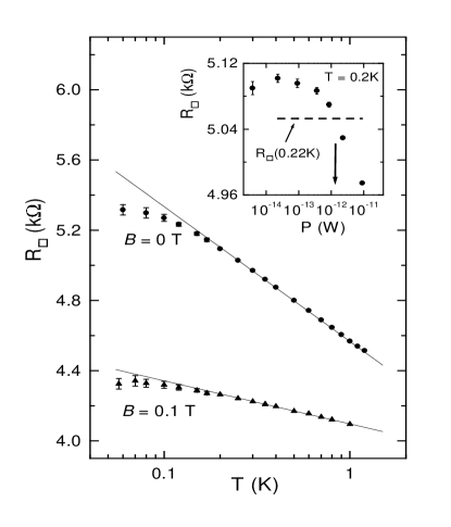
We have observed the WL-SL crossover with reducing the electron concentration (see the inset in Fig.3); the detailed analysis of the crossover will be given elsewhere [8]. The ”zero-bias” dependences are shown on both sides of the crossover in Figs.1 and 2. The logarithmic dependences , observed in the WL regime, are caused by the weak localization and interaction effects at , and by interaction only at (this field is sufficiently strong to suppress the -dependence of the WL correction) [1]. Because of insufficient filtering of the external noise, is saturated at . This indicates that the electrons were never cooled below in the WL regime.
Electron transport becomes activated on the ”insulating” side of the WL-SL crossover. The temperature dependence of the sheet resistance is usually fitted in this regime as
| (1) |
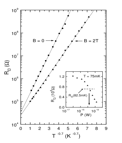
several combinations of and have been reported for different 2d systems [3, 4, 5, 9, 10]. A good fit for our data at is provided by Eq.(1) with and (see Fig.2). Notice that in the SL regime, where the resistance at low is by larger than in the WL regime, saturation of is absent [11].
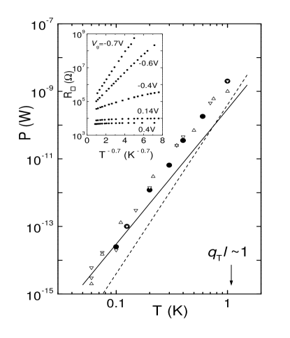
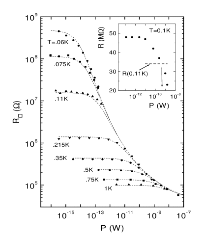
With increase of the bias current, the I-V curves become nonlinear in both WL and SL regimes. The insets in Figs. 1 and 2 show the resistance at a fixed mixing chamber (MC) temperature versus the bias current power, . It is instructive to compare for both regimes the power that causes the decrease of that is equivalent to increase of by a fixed percentage (below we choose ). The procedure is illustrated by the insets of Figs.1 and 2. The resistance, measured at a fixed and different , has been compared with the zero-bias . The corresponding values of , shown by the vertical arrows in the insets, are plotted for in Fig.3. The same measurements have been repeated in the SL regime for several values of . Within the experimental accuracy, no dependence was observed in the range (the data for are shown in Fig.3). Below we analyze separately the data for the WL and SL regimes.
The WL regime. The low-temperature nonlinear effects in the WL regime have been intensively studied in recent years [12, 13], they are accounted for by the electron overheating. The hot-electron model assumes that the non-equilibrium electron distribution function can be characterized by an effective electron temperature , the electron-phonon interaction is the bottleneck in the energy transfer from the electrons to the heat sink, and the phonons are in equilibrium with the heat sink (the phonon temperature is the same as ). One can find from comparison of measured at different currents, provided the zero-bias depends on only.
All these assumptions can be justified in our experiment. Indeed, at sub-Kelvin temperatures, the electron-electron scattering rate is much greater than the electron-phonon one; this allows to introduce . Both WL and interaction corrections are only -dependend, since the dominant phase-breaking mechanism is the quasi-elastic electron-electron scattering [8, 14, 15]. We have also verified that the phonons in the GaAs chip remain in equilibrium with the mixing chamber (in other words that the resistance drop at large is not due to heating of the whole chip relative to the thermometer monitoring the MC temperature). In this test, the zero-bias resistance of one of the devices (a phonon ”thermometer”) was measured at as a function of the Joule heat released in the other device on the same chip (a ”heater”) (see the inset of Fig.4). The power required for a -increase of the temperature of the whole chip is by 3.5 orders of magnitude greater than the power that causes nonlinear effects in the experiments when the same device combines the functions of the ”heater” and the ”thermometer”.
Since the outdiffusion of ”hot” electrons in cooler leads can be neglected for our samples at [16, 13], the energy is transferred from electrons to the heat sink due to the electron-phonon interaction only. At , the device enters the hydrodynamic regime [ is the wave vector of a transverse phonon, is the transverse sound velocity ( for GaAs), the electron mean free path at ]. The low- data are in agreement with calculations of the energy flow from the 2d electrons in GaAs to the bulk phonons due to the piezoelectric coupling at [17]:
| (2) |
where is the sheet resistance, and is the area of the device (the solid line in Fig.3). At , the experimental values of exceed by a factor of both (2) and the result for the clean case [18]:
| (3) |
(the dashed line in Fig.3). Our experimental dependence is consistent with the data for the GaAs heterostructures with larger , obtained in Ref.[13] at .
The SL regime. The striking similarity of the dependences obtained in the ”metallic” and ”insulating” regimes indicate that the mechanism of nonlinearity is also the same on both sides of the WL-SL crossover. Figure 4 shows that the hot-electron model describes very well the dependences in the SL regime [19]. It might be, of course, just a coincidence: some field effects in the SL regime could produce, in principle, similar nonlinearities. However, measurements in the magnetic field rule out this possibility. Indeed, all the models of non-ohmic hopping transport predict the dependence of the characteristic electric field on the localization length [20]. In the magnetic field, which breaks the time-reversal symmetry within the localization domain, increases significantly [21]: the exponentially strong negative magnetoresistance, which has been observed for 1d and 2d -doped GaAs structures (see Fig. 2), is a signature of this -induced growth of [22, 14, 8]. Despite of the increase of in strong magnetic fields, no dependence was observed [23].
The applicability of the hot-electron model to the SL regime indicates that: a) the electron-phonon interaction remains the same on the ”insulating” side of the crossover, and b) the resistance in the SL regime depends on the electron temperature only. The former conclusion is not very surprising. Indeed, the localization length, which can be estimated from the magnetoresistance [22, 14, 8], is large close to the crossover ( for ). The electron motion is still diffusive at distances , with the values similar to that in the WL regime. Since even at , one should not expect strong modification of the electron-phonon interaction on the ”insulating” side of the crossover. The latter conclusion, however, implies that the hopping transport is not phonon-assisted, instead, it is caused by electron-electron interactions.
Recently, the authors of Ref. [5] came to a similar conclusion that hopping in GaAs/AlGaAs heterostructures is not phonon-assisted. This conclusion was based on analysis of the prefactor in Eq. (1). Indeed, is expected to depend on temperature and material properties for the phonon-assisted hopping. Instead, the experimental values are material-independent. They are usually close to the quantum resistance [4, 5, 9, 10]; this value is by several orders of magnitude smaller than the estimate for the phonon-assisted transport. In our experiment, is also close to for both and strong magnetic fields (see Fig. 2).
Previously, the hot-electron model has been applied to the non-ohmic effects in hopping conductivity of three-dimensional heavily-doped Ge [23]. Our 2d structures have two important features that help to attribute unambiguously the observed nonlinear effects to the electron overheating: a) observation of the WL-SL crossover allows direct comparison with the well-understood ”metallic” regime, and b) for the 2d electron gas embedded in bulk GaAs, it is much easier to maintain equilibrium between the phonons and the heat sink than in the case of the 3d uniformly-doped samples.
To summarize, we have shown that the non-ohmic effects in the conductivity of 2d Si-doped GaAs structures, observed on both sides of the WL-SL crossover, are caused by the electron overheating. The heat flow from the hot 2d electrons to equilibrium 3d phonons in the WL and SL regimes is well described by recent calculations for the piezoelectric coupling in the hydrodynamic regime [17]. The conductivity in the hopping regime depends on the electron temperature rather than the phonon one, similar to the WL regime. This observation provides strong evidence that electron hopping in disordered systems with a large localization length is assisted by the electron-electron interactions.
We thank E. Abrahams, B. Altshuler, I. Aleiner, B. Shklovskii, M. Raikh, M. Reizer, and B. Spivak for helpful disccusions. This work was partially supported by ARO-administered MURI grant DAAD 19-99-1-0252 and by the Rutgers Office of the Research and Sponsored Programs. D. R. gratefully acknowledges financial support of the DFG Graduiertenkolleg 384.
REFERENCES
- [1] B. L. Altshuler et al., Sov. Phys. Rev. A9, 223 (1987).
- [2] B. I. Shklovskii and A. L. Efros, Electronic Properties of Doped Semiconductors (Springer, Berlin 1984).
- [3] G. Ebert et al., Solid State Comm. 45, 625 (1983).
- [4] F. W. Van Keuls et al., Phys. Rev. B 56, 1161 (1997); ibid 56, 13263 (1997).
- [5] S. I. Khondaker et al., Phys. Rev. B 59, 4580 (1999).
- [6] D. G. Polyakov and B. I. Shklovskii, Phys. Rev. B 48, 11167 (1993).
- [7] T. V. Shahbazyan and M. E. Raikh, Phys. Rev. B 53, 7299 (1996).
- [8] M. E. Gershenson, Yu. B. Khavin, D. Reuter, P. Schafmeister, and A. D. Wieck, unpublished.
- [9] S-Y. Hsu and J. M. Valles, Phys. Rev. Lett. 74, 2331 (1995).
- [10] G. Martinez-Arizala et al., Phys. Rev. Lett. 78, 1130 (1997).
- [11] A plausible reason for absence of the saturation in the SL regime is that the noise voltage applied to the device is independent of the resistance for sufficiently large ( even in the WL regime). Since the noise power required for electron overheating is the same in both WL and SL regimes, the electron temperature is much less affected by the noise in the SL regime, where is greater by than that in the WL regime.
- [12] E. M. Gershenzon et al., Sov. Phys. JETP 59, 442 (1984); M. L. Roukes et al., Phys. Rev. Lett. 55, 422 (1985); A. K. M. Wennberg et al., Phys. Rev. B 34, 4409 (1986); G. Bergmann et al., Phys. Rev. B 41, 7386 (1990); F. C. Wellstood et al., Phys. Rev. B 49, 5942 (1994); M. Kanskar and M. N. Wyborn, Phys. Rev. B 50, 168 (1994); M. Henny et al., Appl. Phys. Lett. 71, 773 (1997); R. J. Zieve et al., Phys. Rev. B 57, 2443 (1998).
- [13] A. Mittal et al., Surf. Sci. 361/362, 537 (1996); A. Mittal, in Quantum Transport in Submicron Structures, Kluwer Academic Publishers, Dordrecht, 1996.
- [14] Yu. B. Khavin, M. E. Gershenson, and A. L. Bogdanov, Phys. Rev. B 58, 8009 (1998).
- [15] B. L. Altshuler, A. G. Aronov, and D. E. Khmelnitskii, J.Phys. C 15, 7357 (1982).
- [16] D. E. Prober, Phys. Rev. Lett. 75, 3964 (1995).
- [17] E. Chow et al., Phys. Rev. Lett. 77, 1143 (1996); D. V. Khveshchenko and M. Reizer, Phys. Rev. B 56, 15822 (1997).
- [18] P. J. Price, J. Appl. Phys. 53, 6863 (1982).
- [19] Note that the non-ohmic behavior in strong electric fields have been observed for 1d wires fabricated from Si -doped GaAs [14]. The ”threshold” power in 1d is by 2-3 orders of magnitude smaller than the power required for overheating of electrons, and the 1d dependence is quite different than that in 2d. A very low threshold of nonlinearity in 1d is due to the anomalously ”long” hops with exponentially large resistance, which cannot be ”by-passed” in one-dimensional geometry (R. A. Serota et al., Phys. Rev. B 33, 8441 (1986); M. E. Raikh and I. M. Ruzin, Sov. Phys. JETP 68, 642 (1989)).
- [20] B. I. Shklovskii et al., in Transport, Correlations and Structural Defects, edited by H. Fritzsche (World Scientific, Singapore, 1990), p. 161; S. Marianer and B. I Shklovskii, Phys. Rev. B 46, 13100 (1992).
- [21] K. B. Efetov and A. I. Larkin, Sov. Phys. JETP 58, 444 (1983); I. V. Lerner and Y. Imry, Europhys. Lett. 29, 49 (1995).
- [22] M. E. Gershenson et al., Phys. Rev. Lett. 79, 725 (1997).
- [23] N. Wang et al., Phys. Rev. B 41, 3761 (1990); E. Aubourg et al., J. Low Temp. Phys. 93, 289 (1993); J. Zhang et al., Phys. Rev. B 57, 4472 (1998); J. Soudee et al., J. Low Temp. Phys. 110, 1013 (1998).