SPONTANEOUS VS. PIEZOELECTRIC POLARIZATION IN III-V NITRIDES: CONCEPTUAL ASPECTS AND PRACTICAL CONSEQUENCES
Abstract
Macroscopic polarization plays a major role in determining the optical and electrical properties of nitride nanostructures via polarization-induced built-in electrostatic fields. While currently fashionable, this field of endeavour is still by far in its early infancy. Here we contribute some clarifications on the conceptual issues involved in determining built-in fields in III-V nitride nanostructures, sorting out in particular the roles of spontaneous and piezoelectric polarization.
pacs:
Subject classification: 73.90+f,77.65-j,77.90+k,S7.14I INTRODUCTION
Macroscopic polarization in low-symmetry crystals is well known in the ferroelectrics community. Outside that community, it was so far held for a curiosity devoid of practical, let alone technological, relevance. In particular, it was known [1] that a large spontaneous polarization (henceforth SP), at most an order of magnitude smaller than the giant values of ferroelectric perovskites, was present in some wurtzite semiconductors, but due to their minor technological relevance compared to zincblende III-V arsenides or phosphides, this issue was largely overlooked outside a limited circle of specialists.
Such state of affairs has changed after first-principles calculations [2] provided evidence of the considerable SP and larger-then-usual piezoelectric coupling constants of wurtzite III-V nitrides. Because of the huge importance of the latter as materials for optoelectronic devices in the blue–UV range [3], the issue of spontaneous polarization fields was brought to a larger community.
The obvious relevance of polarization in nitrides is due to the fact that it induces large (MV/cm) built-in electrostatic fields in layered nitride nanostructures, as first shown in Ref. [4]. These fields affect dramatically the optical and electrical properties of those structures [5-14]. Quite a flurry of activity has recently revealed a host of new and unexpected effects: to name but some, Stark-like red shifts in recombination and absorption energies for increasing quantum well widths [5, 6, 7, 8, 9], concurrent suppression of oscillator strength [6, 8, 9], ensuing anomalies in recombination dynamics [6, 10, 11, 12], and their interplay with charge injection [8, 9, 13] driving a recovery of oscillator strength and a blue back-shift of transition energies, “self-doping” effects at HEMT heterointerfaces [14], have been demonstrated theoretically and experimentally.
In view of these exciting developments, it is likely that most of the potentially observable polarization-related effects in nitrides are still to be dreamt about. It is safe to state, in any event, that conceptual clarity on the determination of the electric fields produced by polarization, and in particular by SP, is a must if we are to understand and exploit these effects in practical applications. To mention just a pair of issues, the built-in fields depend on boundary conditions and on device design (number of quantum wells, thickness, composition, contacts, etc.); also, the field values and sign patterns are not those expected if only piezoelectricity is considered. This work therefore aims at clarifying some of these subtle questions, focusing on three inter-related systems, i.e. large samples, multi-quantum-wells (MQWs), and isolated quantum-wells (QWs).
II SPONTANEOUS VS. PIEZOELECTRIC
Spontaneous polarization and piezoelectric constants can be reliably determined [15] via simple electronic structure calculations based on the Berry geometric quantum phase concept. We start by discussing our recent result thereon [2], which are summarized in Figs. 1 and 2. The values calculated ab initio are for III-N binaries (AlN, GaN, InN) only; since direct calculations for the alloys are not yet available, an estimate of the SP in AlxInyGa(1-x-y)N alloys was obtained by Vegard interpolation:
| (1) | |||||
| (2) |
similar relations holding for the piezoelectric constants. Thus, the triangle in Fig. 1 borders the (theoretical) SP values achievable in a general III-N alloy as a function of in-plane lattice constant. The triangles in Fig. 2 border the accessible values of the two piezoconstants relevant to -plane epitaxial strains. The large range of accessible polarizations and lattice constants is due to the concurrent large lattice mismatch between GaN and InN on one side, and the very large SP in AlN on the other.
Three main points are evident from the data reported. First, the piezoelectric constants are an order of magnitude larger than in other III-V’s, and reversed in sign. Second, for basal-plane strains typical of epitaxial wurtzite nitride multilayers (2-5%), SP is comparable to, or larger than piezoelectric polarization. Therefore, SP is all but negligible in any typical III-V nitride nanostructures. Third, GaN has nearly the same SP as InN, but a large lattice mismatch to it; on the other hand, AlN has a SP about three times larger than GaN, but a much smaller mismatch. This implies that InGaN/GaN structures will tend to be mostly influenced by piezoelectricity, whereas in AlGaN/GaN systems, SP effects will be dominant. Mixed regimes can also occur, which we will come back to in Sec. V.
III MASSIVE SAMPLES
By elementary electrostatics, polarization and electrostatic field are related by
| (3) |
where is the displacement field, the macroscopic polarization, and the static dielectric constant. The latter have been calculated [16] to be 10.31, 10.28, and 14.61 for AlN, GaN, and InN respectively; the value for generic alloys are estimated by Vegard interpolation. The polarization in Eq. 3 is known as transverse, and it is the sum of the spontaneous and piezoelectric polarization contributions: . The displacement field is determined by the free-charge distribution in the material:
| (4) |
with the electron charge, and and the hole and electron densities, respectively. The evaluation of the electric field inside the semiconductor requires in general a self-consistent solution of Eq. 3 and 4 as outlined in Refs. [8] and [9]. However, many cases can be discussed without explicit calculations, an useful exercise especially in the low free-carrier–density limit.
An interesting such case is the evaluation of polarization effects in large, massive samples. In effect, misunderstanding the role of the displacement field in massive samples leads to predicting wrong electrostatic fields in a MQWs system. At the outset, let it be pointed out that a strong polarization field in a III-V nitride massive sample does not imply the existence of a macroscopic electrostatic field over the whole sample. Qualitatively, since such an electric field would produce (at non-zero temperature) a persistent current due to thermally generated intrinsic carriers, and because this current cannot be sustained indefinitely, the electric field inside a massive sample must be zero. One deduces thereforth that the displacement field in the sample is
| (5) |
For a neutral (albeit polarized) sample, displacement field conservation across the surface would imply an electric field in the vacuum off the sample surface. Of course this is unrealistic, as outside the sample , , and must all vanish. The SP discontinuity across the surface must be counterbalanced by an equal change in the displacement field. Thus, near the surface of our sample, there exists a region where the free-carriers distribution satisfies
| (6) |
with the thickness of the surface region, which may range easily in the hundreds of Å. In this region the free carriers will constitute an approximately two-dimensional electron gas (2DEG) whose areal density equals the SP. The electric field in this region depends strongly on material parameters and on surface states. It can be concluded however that at distances in excess of from the surface (or, in the case of devices, the interface with contacts, buffers, caps, etc.), the electric field will be zero, and the polarization will equal , as will the displacement field. This is the starting point to discuss MQWs.
IV MULTI-QUANTUM-WELLS
As pointed out above (especially in a semi-insulating sample) it can be safely assumed that the displacement field in a large sample is uniform all over the crystal, and equal to , and . If a sequence of QWs, of fixed composition, is now inserted in the (otherwise homogeneous) sample, the electric field inside the generic -th layer (either QW or barrier) is given by:
| (7) |
with and the total polarization and dielectric constant in layer .
If the displacement field is constant, i.e. if Eq. 5 holds, the electric field in the -th layer is
| (8) |
where is the SP in the massive sample material, which now functions locally as barrier material. The field is then zero in the barriers, which are made up of unstrained material with spontaneous polarization , while each QW in the series is subject to the same electric field . A potential drop given by
| (9) |
will thus occur in the generic -th well of thickness .
Now Eq. 5 holds only subject to the following
four constraints:
i) the Debye-Hückel screening length is at least larger
than, say, the MQW region thickness;
ii) the QWs are far enough from any interface with the
outer world that the surface effects mentioned in
the previous Section are negligible;
iii) none of the , nor their sum, must exceed
the band gap energy of the well material:
| (10) |
iv) the well-barrier interfaces are free of interface states.
These requirements are typically met in nitride MQWs, except for condition (iii), which breaks down if the QWs form a sufficiently thick superlattice. Thereby, a self-consistent calculation explicitly accounting for free carriers must be performed. To approximately enforce condition avoiding cumbersome calculations, it is convenient to approximate Eq. 10 applying periodic boundary conditions,
| (11) |
where the sum runs over all layers in the MQW, in particular including the barrier layers. Thereby the displacement field is determined subject to the condition of zero average electric field in the MQW region. The maximal error in the predicted fields due to using Eq. 11 instead of Eq. 10 is of the order of , with the overall thickness of the superlattice; hence this approximation becomes exact in the limit of very thick superlattices. The error may be of course smaller depending on the specific conditions in the device (doping, contacts, etc.).
Substituting Eq. 7 in Eq. 11, the displacement field is then obtained:
| (12) |
Plugging this back into Eq. 7 gives a simple expression for the field in the generic well or barrier of the MQW, namely
| (13) |
with sums running on all layers (including the -th). This is a general expression for any thickness of wells and barriers in a generic superlattice or MQW, which reduces to the formulas in Ref. [9] assuming a single type of well and barrier.
It is to be noted again that in this case the fields are non-zero both in the wells and the barriers. Typically, the sign of the barrier field will be opposite to that of the well, leading to an effectively triangular confinement potential, which favors transfer of confined electrons into the barrier layer on one side of the well, which may lead to anomalous effects in excitonic transitions [11].
In practice, if the conditions discussed above are satisfied for a specific system, the properties of the latter can be calculated by simply solving a Schrödinger equation for the compositional potential of the superlattice with the built-in fields as given by Eq. 13. Of course, this is emphatically not the case in general, because of e.g. doping, excitation, boundary conditions, etc. A self-consistent solution as outlined e.g. in Refs. [8] and [9] will be needed.
V ISOLATED QUANTUM WELLS
Consider now a single QW of material A; let the latter have dielectric constant and spontaneous polarization , and the QW made thereof be strained so as to be subject to a piezoelectric polarization . The total polarization in the QW is then . The well is embedded in an extended, insulating, and unstrained material with spontaneous polarization . According to Eq. 7, the field in the QW is
| (14) | |||||
| (15) |
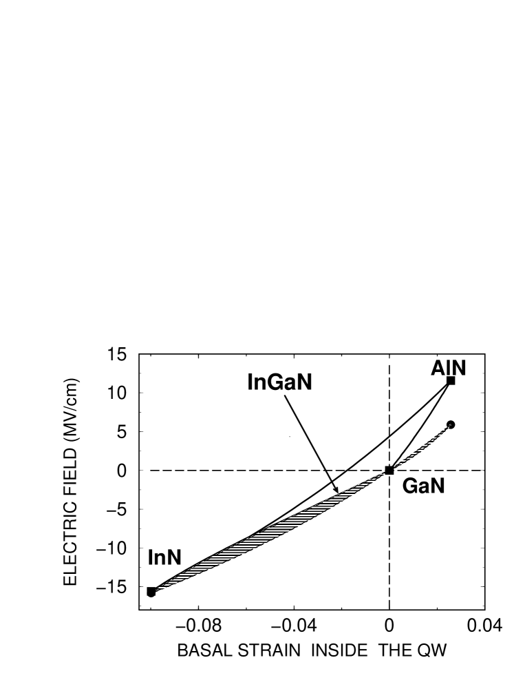
At variance with conventional III-V’s (having no SP), an additional term appears, due solely to the difference in the SP between the QW active layer and the barrier material [17]. This additional term has far-reaching consequences, and can be used to tune the value of the electric field inside the QW. In Fig. 3 we depict the value of the electric field and of its purely piezoelectric component vs in-plane strain for an AlInGaN QW embedded in GaN. Without SP, the values of the electric field inside the QW would fall into the hatched region delimited by dashed lines. The inclusion of SP gives rise to a different, wider accessible region, especially for small strains. The region in question is white and delimited by a continuous line. On the negative strain side of Fig. 3, this region barely touches the upper side of the piezoelectric region, and shrinks becoming a line for large strains. The various region boundaries are curved due to the quadratic dependence of the piezoelectric component on alloy composition (through [piezoconstants][strain] terms).
Several features are worth a mention. First, the two regions do not overlap, i.e. for any composition the total field differs from its pure piezoelectric component (this of course is due to the fact that never vanishes). This difference is rather dramatic for positive strains, i.e. in Al-rich alloy wells. A noticeable exception to this general behavior is that of GaN/InGaN QWs. These correspond to the region where the total and piezo field regions in Fig. 3 (almost) touch each other: in that case indeed, as InN has nearly the same SP as GaN, the SP difference between barrier and active layer, and hence , is negligible with respect to the piezoelectric term. That is why early investigations on GaN/InGaN MQWs [5] yielded results in good agreement with theory even though SP was neglected. Second, without SP the electric field is zero at zero strain (the typical situation in zincblende III-Vs). This is no more the case in III-V nitrides, where SP is an additional degree of freedom potentially producing fields up to 4 MV/cm at zero strain. This requires growing AlInGaN with appropriate compositions, which appears to be difficult because of thermodynamic solubility constraints; however, fields of several hundreds of KV/cm can be achieved already at minute Al and In concentrations, which may perhaps become accessible in the future. Third, last but not least, SP provides a handle for reducing or even, in principle, zeroing the field in strained QWs [9]. Specifically, this occurs on the zero field line in Fig. 3. This can be a breakthrough for the many applications needing a good confinement, but at the same time no built-in field in the active region. The same considerations on growth hold as in the previous point.
VI Summary and acknowledgements
In conclusion, SP can be considered as a degree of freedom to tune the value of the polarization-induced electric fields in QW systems. It was shown, for a GaN/AlInGaN QW, that fields up to 4MV/cm can be obtained in absence of strain, and that, conversely, a vanishing field can also be obtained, despite lattice mismatch, for judicious choices of composition and strain.
Support from the PAISS program of INFM is acknowledged. VF thanks the Alexander von Humboldt-Stiftung for supporting his stay at the Walter Schottky Institut.
REFERENCES
- [1] M. Posternak, A. Baldereschi, A. Catellani, and R. Resta, Phys. Rev. Lett. 64, 1777 (1990); A. Dal Corso, M. Posternak, R. Resta, and A. Baldereschi, Phys. Rev. B 50, 10715 (1994).
- [2] F. Bernardini, V. Fiorentini, and D. Vanderbilt, Phys. Rev. B 56, R10024 (1997).
- [3] See e.g. O. Ambacher, J. Phys. D: Appl. Phys. 31, 2653 (1998).
- [4] F. Bernardini and V. Fiorentini, Phys. Rev. B 57, R9427 (1998).
- [5] T. Takeuchi et al., Jpn. J. Appl. Phys. 36, L382 (1997).
- [6] J. Im et al., Phys. Rev. B 57, R9435 (1998).
- [7] R. Langer et al., Appl. Phys. Lett. 74, 3827 (1999).
- [8] F. Della Sala et al., Appl. Phys. Lett. 74, 2002 (1999).
- [9] V. Fiorentini et al, Phys. Rev B. 60, in print (1999).
- [10] S. F. Chichibu et al., Appl. Phys. Lett. 73, 2006 (1998).
- [11] B. Gil et al., Phys. Rev. B 59, 10246 (1999); P. Lefebvre et al., Phys. Rev. B 59, 15363 (1999).
- [12] R. Cingolani et al., to appear.
- [13] L.-H. Peng, C.-W. Huang, and L.-H. Lou, Appl. Phys. Lett. 74, 795 (1999).
- [14] O. Ambacher et al., J. Appl. Phys. 85, 3222 (1999).
- [15] R. D. King-Smith and D. Vanderbilt, Phys. Rev. B 47, 1651 (1992).
- [16] F. Bernardini, V. Fiorentini, and D. Vanderbilt, Phys. Rev. Lett. 79, 3958 (1997); F. Bernardini and V. Fiorentini, Phys. Rev. B 58, 15292 (1998).
- [17] Note in passing that an equivalent result is obtained from Eq. 13 in the limit of infinite barrier.