[
Coulomb blockade in low mobility nanometer size Si:MOSFETs
Abstract
We investigate coherent transport in Si:MOSFETs with nominal gate lengths 50 to 100nm and various widths at very low temperature. Independent of the geometry, localized states appear when and transport is dominated by resonant tunnelling through a single quantum dot formed by an impurity potential. We find that the typical size of the relevant impurity quantum dot is comparable to the channel length and that the periodicity of the observed Coulomb blockade oscillations is roughly inversely proportional to the channel length. The spectrum of resonances and the nonlinear I-V curves allow to measure the charging energy and the mean level energy spacing for electrons in the localized state. Furthermore, we find that in the dielectric regime the variance of the logarithmic conductance is proportional to its average value consistent with one-electron scaling models.
pacs:
73.23.-b, 73.23.Hk, 72.15.Ra]
After the pioneering work of Scott-Thomas et al [1], Coulomb blockade in quantum dots formed by an impurity potential has been studied in quasi 1D wires or point-contact geometries [2, 3]. In comparison with lithographically defined lateral quantum dots, impurity quantum dots (IQD) contain typically fewer electrons. Downscaling the size of the IQD allows to operate a silicon based single electron quantum dot transistor even at room temperature [4][5]. In the opposite case of wires, i.e. in disordered thin and wide insulating barriers, no Coulomb blockade oscillations have been reported up to now. Resonant tunneling through single ionized donor potentials is responsible for electron transport in disordered thin insulating barriers. This has been studied in the deeply insulating regime of large thin barriers formed by depleting electrostatically a semiconductor under a gate [6], or in thin amorphous silicon tunnel barriers [7]. Interaction between distant impurity states in the channel have been revealed by peculiarities of the nonlinear transport. However, a single ionized donor potential cannot accomodate many electrons without becoming screened.
We report for the first time Coulomb oscillations in very short MOSFETs with source drain distance less than m and width much larger than . Contrarily to quasi 1D wires, where the size of the IQD is somewhat arbitrary, we will show that the diameter of the IQD is comparable to the source drain distance and that on resonance the conductance g in quantum units is close to one. Furthermore we demonstrate that the fluctuations of the conductance characterized by are proportional to the mean value , rather independent of geometry. Such an observation is consistent with one-parameter noninteracting scaling models of the metal-insulator transition. Our experimental findings suggest that interactions do not destroy this one-parameter description.
The devices are MOSFETs on the (100) surface of silicon doped to a level of for the 100nm series and of for the 50nm series. The gate oxyde thickness is only for the 100nm series and for the 50nm series. This screens strongly Coulomb interactions in the inversion layer. Source and drain consist of highly ion implanted regions (). The polysilicon gate has a length of 100nm or 50nm and the transverse dimension varies between 300 nm and 25 . The effective channel length between source and drain is somewhat smaller than the geometrical gate length due to extension regions (). is estimated to be of order 25 nm and 75 nm in the two cases considered here. The room temperature mobility is for the 100nm series and for the 50nm series. The source-drain current is measured for a source-drain voltage as a function of the gate voltage using a standard low-frequency lock-in technique. The characteristics is linear for this value of even at the lowest temperature, independent of . The sample is inside a copper box thermally anchored to the mixing chamber of a dilution refrigerator. About 2 meters of Thermocoax Philips [8] on each side of the sample provide the contact to the lock-in amplifier.
Figure 1 shows the source-drain conductance in quantum units versus in three samples of gate length differing only by the width. At a temperature of mK, we observe reproducible conductance fluctuations as a function of gate voltage which persist up to K at small . Depending on the value of the conductance these fluctuations evolve differently with temperature: If the fluctuations are gaussian around their mean value and poorly sensitive to temperature below T=4.2K. This characterizes universal conductance fluctuations in the diffusive regime not further considered here. If , fluctuations evolve into sharp resonances at very low temperature (dielectric regime). In the diffusive regime, the linear increase of the conductance with the gate voltage permits to evaluate the mobility : if and do not depend on . We find for in the sample, for in the sample and for in the sample (at low temperature). These mobilities are weak reflecting a strong short range disorder and a mean free path of order . The measured capacitance to gate coincides with the theoretical estimations: (for ). A variation of induces for the 100nm series ( for the 50nm series) [9].
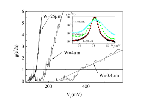
Typical conductance resonances in the dielectric regime are well fitted over 3 orders of magnitude (see inset of Fig.1) by the standard relation for the thermally broadened resonant tunneling regime:
| (1) | |||||
| (2) |
with , and . is the intrinsic linewidth and is the gate voltage at the resonance. is the variation of the Fermi energy. is the effective electron temperature. means that the localized state is equally connected to the source and the drain. If not, the resonant conductance would be exponentially smaller[10]. From , we estimate an approximately constant density of states in the channel , which is reduced by a factor 4 compared to the metallic 2D density of states. This is due to Lifshitz tails induced by disorder at the bottom of the conduction band.
The central result in Fig. 1 is that the onset of diffusive transport is essentially independent of the width of the sample. It always occurs when the total conductance . This is also illustrated in a scaled representation of the fluctuations with respect to the average conductance in the inset of Fig. 2 : Independent of geometry the log-normal fluctuations of lng disappear when .
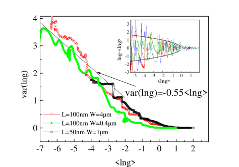
The explanation of this striking result lies in the very broad distribution of conductances in the dielectric regime. Theories of log-normal distributions of conductances [12] indicate that an anomalously large conductance, a rare event, dominates the total conductance. This is only valid at very low temperature, when parallel thermally activated conducting channels are exponentially small. According to the scaling theory of localization, at the metal-insulator transition, this event is the last conducting channel with conductance [13]. In samples consisting of many squares in parallel and since the conductance distribution is log-normal, this last conducting channel carries almost the total current.
Deep in the insulating regime, we find that the conductance fluctuations obey roughly to: , independent of geometry for widths up to [14] (see Fig. 2). Here is the variance of the average conductance where the average is taken over . The proportionality between the variance and the mean of is expected in disordered insulators at zero temperature and described by non-interacting scaling models[15]. However, since interactions are crucial to explain the details of the fluctuations as shown below, our experiment suggests that a one-parameter description of the metal-insulator transition (at least in the strongly insulating phase) holds even in the presence of interactions.
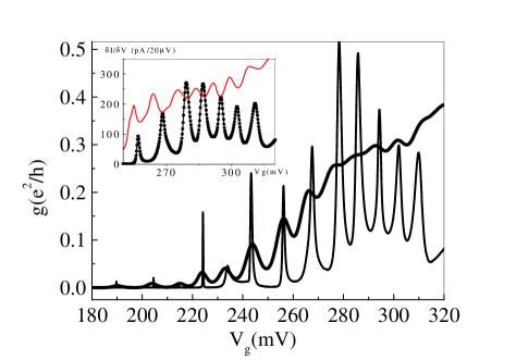
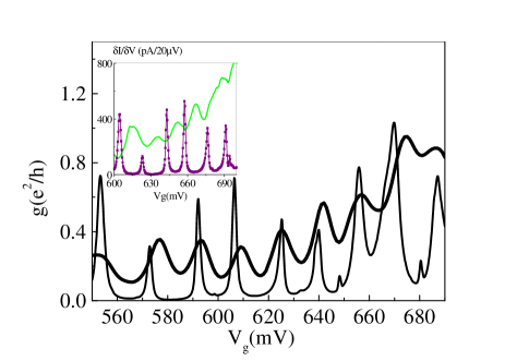
Fig. 3 shows Coulomb oscillations in our shortest samples with effective source drain distances of 25nm and 75nm. In both samples each conductance peak at corresponds to one peak at the lowest temperature. No additional peaks appear upon cooling and we only observe small shifts in gate voltage. This is consistent with single dot resonances and rules out multiple dot tunnelling as previously reported in quasi-1D wires[2, 16]. Actually, several dots acting in parallel explain qualitatively the complicated pattern observed in samples with widths larger than typically .
We first consider the series of resonances at relatively high gate voltage when the dot is filled with several electrons. Taking a simple Coulomb blockade model periodic conductance resonances occur if the temperature is lower than the charging energy . At zero source-drain voltage and such that where is the number of electrons in the dot, charge is transfered; If on the other hand , resonances occur at such that . This is demonstrated in the insets of Fig. 3. We suppose here that the capacitances to source and drain are equal. Within this classical model, we find and for the 100 nm sample, and and for the 50 nm sample. The charging energy is and respectively for the 100nm and the 50nm sample. In the simplest model, , in agreement with the value deduced from the temperature dependence of the resonances (see inset of Fig. 1 ).
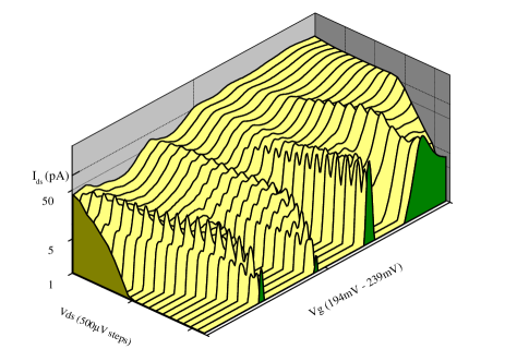
With decreasing number of electrons on the dot, the mean level spacing increases and the barrier resistance between source and drain and the impurity quantum dot increases. If the temperature is below the mean level spacing we can estimate by the non-linearities revealing the excited states of the dot. In our samples this is shown in Figure 4. Upon rising , the differential conductance exhibits a peak each time an excited state enters or exits the energy window . Up to 3 excited states ( 6 peaks in ) are distinguishable for resonances at low gate voltage for , such that . At higher gate voltage becomes smaller and the contrast between excited states is washed out (classical Coulomb blockade regime). Since is smaller but non negligible compared to , the periodicity of the Coulomb oscillations is not strictly obeyed.
The values for the mean spacing and charging energy are typical for all the measured samples. corresponds to what is expected for single electron levels in a 2D box of taking into account the reduced density of states in the Lifshitz tail. Alternatively it corresponds also to a parabolic potential confinement of radius 50 nm, comparable to the source-drain distance, and heigth 10 meV, comparable to the Fermi energy at the MIT. The capacitance to gate (L=100nm) (resp. for L=50nm) corresponds to a 2D dot of size (resp. ).
A main feature of our samples is the very thin gate oxyde which makes the gate very efficient to screen the Coulomb interaction in the IQD. For instance, a simple estimation of the repulsion between two bare electrons at a mean distance of in the channel gives where and are the relative dielectric constants of and . Since the oxyde thickness () is much smaller than the distance between two electrons, the Coulomb interaction is a dipole interaction.
The various above estimations confirm that the sequence of resonances reflects the interaction between electrons sharing the same (barely) localized site whose extension is comparable to the source-drain distance independent of the width of the channel or the dopand concentration. Furthermore, we have demonstrated in this way that in order to observe Coulomb blockade in nanostructures it is not necessary to constrict the current through a quasi 1D segment such as point contacts or wires. The domination of a rare event in a short 2DEG intrinsically favours a channel through a single IQD in not too wide geometries. In this way one has a better estimate of the relevant length and energyscales of the dot than in quasi 1D geometries. Also, downscaling the source-drain distance from 75nm to 25nm increases the Coulomb energy, as expected when the dot size of the charge transmitting IQD decreases with channel length.
In summary we have studied standard Si:MOSFETs of gate length and and various widths without any intentional confinement. Close to the MIT, characterized by at low temperature, conductance resonances as a function of the gate voltage are due to tunneling through a single disordered quantum dot, whose extension is comparable to the source-drain distance and which accomodates several electrons. In contrast to many previous studies on quasi-1d wires, our geometry allows to isolate single dot tunnelling in an impurity potential and quench multiple dot tunnelling. If the transverse dimension is increased too much, several IQD conduct for the same gate voltage ranges, causing eventually a complex structure of conductance resonances. Furthermore, we find that in the dielectric regime the variance of systematically scales with the average of . Such an observation is consistent with a one-parameter description of the metal-insulator transition. Finally, our results strongly suggest that reducing the channel length even further should imply the observation of Coulomb oscillations with a charging energy comparable to room temperature.
REFERENCES
- [1] J.H.F. Scott-Thomas et al. Phys. Rev. Lett. 62, 583 (1989).
- [2] C. deGraaf et al. Phys. Rev. B 44, 9072 (1991); A. A. M. Staring et al. Phys. Rev. B 45, 9222 (1992).
- [3] J.T. Nicholls et al. Phys. Rev. B 48, 8866 (1993).
- [4] L. Zhuang, L. Guo and S. Y. Chou, Appl. Phys. Lett. 72, 1205 (1998).
- [5] H. Ishikuro and T. Hiramoto, Appl. Phys. Lett. 71, 3691 (1997).
- [6] V. V. Kuznetsov et al. Phys. Rev. B 56, R15533 (1997); V. V. Kuznetsov et al. Phys. Rev. B 54, 1502 (1996); A.K. Savchenko et al. Phys. Rev. B 52, R17021 (1995).
- [7] D. Ephron et al. Phys. Rev. B 49, 2989 (1994).
- [8] A. B. Zorin, Rev. Sci. Instrum. 66, 4296 (1995).
- [9] The total carrier density is fixed by the threshold voltage, i.e. the gate voltage at which the inversion 2D layer is induced. It is estimated to be around zero volt for the 100 nm series ( +0.4V for the 50nm series).
- [10] M. Azbel Phys. Rev. B 28, 4106 (1983).
- [11] A very small background ( at ) has been added to the fit.
- [12] M. E. Raikh and I. M. Ruzin Sov. Phys. JETP 68, 642 (1989); F. Ladieu and J.P. Bouchaud, J. Phys. 1 France 3, 2311 (1993). F. Bardou Europhys. Lett. 39, 239 (1997).
- [13] Y. Imry Europhys. Lett. 1, 249 (1986).
- [14] For too wide samples, as well as for too long wires, . see W. Poirier, D. Mailly and M. Sanquer, Phys. Rev. B 59, 10856 (1999). The prefactor 0.55 is smaller than expected (1) perhaps due to the finite temperature.
- [15] J.L. Pichard and M. Sanquer in ”Quantum chaos”, G. Casati and B. Chirikov editors, Cambridge University Press 1995. J.L. Pichard and M. Sanquer, Physica A 167, 66 (1990).
- [16] I.M. Ruzin et al. Phys. Rev. B 45, 13469 (1992).