Dynamic electromagnetic response of three-dimensional Josephson junction arrays
Abstract
We present a theoretical study on the dynamical properties of three-dimensional arrays of Josephson junctions. Our results indicate that such superconducting networks represent highly sensitive 3D-SQUIDs having some major advantages in comparison with conventional planar SQUIDs. The voltage response function of 3D-SQUIDs is directly related to the vector-character of external electromagnetic fields. The theory developed here allows the three-dimensional reconstruction of a detected external field including phase information about the field variables. Applications include the design of novel magnetometers, gradiometers and particle detectors.
I. Introduction
Oscillators based on arrays of Josephson junctions operating in the voltage mode have shown to be promising radiation sources in the mm- and sub-mm wavelength range. One of the most remarkable features of such systems is that the microwave power output increases with the number of array junctions while at the same time the linewidth of the generated high-frequency voltage oscillation decreases with this number [6]. The latter phenomena is not only interesting for the application of the arrays as microwave sources but also for their application as highly sensitive detectors. From this point of view, two- and three-dimensional arrays of Josephson junctions represent multi-junction interferometers which can be used e.g., as magnetometers, gradiometers or particle detectors.
The capabilities of 2D- and 3D-Josephson arrays can be used successfully if all array junctions operate in a coherent array mode, i.e., if they oscillate strongly phase-locked [3,6]. The problem of phase-locking in 2D-arrays is presently subject of intensive research and great experimental and theoretical progress has been achieved using present-day integrated-circuit technology [1-3]. Since this technology is essentially two-dimensional there are up to now no corresponding experimental and theoretical studies on 3D-arrays. However, 3D-arrays of Josephson junctions may be promising candidates for highly sensitive detectors which allow as a new quality the three-dimensional reconstruction of the detected electromagnetic field including phase information about the field variables. In view of recent developments in molecular beam epitaxy the fabrication of 3D-arrays with appropriate junction parameters and array homogeneity seems to be possible in the nearest future.

In this paper we present theoretical results on the dynamical properties of a 3D-system of coupled Josephson junctions. A schematic drawing of the 3D-network is shown in Fig.1. It consists of superconducting islands (large cubes) connected by Josephson junctions (smaller dashed cubes). This system is the simplest three-dimensional configuration that guarantees coherent operation, i.e., single frequency operation, if it is DC biased parallel to one of the networks’ axes (c.f. Fig.2). If in the voltage state of the array a magnetic field is applied to the network, the six intrinsically coupled four-junction DC SQUIDs lying on the six faces of the cube are generating field dependent macroscopic current and voltage distributions which can be easily measured. From the AC Josephson effect and the flux quantization condition the current and voltage distributions depend directly but nonlinearly on the strength and the orientation of the external field.
II. Network equations
To get quantitative results about the networks’ response function we will consider a network built by junctions which can be described by the RCSJ-model, e.g., externally shunted junctions. However, if other SIS-type junctions are used the results remain qualitatively valid. Fig.2 shows the equivalent circuit for the 3D-network which is DC biased along the x-direction. It consists of Josephson junctions (crosses) which are connected by superconducting wires. The bias current is fed into and extracted from the network through ohmic resistors (which must not necessarily be equal). This method of biasing preserves well defined boundary conditions for the networks dynamics and removes some of the ambiguities due to the symmetry of the system. Since the bias current is flowing parallel to the x-axis there are two groups of junctions with different dynamical behavior. The junctions lying parallel to the bias current (active junctions) switch into their voltage state for , where is the critical current of the array depending on the externally applied flux . The junctions lying perpendicular to the bias current (passive junctions) do in general not switch into the voltage state but show librations (semirotations) of their Josephson-phase differences. The amplitude of these librations is directly related to the strength and orientation of the external field. If the values of the ohmic resistors at the current in- and output do not differ too much, the passive junctions are in the zero-voltage state and the only frequency present in the system is the driving frequency defined by the active network junctions. This prevents chaotic or aperiodic dynamics of the junction phases.

In the temporal gauge the variables characterizing the dynamics of the junction network are the gauge invariant phase differences [4,5]. If we denote the vector of the 12 network variables by and use the usual reduced units [1] the system of coupled network equations can be written symbolically as
where is the magnetic penetration depth, the inductance matrix of the array, the matrix of the distribution of the external flux over the different network meshes and the matrix which describes the distribution of the currents induced by the oscillating electric field vector of an incoming external wave. The elements of and depend on the orientation of the external electromagnetic field. and are the matrices which define the boundary conditions depending on the values of the eight input and output resistors The single junction parameters are the McCumber parameter , the critical current and the normal resistance . is the magnetic flux quantum and the lattice spacing measuring the distance between the centers of adjacent superconducting islands. The inductance matrix includes all inductances present in the array and depends on the geometry of the network and the inductances of the single junctions. We determine the coefficients of by assuming an array geometry similar to that shown in Fig.1 and by using junction inductances which are typical for externally shunted junctions. Changing the geometry of the network or the value of the junction inductances, however, influences our results only slightly.
The network equation (II.) clearly shows the dependence of the time evolution of the network phases on the applied quasi-static external magnetic field which can approximately be expressed as , where is the magnetic field vector of the external field. The sensitivity of the network depends on the lattice spacing and reaches its maximum for vanishing magnetic coupling within the network, i.e., for infinite magnetic penetration depth For , however, the network response vanishes totally. The sensitivity of the network dynamics with respect to distinct directions of the magnetic field, i.e., the anisotropy of the response function, can be manipulated by an appropriate choice of the input and output resistors.
The device possesses in principle two modes of operation. The DC mode with and the AC mode with . For subcritical bias currents , a constant external field induces constant loop currents in the meshes of the network and the resulting current distribution within the array is a superposition of these loop currents with the bias current. The critical array current is a function of the strength of the external field and the orientation of this field. However, because of the many degrees of freedom of the system the response function is not unique. There exists in general for any given a whole set of different equilibrium current distributions in the network on which the critical array current depends [5,7]. By a detailed theoretical analysis it is possible to formulate selection rules which describe the external field depending transitions between the different distributions. Although there occur in the region of subcritical bias currents very interesting dynamical phenomena, the scenario becomes very complicated and will be presented elsewhere [7].
In the following we will restrict our treatment to the AC mode of the network. For the active array junctions show persistent voltage oscillations whose frequency is directly proportional to the voltage drop. If the constant voltage drop originating from the input and output resistors is subtracted, the averaged voltage drop across the array is for given by , where the summation runs over the four active network junctions lying parallel to the x-axis and denotes time averaging over one oscillation period. Due to flux quantization, the network currents induced by the external field are converted by the network dynamics into oscillating loop currents in each network mesh. The voltage oscillation induced by these oscillating loop currents interferes with the voltage oscillation of the active junctions, so that the averaged voltage drop across the whole array becomes a function of the strength and the orientation of the external field.
III. Results
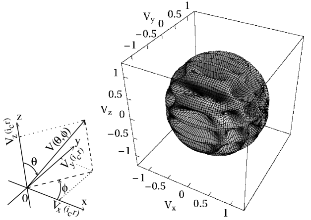
By numerically integrating the network equation (II.) we computed the macroscopic voltage response function of the 3D-network for various different sets of junction and array parameters. In the following we present typical results. Fig.3 shows a spherical plot of the voltage response function for , and a homogeneous magnetic field which induces a flux Here is a vector with unit length pointing in the direction given by the spherical coordinates and and the origin is put in the center of the 3D-array (c.f. Fig.3). The voltage response function is plotted in the form , where is the macroscopic averaged voltage drop across the array measured in units of . The eight input and output resistors (c.f. Fig.2) all have the same value so that, corresponding to the symmetry of the network, the voltage response function shows a periodicity with period along each closed intersection curve with the x-z-, x-y- and y-x-plane, respectively, and a reflection symmetry with respect to each integer multiple of
In Fig.4(a) intersection curves in the z-y-plane, i.e., , are plotted for and different values of . The symmetry of the voltage response functions with respect to integer multiples of is clearly observable and the sensitivity of the network reaches its maximum around integer multiples of For such values of the field vector of the external magnetic field lies directly perpendicular to one of the faces of the cube and the induced currents in general become maximal in the direction parallel (and antiparallel) to the bias current. In this case the externally induced voltage drop becomes also maximal. The number of local maxima and minima of the voltage response function is strongly related to the applied flux and can be determined numerically.
| (a) |

|
| (b) |

|
The resolving power of 3D-SQUIDs with respect to the strength of external magnetic fields is comparable to the resolving power of a conventional 2D-SQUID, i.e. a SQUID loop with two junctions. The angular resolution of 3D-SQUIDs, however, is orders of magnitudes better than for 2D-SQUIDs. For external magnetic fields inducing a flux in the order of one, the transfer factor lies around which is for typical junctions in the range of some V, such that, e.g., an angle of should be easily resolvable. The resolving power with respect to the strength and the resolving power with respect to the direction of an external field can be further increased by using networks which consist of several cubes. In this case the resolution powers increase proportional to the number of cubes.
Fig.4(b) shows for comparison the angular resolution of the 3D-junction array and a corresponding conventional 2D-SQUID. Both configurations are considered to have identical parameters. If the applied magnetic field lies perpendicular to the 2D-SQUID plane, i.e. , the device is very insensitive to variations of . This insensitivity, however, has advantages if only the strength of the magnetic field is to be measured. In contrast to this, the 3D-array’s response is very sensitive to variations of the direction of the external magnetic field. Therefore, the 3D-network has the advantage that simultaneously the strength and the direction of the magnetic field can be measured very precisely.
Three-axis SQUIDs, which consist of three independent operating 2D-SQUIDs are not directly comparable with 3D-SQUIDs. For three-axis SQUIDs the three independent voltage response functions are computationally postprocessed and the information about strength and orientation of the magnetic field vector is computationally extracted. In contrast to this, the single voltage response function of 3D-SQUIDs provides all information at once and no further postprocessing is needed.
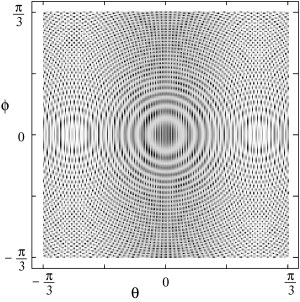
For increasing the number of local maxima and minima of the voltage response function grows. Fig.5 shows density plots of the response function for a solid angle with , and (a) and (b) . The network parameters are the same as for Figs.(3) and (4). The minima (black dots) and maxima (white areas) form significant patterns which are quite similar to optical interference patterns. However, according to Eq.(II.) these patterns are a result of nonlinear interactions and a trace of their nonlinear origin are the complex local structures occurring in Fig.5(b). By evaluating the voltage response patterns, the strength of the external magnetic field and, up to the symmetry redundancy, the orientation of this field can be determined very precisely. The symmetry redundancy can be removed by an appropriate choice of the input and output resistors. In this case, however, the resistors possess slightly different values and the voltage response of the network becomes much more complicated and more difficult to interpret [7].
| (a) | (b) |
|---|---|
|

|
If the parameters of the array junctions and the dimension of the 3D-network are chosen appropriately, the systems are also able to detect time dependent electromagnetic fields with wavelengths which lie typically in the mm-range. For time dependent external fields the induced flux becomes time dependent and the currents are induced by the oscillating electric field vector of the external wave (c.f. Eq.1). In contrast to 2D-configurations, for which the influence of the oscillating magnetic field is in general negligible, for the 3D-network both field vectors contribute to the response function of the array if the lattice spacing is chosen appropriately. Fig.6 shows current-voltage characteristics of the 3D-network for different fixed directions of the external microwave and array parameters and . The microwave is assumed to be linearly polarized parallel to the bias current and the amplitudes of the externally induced flux and of the induced current are . The frequency of the external microwave is in Fig.6(a) and in Fig.6(b), and is the normalized bias current. In each of both figures the I-V-curves for the magnetic field directions (solid curve) and (dashed curve) are plotted, and, for comparison, the I-V-curve for negligible influence of the magnetic field (dotted curve).
| (a) |

|
| (b) |

|
It is clearly observable that the I-V-characteristics depends on the direction of the incoming wave and that the magnetic part is indeed relevant. In general, the distribution of the Shapiro steps and their width differ significantly from those corresponding to a single junction. In addition, it can be observed that for some characteristics the step plateaus show an unusual fine structure. The first, fifth and seventh step on the left characteristics in Fig.6(a) show such structures. These fine structures are according to Eq.(1) implied by the different contributions of the electric and the magnetic field to the network dynamics. We observed that on the Shapiro steps the network junctions first lock to the electric part of the external microwave and then for increasing bias current eventually also to the magnetic part. This can change the current distributions within the network and implies a slight decrease in the averaged voltage drop and therefore in the network frequency.
The 3D-network dynamics governed by Eq.(1) includes all informations about the field variables of the external microwave. By a detailed analysis it is therefore possible to extract from the macroscopic current and voltage response functions of the network the information about the phase relationship within the incoming wave.
By assuming the simple model of a circularly polarized incoming microwave we can show that the voltage response function of the 3D-network is directly affected by the helicity of the external field. The inset of Fig.6(b) shows the I-V-characteristics near the critical array current for for a microwave that is linearly polarized in the x-direction (solid curve) and a microwave that is circularly polarized in the z-x-plane (dashed curve). The splitting between the critical array current of the two modes lies in the range of several and the shape of the characteristics differ significantly. This result already indicates that the 3D-network can operate phase-sensitively and that the modulations in the voltage response function caused by differently polarized external microwaves should be easily observable in experiments.
IV. Conclusions
By presenting various theoretical results we have shown that 3D-networks of Josephson junctions represent ultrasensitive 3D-SQUIDs which can be useful for a number of different applications like magnetic field sensors, video detectors or mixers. Especially the capability of the networks to operate direction-sensitively and to detect incoming microwaves phase-sensitively is a novel quality and may allow the design of a new generation of superconducting devices.
Acknowledgment
Financial support by the Forschungsschwerpunktprogramm des Landes Baden-Württemberg is gratefully acknowledged.
References
- [1] K. Wiesenfeld, S.P.Benz and P.A.A. Booi, J. Appl. Phys. 76, 3835 (1994).
- [2] A.B. Cawthorne, P. Barbera and C.J. Lobb, IEEE Trans. Appl. Supercon. 7, 3403 (1997).
- [3] J. Oppenländer, W. Güttinger, T. Traeuble, M. Keck, T. Doderer, and R.P. Huebener, “Two-dimensional Josephson junction network architectures for maximum microwave radiation emission” to appear in IEEE Trans. Appl. Supercon. (1999).
- [4] D. Dominguez and J.V. José, Phys. Rev. B 53, 11692 (1996).
- [5] R. De Luca, S. Pace, C. Auletta, and G. Raiconi, Phys. Rev. B 52, 7474 (1995); R. De Luca, T. Di Matteo, A. Tuohimaa, and J. Paasi, Phys. Rev. B 57, 1173 (1998).
- [6] K.K. Likharev, Dynamics of Josephson junctions and circuits. Gordon and Breach, New York, 1991.
- [7] J. Oppenländer, Ch. Häussler and N. Schopohl, ”Interaction of a cubic Josephson junction network with external electromagnetic fields”, to be published.