Anomalous behaviour of S/N mesoscopic structures near .
Abstract
We observe a maximum in the conductance of Aluminum / n-GaAs junctions at temperatures 20 mK lower than the superconducting transition temperature. This is the first observation of a peak in the conductance near the superconducting transition in superconducting normal junctions. To accommodate this effect we calculate the full temperature dependence of the conductance of these structures, invoking quasiclassical Green’s functions in the diffusive limit. In addition to the well-known low temperature peak at temperatures on the order of the Thouless energy, we find a maximum near the critical temperature. This peak has the same origin as the subgap conductance observed in superconducting-normal junctions at low temperatures. Its calculated magnitude and position are in reasonable agreement with our experimental observation.
Pacs numbers: 72.10.Fk, 72.15.Gd
The study of transport properties of mesoscopic normal superconducting (N/S) structures has revealed a number of novel features [1, 2], including long-range, phase-coherent transport, disorder-enhanced subgap conductance [3] and a non-monotononic dependence of the conductance on temperature () and voltage (). Such a non-monotonic dependence was first predicted in [4] for a short point N/S contact of length satisfying, where is the diffusion coefficient and is the energy gap of the superconductor at zero temperature. In Ref.[4] it was shown that , as a function of or , increases from ( is the conductance in the normal state) at and , reaches a maximum at or of order and then decreases to as or are increased further. In the opposite limit,
| (1) |
where is the Thouless energy, the conductance reaches a maximum when or when is of order [5, 6, 7, 8, 9]. These predictions have stimulated many experimental studies of the sub-gap conductance of S/N systems and this low temperature maximum has been observed in both short and long S/N structures [10, 11, 12, 13].
In Refs. [14, 15] it was predicted that besides the maximum , which is an energy scale distinct from , a new maximum in the conductance may appear near when is of order [16]. This new maximum arises from an interplay between the two hitherto decoupled energy scales, and . Thus one can probe both the energy gap in the superconductor and a pseudogap induced in the normal region, at an easily accessible (viz. high) temperature range. The pseudogap dependence on various parameters such as the magnetic field and Coulomb interaction can then be tested against theoretical predictions [17, 18, 19]. Until now however, this maximum has remained experimentally elusive.
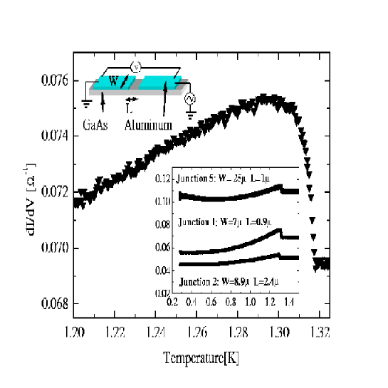
We present here the first experimental observation of a maximum in the conductance of S/N and S/N/S structures in the vicinity of . The structures measured are of a coplanar geometry (Top Inset in Fig. 2; see also Fig.1(B)) in which the separation between the superconducting contacts is larger than the coherence length ( is the diffusivity) in the GaAs layer. Our results for this structure are applicable in particular to the limit described by Eq. (1), although the parameters and geometry are different than those used in [14, 15]. For the first time we identify a significant conductance maximum near , which occurs when is roughly equal to divided by the ratio of the Al/GaAs interface resistance to the resistance through a vertical portion of the conducting GaAs layer the thickness of which is .
The junctions were made of 200 nm Al deposited in-situ in a molecular beam epitaxy chamber, on heavily doped GaAs (the thickness of the heavily doped region is 150 nm) [20]. Conducting bars of width m were then patterned by an acid etch. Finally an aluminium strip of length m was removed by a second acid etch, thus defining the two contacts (Top left Inset of Figure ). The conductance was then measured via a standard four terminal low frequency (77Hz) ac lockin technique. The data presented in Fig.2 is the conductance of a junction patterned on a bar 7 microns wide with a contact separation of 0.9 microns. The sample is characterized by the following parameters [20]: the sheet resistances of the normal aluminium layer and the doped semiconducting layer (at ) are 0.02 and 90 per square respectively. The interface Al/GaAs-n resistance is cm2, the average carrier density in GaAs-n is 3.610 cm-3 (it varies in that layer between 310 - 510cm-3) yielding the diffusion coefficient cms. Thus the coherence length is 0.2(0.1) microns at T = 0.3(1.3) K, shorter than the contact separation.
As Fig.2 shows, at the superconducting transition, the conductance increases, reaching a maximum when the temperature is 20 mK colder than the point at which the conductance was first affected [21]. The trend is then reversed as the temperature is further decreased. Note that a decrease in the conductance (increase in the resistance) was earlier observed by Kleinsasser and Kastalsky [3] on the Nb/InGaAs structure. We have observed the effect in 9 samples including both S/N and S/N/S junctions with varying contact separations (mm) and the bar width (m). The magnitude of the conductance enhancement at the transition divided by the contact width is of the same magnitude for all samples, thus confirming that it is a property of one S/N junction.
To calculate the conductance variation of the structures shown in Fig. 1 (A,B). we assume the diffusive limit and exploit a quasiclassical Green’s function technique which has been well developed for studying transport in S/N structures (see Ref.[2] and references therein). The normalized conductance variation of the N’/N/S structure (N’ is the normal reserviour), , is given by (see Ref.[22]),
| (2) |
Here is the derivative of the distribution function in the N’ reservoir (we set the electric potential in S equal to zero), , are the ratios of the N’/N and N/S interface resistances to the resistance of the N layer. The denominator represents contributions to the total resistance at a given energy (or at a given voltage at zero temperature). The first term in the denominator describes the spatially averaged spectral resistance of the N layer, which is decreased due to the proximity effect. The second and third terms in the denominator are the N’/N and N/S interface spectral resistances. The terms and representing the DOS in the N layer and the S reservoir lead to an increase of the N’/N and N/S interface resistances. The function represents a factor contributing to the subgap conductance, which may lead to a decrease of the S/N interface resistance. All the functions in Eq. (2) are expressed in terms of the retarded Green’s functions and in the N film as
| (3) |
In order to calculate the conductance variation given by Eq.(2), we need to find the Green’s functions and . These functions obey the Usadel equation which after parametrization , acquires the form,
| (4) |
where . Eq. (4) is complemented by boundary conditions (see for example [2]).
Eq. (4) can be solved analytically in two cases. The simplest case corresponds to a weak proximity effect when the Usadel equation can be linearised. This can be done if the condition is satisfied. The second case corresponds to a short structure [14]. We are interested in energies of the order (see below) which are much smaller than the critical temperature Hence the relevant length scale in Eq.(4) is longer than the characteristic length for the Josephson effect . In a short contact (that is, ), the solution of Eq. (4) is almost uniform along the layer for energies of order , and has the form [14],
| (5) |
where , , is the damping in the energy spectrum of the superconductor S, and is the Thouless energy. This solution is valid provided that the conditions, are fulfilled.
With the help of the functions , one can easily calculate all the functions in the expression for the conductance using Eq.( 2). In calculating the conductance with the help of Eq.(2), we used both analytical and numerical solutions of the Usadel equation, Eq. (4). We calculate the temperature dependence of the conductance for both types of structures shown in Fig.1. Our results show that the maximum near is not a specific characteristic of a coplanar geometry (Fig.1(B)), but is present in both cases and related to a contribution of the subgap current to the conductance. It is worth also mentioning that the position and amplitude of the maximum do not depend essentialy on the length of the structure (unless the Josephson effect becomes important in a S/N/S structure). We distinguish the cases of long and short contacts in order to make the theoretical analysis more transparent.
First we consider the structure shown in Fig1(A). It turns out that the solution of the linearised Eq. (4) is a good approximation even in the case of comparable interface and N film resistances ( and are of order 1). In Fig. 3 we plot the temperature dependence of the normalised conductance variation for a long S/N/S structure shown in Fig. 1(A) (here is the conductance of the system in the normal state). As is seen from Fig. 3, a small maximum in appears at a temperature which is very close to and corresponds to the value of comparable with the Thouless energy . With decreasing temperature the conductance variation decreases and becomes negative as it should be if the interface resistance exceeds the resistance of the N layer.
Using Eq.(5), we calculate the temperature dependence of the conductance for the short structure shown in Fig. 1(A) for different values of parameters and show this dependence in Fig.4 (two lower curves). As in the previous case of a long structure there is a small maximum near . In this case the position of the maximum corresponds to equal approximately to the energy at which the DOS in the N layer has a maximum and below which the subgap conductance ( term in Eq.(2)) is enhanced. With decreasing temperature the conductance variation decreases and becomes negative. The conductance variation may have a minimum and a second maximum at lower temperatures (subgap conductance). Preliminary measurements carried out at low temperatures reveal a minimum in the conductance in the temperature range 70 mK in qualitative agreement with the theory. Analysing the energy dependence of different functions in the intergrand of Eq.(2), one can see that both the low temperature maximum and the maximum near are caused by a contribution of the term which describes the subgap charge transfer through the S/N interface via Andreev reflection processes.
Consider now the coplanar structure (see Fig.1 (B)). One can show that in this case the conductance variation is determined again by Eq.(2) with replaced by and replaced by (here is the sheet resistance of the semiconducting layer). In the case of a short structure () all the functions in the expression for ( etc) are constant in space and given by Eq. (5) with replaced by . This means that in a coplanar structure plays the role of an effective Thouless energy. Therefore the position of the maximum depends on weakly and is determined by the pseudogap induced in the N layer beneath the superconducting electrode.
In Fig.4 we present the temperature dependence of the conductance variation near for the coplanar structure with parameters close to the experimental ones. One can again see that there is a maximum near at a temperature corresponding to .
The presented theoretical results qualitatively fit the experimental data and give a reasonable quantitative agreement. The normalized value of the peak observed experimentally is about 10% and its position with respect to the critical temperature is Theoretical values of vary from tenth of percents (weak proximity effect) to 10% (strong proximity effect) and values of vary from to . Estimations of characteristic parameters for a coplanar structure give for and the approximate values 0.2-5, 5-10 and 5 K respectively. Therefore the theoretical values for and are in reasonable agreement with experimental data taking into account approximations made in the course of calculations (for example, in case of S/N/S junctions, we neglect the Josephson effect which seems to be suppressed by thermal fluctuations) and uncertainties in the experimental value for the S/N interface resistance.
To summarise, we have for the first time observed a maximum in the conductance of mesoscopic diffusive S/N, S/N/S structures in close vicinity of the critical temperature. The maximum is caused by the contribution of Andreev reflection processes to the pseudogap conductance of the S/N interface. These processes are the ones which lead to the subgap conductance at low temperatures. Our calculation shows that the conductance will peak when the superconducting gap is of order of the subgap which is in reasonable agreement with the experimental observation. Studies of this maximum provide a new way to probe the effect of the Coulomb interactions on the induced subgap in the semiconducting region. The theory and experimental data presented here show that the maximum in the conductance near is not related to non-stationary Josephson effects.
We are grateful to D.E.Khmelnitskii, B.D.Simons and D. Taras-Semchuk for discussions and encouragement at the initial part of the work and to V. Pavlovksii for help in numerical calculations. We are grateful to the Royal Society, the EPSRC and to the Isaac Newton Trust for their financial support.
REFERENCES
- [1] C.W.J.Beenakker, Rev.Mod.Phys. 69, 731 (1997).
- [2] C.J. Lambert and R.Raimondi, J. Phys. Cond. Matter, 10,5,901 (1997)
- [3] A.Kastalsky et al., Phys. Rev. Lett., 67,1326 (1991); A.W.Kleinsasser and A.Kastalsky, Phys.Rev. B47, 8361 (1993)
- [4] S.N. Artemenko, A.F. Volkov, and A.V. Zaitsev, Solid State Comm. 30, 771 (1979)
- [5] Yu.V. Nazarov and T.H. Stoof, Phys. Rev. Lett. 76,823 (1996)
- [6] S.Yip, Phys. Rev. B52, 15504(1995)
- [7] A.F. Volkov, N. Allsopp, and C.J. Lambert, J. Phys. Cond. Matter 8, 45(1996).
- [8] A.A.Golubov, F.Wilhelm, and A.D.Zaikin, Phys.Rev. B55, 1123 (1996).
- [9] A.F. Volkov and V.V. Pavlovskii, in Correlated Fermions and Transport in Mesoscopic Systems, ed by T. Martin, G. Montambaux and J. Tran Thanh Van, Frontiers, Gif-sur-Yvette Cedex,France,1996
- [10] V. N. Gubankov and N. M. Margolin, JETP Letters 29, 673 (1979)
- [11] H. Courtois, Ph. Grandit, D. Mailly, and B. Pannetier, Phys. Rev. Lett. 76, 130 (1996); D. Charlat, H. Courtais, Ph. Grandit, D. Mailly, A.F. Volkov, and B. Pannetier, Phys. Rev. Lett. 77, 4950 (1996).
- [12] S.G.Hartog et al., Phys. Rev. B56, 13738 (1997).
- [13] V.T. Petrashov, R. Sh. Shaikadarov, P. Delsing, and T. Claeson, Pis’ma v ZhETF 67, 489 (1998)
- [14] A.V.Zaitsev, Pis’ma Zh.Exp.Teor.Fiz. 51, 35 (1990) [JETP Letters, 51, 41 (1990)].
- [15] R. Seviour, C. J. Lambert, and A. F. Volkov, Phys.Rev. B59, (9) (1999);J. Phys. Cond. Matter 10 , L615 (1998)
- [16] Strictly speaking, the position of this maximum, as we will see, depends also on the interface resistance which makes an effective Thouless energy smaller.
- [17] A.Huck, F.W.J.Hekking and B.Kramer, Europhys.Lett. 41, 201 (1998)
- [18] A.Atland, B.D.Simons and D.Taras-Semchuk, cond-mat/9807371
- [19] M.Feigelman, A.I.Larkin and M.A.Skvortsov, cond-mat/9907358
- [20] The parameters for the Al (heavily doped GaAs) were obtained by measuring the conductance of the samples where the Al layer was left fully intact (fully removed). The Al/GaAs interface resistance was measured using the standard differential model by comparing the overall junction resistance to the resistance of the semiconducting portion with the junction length.. The number given is the average measured from 7 SNS junctions in the normal state. Further details will be published elsewhere; for the Al-GaAs see also R. Taboryski, T. Clausen, J. Bindslev Hansen, and J. L. Skov, J. Kutchinsky, C. B. Sorensen, and P. E. Lindelof, Applied Physics Letters 69, 656 (1996)
- [21] A portion of the conductance enhancement upon ( for the various samples) is due to the vanishing resistance of the aluminium layer between the voltage probes. In junction 1 (figure 3) of the conductance enhancment () upon the transition is due to this effect.
- [22] A.F.Volkov, A.V.Zaitsev and T.M.Klapwijk, Physica C210, 21(1993)