Conductance of Distorted Carbon Nanotubes
Abstract
We have calculated the effects of structural distortions of armchair carbon
nanotubes on their electrical transport properties. We found that the bending
of the nanotubes decreases their transmission function in certain energy
ranges and leads to an increased electrical resistance. Electronic structure
calculations show that these energy ranges contain localized states with
significant - hybridization resulting from the increased
curvature produced by bending. Our calculations of the contact resistance
show that the large contact resistances observed for SWNTs are likely due to
the weak coupling of the NT to the metal in side bonded NT-metal
configurations.
Carbon nanotubes (NTs) can be metallic or semiconducting. They have high
mechanical strength and good thermal conductivity [1],
properties that make them potential building blocks of a new, carbon-based,
nanoelectronic technology [2, 3, 4, 5]. Conduction in
defect-free NTs, especially at low temperatures, can be ballistic, thus
involving little energy dissipation within the NT [6]. Furthermore,
NTs are expected to behave like quasi one-dimensional systems (Q1D) with
quantized electrical resistance, which, for metallic armchair nanotubes at
low bias should be about 6 k (). The experimentally observed
behavior is, however, quite different. The contact resistance of single-wall
nanotubes (SWNTs) with metal electrodes is generally quite high.
Furthermore, at low temperatures a localization of the
wavefunction in the nanotube segment contained between the metal electrodes
is observed that leads to Coulomb blockade phenomena [7]. The
latter observation suggests that a barrier or bad-gap develops along the NT
near its contact with the metal. In an effort to understand the origin of
these discrepancies we have used Green’s function techniques to calculate the
effect of the modification of the NTs by bending on their electronic structure
and electric transport properties. We also investigated the effects
of the strength of the NT-metal pad interaction on the value of the contact
resistance.
Most discussions on the electronic structure of NTs assume perfect
cylindrical symmetry. The introduction of point defects such as vacancies
[8] or disorder [6, 9] has been shown to lead to
significant modification of their electrical properties. Here we focus on the
effects of structural (axial) distortions on the transport properties of
armchair NTs. AFM experiments [10] and molecular mechanics
simulations [11] have shown that the van der Waals forces between
NTs and the substrate on which they are placed can lead to a significant
deformation of their structure. To maximize their adhesion energy the NTs
tend to follow the topography of the substrate [10, 11]. Thus,
for example, NTs bend to follow the curvature of the metal electrodes on
which they are deposited. When the strain due to bending exceeds a certain
limit, kinks develop in the nanotube structure [10, 12, 13].
It is important to understand how these NT deformations affect the electrical
transport properties of the NTs. Could they be responsible for the low
temperature localization observed ? [7] Early theoretical work
on this issue was based on tight-binding model involving only the
-electrons of the NTs and accounted for the electronic structure changes
induced by bending through the changes in -orbital overlap at neighboring
sites. This study concluded that bending distortions would have a negligible
effect on the electrical properties of the NTs [14]. The
applicability of this approach is limited to weak distortions. Experiments,
however, show that strong deformations and kink formation are common. Under
such conditions, bending-induced - mixing, which was not
considered before, becomes very important in strongly bent NTs
[15]. In this work, the NT electronic structure is computed
using the extended Hückel method (EHM) [17] that includes both
and valence electrons. We have previously [16] shown
that EHM calculations on an armchair NT model (96 Å long)
reproduce the electronic properties obtained with more sophisticated ab-initio and band structure computations on NTs.
The approach we used in the computation
of the electrical properties is similar to that of Datta et al.
[18, 19].
The conductance through a molecule or an NT cannot be easily computed; even
if the electronic structure of the free molecule or NT is known, the effect
of the contacts on it can be substantial [20] and needs to be taken
into account. Typically, there will be two (or more) leads connected to the
NT. We model the measurement system as shown in Figure 1a. The leads are
macroscopic gold pads that are coupled to the ends of the NT through matrix
elements between the Au surface atoms and the end carbon atoms of the NT. In
most experiments to date the NTs are laid on top of the metal pads. As we
discussed above, the NTs then tend to bend around the pads. Such bending
deformations are modelled in our calculations by introducing a single bend
placed at the center of the tube.
The electrical transport properties of a system can be described in terms of the retarded Green’s function [18, 21]. To evaluate the conductance of the NT we need to compute the transmission function, , from one contact to the other. This can be done following the Landauer-Büttiker formalism as described in [18]. The key element of this approach lies in the treatment of the infinite leads which are here described by self-energies. We can write the Green’s function in the form of block matrices separating explicitly the molecular Hamiltonian. After some simplification we obtain:
| (1) |
where and are the overlap and the Hamiltonian matrices, respectively, and are self-energy terms that describe the effect of the leads. They have the form with the Green’s function of the individual leads [19, 22] and is a matrix describing the interaction between the NT and the leads. The Hamiltonian and overlap matrices are determined using EHM for the system Gold-NT-Gold. The transmission function, , that is obtained from this Green’s function is given by [18]:
| (2) |
In this formula, the matrices have the form:
| (3) |
The summation over all conduction channels in the molecule allows the evaluation of the resistance at the Fermi energy, . Transport in the presence of an applied potential is also computed. The differential conductance is computed in this case using the approximation [18]:
| (4) |
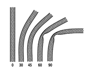
with describing the equilibration of the nanotube energy levels with respect to the reservoirs [19]. As a reference, we use the obtained from EHM for individual nanotubes as the zero of energy. The NT model used in our calculations is a carbon nanotube segment containing 948 carbon atoms. The bond distance between carbon atoms in non-deformed regions of the NT is fixed to that in graphite 1.42 Å, leading to a tube length of 96 Å. The building of deformed NTs using molecular mechanics minimization schemes [23, 24] has been described in detail elsewhere [15]. The structures of the bent NTs are shown in Figure 1b. The metallic contacts consist each of 22 gold atoms in a (111) crystalline arrangement. The height of the NT over the gold layer is 1.0 Å, where the Au-C bond distances vary from 1.1 to 1.6 Å.
a

b
In Figure 2 we present the computed transmission function for the bent
tubes (note that represents the sum of the transmission probabilities
over all contributing NT conduction channels). The upper-right of Figure 2
shows the raw transmission results obtained for the straight NT. The fast
oscillations of are due to the discrete energy levels of the finite
segment of the carbon nanotubes used. For clarity, we will use smoothed curves in
the description of the results. At , is about 1.2, leading to a
resistance ( 11 k ) higher than expected for ballistic
transport ( 6 k for = 2.0). This reduction in
transmission is due to the contribution from the contact resistance.
The increasing at higher binding energies is due to the
opening of new conduction channels. The asymmmetry in the transmission T(E) is
a function of the NT-pad coupling (C-Au distance). A longer NT-Au distance
increases the T(E) above , while it decreases it below , and vise
versa. Since the NT-pad geometry is kept fixed in all computations, this
behavior does not influence the effects induced by NT bending.
According to our calculation the contact resistance at is only about 5 k, much smaller than the 1 M resistance typically observed in experiments on single-wall NTs [2, 5]. The dependence of and contact resistance at on the Au-NT distance is shown in the upper-left of Figure 2. We see that remains nearly constant between 1-2 Å, then decreases exponentially. For distances appropriate for van der Waals bonding ( Å) the contact resistance is already in the M range. The above findings suggest that the high NT contact resistance observed experimentally may, in addition to experimental factors such as the presence of asperities at the metal-NT interface, be due to the topology of the contact. In most experiments, the NT is laid on top of the metal pad. The NT is at nearly the van der Waals distance away from the metal surface, and given that transport in the NT involves high -states which decay rapidly perpendicular to the tube axis, the coupling between NT and metal is expected to be weak [25]. Direct chemical bonding between metal and the NT, or interaction of the metal with the NT cap states [26] should lead to stronger coupling. In this respect, it has been found [27] that high energy electron irradiation of the contacts leads to a drastic reduction of the resistance. Since the irradiation is capable of breaking NT C-C bonds it may be that the resulting dangling bonds lead to a stronger metal-NT coupling.
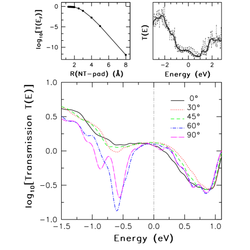
The strongest modification of as a result of bending is observed at around =-0.6 eV where a transmission dip appears. This dip is strongest in the bent NT. Furthermore, its transmission function at higher binding energies (BE) is lower than those of the 0∘-45∘ bent NTs, indicating that the transmission of higher conduction channels is also decreased. The nature of the dip at about -0.6 eV can be understood by examining the local density-of-states (LDOS) of bent tubes shown in Figure 3 [15]. A change (increase) in the LDOS is seen in the same energy region (0.5-0.8 eV below ) as the transmission dip. This change is essentially localized in the vicinity of the deformed region. The new states result from the mixing of and levels, have a more localized character than pure states leading to a reduction of . As Figure 3 shows, the change in transmission with bending angle is not gradual; the transmission of the 30∘ and 45∘ models is only slightly different from that of the straight tube. Apparently, large changes in DOS and require the formation of a kink in the NT structure, as is the case in the 60∘ and 90∘ bent NTs.

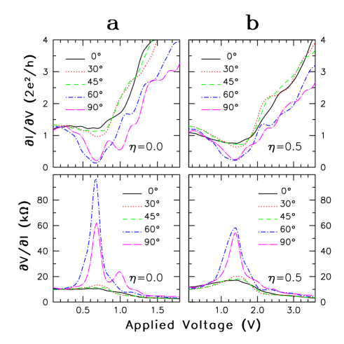
Once the transmission function is computed, the determination of the differential conductance and resistance is straigtforward. Figure 4 shows the results for two extreme cases of equilibration of the Fermi levels. The first is when (Figure 4a), and the symmetric case (Figure 4b). When =0.0, the Fermi level of the NT follows exactly the applied voltage on one gold pad and the conductance spectrum is directly proportional to . As expected, there is no large difference between the 0∘, 30∘ and 45∘ models, while the 60 and 90∘ models show the dip structure at around 0.6 V. The non-linear resistance (NLR) spectra show clearly a sharp increase by almost an order of magnitude at 0.6 V. These features are also observed when =0.5, where the Fermi level of the NT is floating at half the voltage applied between the two gold pads. The dip at around 1.2 V in the conductance spectra is now broader, and the NLR of the 60∘ bent tube increases by about a factor of 4 from the computed resistance of the straight tube. These results suggest that there exists a critical bending angle (between 45∘ and 60∘) above which the conduction in armchair carbon nanotubes is drastically altered [28].
In conclusion, we have calculated the effects of structural distortions of armchair carbon nanotubes on their electrical transport properties. We found that bending of the nanotubes decreases their transmission function and leads to an increased electrical resistance. The effect is particularly strong at bending angles higher than 45∘ degrees when the strain is strong enough to lead to kinks in the nanotube structure. The electronic structure calculations show that the reduction in is correlated with the presence at the same energy of localized states with significant - hybridization due to the increased curvature produced by bending. Resistance peaks near are the likely cause for the experimentally observed low temperature localization in carbon NTs bent over metal electrodes [7]. Our calculations of the resistance (including the contact resistance) of a perfect NT give a value close to instead of . This increase in resistance is solely due to the finite transmission of the contacts. The much larger contact resistances observed in many experiments on SWNTs are likely due to the weaker coupling of the NT to the metal when the NT is simply placed on top of the metal electrodes. We predict that NTs end-bonded to metal pads will have contact resistances of only a few k. Such low contact resistances will greatly improve the performance of NT-based devices and unmask the Q1D transport properties of NTs.
REFERENCES
- [1] M.S. Dresselhaus, G. Dresselhaus, and P.C. Eklund, Science of Fullerenes and Carbon Nanotubes (Academic, San Diego, 1996).
- [2] S.J. Tans, A.R.M. Verschueren, and C. Dekker, Nature 393, 49 (1998).
- [3] M. Bockrath, D.H. Cobden, P.L. McEuen, N.G. Chopra, A. Zettl, A. Thess, and R. E. Smalley Science 275, 1922 (1997).
- [4] P.G. Collins, A. Zettl, H. Bando, A. Thess, and R.E. Smalley, Science 278, 100 (1997).
- [5] R. Martel, T. Schmidt, H.R. Shea, T. Hertel, and Ph. Avouris, Appl. Phys. Lett. 73, 2447 (1998).
- [6] C.T. White, and T.N. Todorov, Nature 393, 240 (1998).
- [7] A. Bezryadin, A.R.M. Verschueren, S.J. Tans, and C. Dekker, Phys. Rev. Lett. 80, 4036 (1998).
- [8] L. Chico, L.X. Benedict, S.G. Louie, and M.L. Cohen, Phys. Rev. B 54, 2600 (1996).
- [9] M.P. Anantram, and T.R. Govidan, Phys. Rev. B 58, 4882 (1998).
- [10] T. Hertel, R. Martel, and Ph. Avouris, J. Phys. Chem. B 102, 910 (1998).
- [11] T. Hertel, R.E. Walkup, and Ph. Avouris, Phys. Rev. B 58, 13870 (1998).
- [12] S. Iijima, C. Brabec, A. Maiti, and J. Bernholc, J. Chem. Phys. 104 2089 (1996).
- [13] M.R. Falvo, G.J. Clary, R.M. Taylor II, V. Chi, F.P. Brooks Jr, S. Washburn, and R. Superfine Nature 389, 582 (1997).
- [14] C.L. Kane, and E.J. Mele, Phys. Rev. Lett. 78, 1932 (1997).
- [15] A. Rochefort, D.R. Salahub, and Ph. Avouris, Chem. Phys. Lett. 297, 45 (1998).
- [16] A. Rochefort, D.R. Salahub, and Ph. Avouris, J. Phys. Chem. 103, 641 (1999).
- [17] Landrum, G. YAeHMOP (Yet Another Extended Hückel Molecular Orbital Package), Cornell University, Ithaca, NY, 1995.
- [18] S. Datta, Electronic Transport in Mesoscopic Systems, (Cambridge University Press, Cambridge, U.K., 1995).
- [19] W. Tian, S. Datta, S. Hong, R. Reifenberger, J.I. Henderson, and C.P. Kubiak, J. Chem. Phys. 109, 2874 (1998).
- [20] N.D. Lang, and Ph. Avouris, Phys. Rev. Lett. 81, 3515 (1998).
- [21] E.N. Economou, Green’s Functions in Quantum Physics, (Springer-Verlag, New York, 1983).
- [22] D.A. Papaconstantopoulos, Handbook of the Band Structure of Elemental Solids, (Plenum Press, NY 1986).
- [23] N.L. Allinger, Y.H. Yuh, and J.-H. Lii, J. Am. Chem. Soc. 111, 8551 (1989).
- [24] Y. Kong, and J.W. Ponder, J. Chem. Phys. 107, 481 (1997).
- [25] The coupling strength depends on the amount of charge transfer, i.e. the difference in the work functions of the NT and the metal, and the area of the contact.
- [26] P. Kim, T. W. Odom, J. L. Huang, and C. B. Lieber, Phys. Rev. Lett. 82, 1225 (1999).
- [27] A. Bachtold, M. Henny, C. Terrier, C. Strunk, C. Schönenberger, J.-P. Salvetat, J.-M. Bonard, and L. Forró , Appl. Phys. Lett. 73, 274 (1998).
- [28] The assumption that the potential drops linearly across the NT is particularly drastic for highly bent models. In reality, in the highly deformed region, the voltage would drop in the vicinity of defects. This voltage drop near defects would decrease the transmission probability of the propagating electrons, and consequently emphasize the magnitude of the changes we have computed with our first assumption.