Single Spin Measurement using Single Electron Transistors
to Probe Two Electron Systems
B. E. Kane*, N. S. McAlpine, A. S. Dzurak, R. G. Clark
Semiconductor Nanofabrication Facility
School of Physics, University of New South Wales
Sydney 2052 AUSTRALIA
G. J. Milburn, He Bi Sun, and Howard Wiseman
School of Physics, University of Queensland
St. Lucia 4072 AUSTRALIA
()
Abstract
We present a method for measuring single spins embedded in a solid by probing two electron systems with a single electron transistor (SET). Restrictions imposed by the Pauli Principle on allowed two electron states mean that the spin state of such systems has a profound impact on the orbital states (positions) of the electrons, a parameter which SET’s are extremely well suited to measure. We focus on a particular system capable of being fabricated with current technology: a Te double donor in Si adjacent to a Si/ interface and lying directly beneath the SET island electrode, and we outline a measurement strategy capable of resolving single electron and nuclear spins in this system. We discuss the limitations of the measurement imposed by spin scattering arising from fluctuations emanating from the SET and from lattice phonons. We conclude that measurement of single spins, a necessary requirement for several proposed quantum computer architectures, is feasible in Si using this strategy.
PACS number(s): 85.30.Wx, 76.20.+q, 03.67.Lx
*Current address: Laboratory for Physical Sciences, University of Maryland, College Park MD 20740. e-mail: kane@lps.umd.edu
1 Introduction
The detection of a single electron or nuclear spin is perhaps the ultimate goal in the development and refinement of sensitive measurement techniques in solid state nanostructure devices. While of interest in their own right, single spin measurements are particularly important in the context of recently proposed solid state quantum computers, where electron [1] [2] [3] and nuclear [4] spins are qubits which must be initialized and measured in order to perform computation. Methods proposed for measuring single electron spins include using a sensitive magnetic resonance atomic force microscope [5] [6] and detecting charge transfer across magnetic tunnel barriers [7]. Sensitive optical techniques may also be promising [8]. Even if these techniques cannot readily be integrated into a quantum computer architecture, single spin measurements will be invaluable for measuring the electromagnetic environment of the spin, which will determine the decoherence mechanisms ultimately limiting a quantum computer’s capability.
Here we discuss a method for probing the spin quantum numbers of a two electron system using a single electron transistor (SET). Because of the Pauli Exclusion Principle, spin quantum numbers of such systems profoundly affect the orbital states (positions of the two electrons) of the system. Recently developed SET devices are extraordinarily sensitive to charge configuration in the vicinity of the SET island electrode, and they can consequently be used to measure the spin state of two electron systems in appropriate circumstances. In the scheme previously proposed [4], electron transfer into and out of bound states on donors in Si are measured to determine whether the electrons are in a relative singlet or triplet configuration. SET’s have already been proposed for performing quantum measurement on qubits in a Josephson Junction-based quantum computer [9]. SET’s, operating at temperature 100 mK, have the recently demonstrated capacity to measure charge to better than at frequencies over 200 MHz [10].
Several material parameters make Si a good choice in which to fabricate single spin measuring devices: spin orbit coupling is small in Si, so the phonon- induced spin lattice relaxation rate is almost seven orders of magnitude smaller in Si [11] than it is in GaAs [12]. Also, nuclear isotopes with nonzero spin can in principle be eliminated in Si by isotope purification. The bound states on Si donors have been thoroughly characterized and studied. A complication of Si arises from its sixfold degenerate band structure. We will focus on Si devices in this paper, but the ideas presented here can be readily generalized to other material systems.
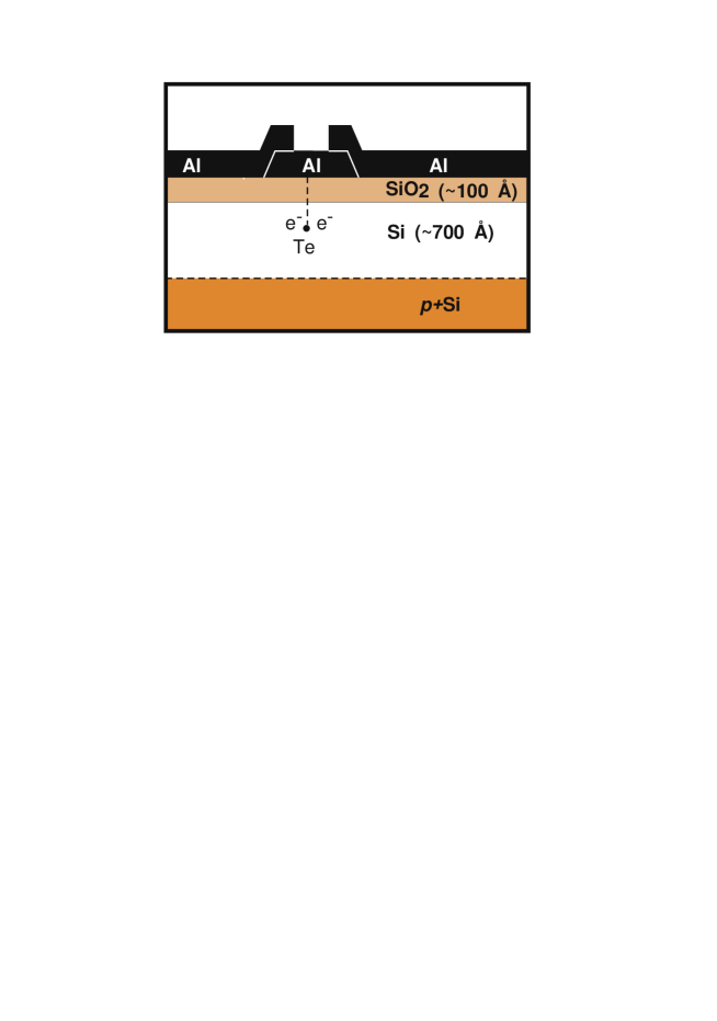
The configuration we will study is extremely simple (Fig. 1): a SET lies directly above two electrons bound to a single donor impurity in an otherwise undoped layer of a Si crystal. Such a two-electron system, which can be thought of as a solid state analog of a He atom, can be created in Si by doping with S, Se, Te, or Mg [13][14]. A barrier layer isolates the SET from the Si, and the substrate is heavily doped, and hence conducting, beginning a few hundred Å below the donor. As drawn in Fig. 1 the device requires careful alignment of the SET to the donor; however, the ideas in this paper could be verified using a scanned probe SET [15], and the Te donor could be deposited by ion implantation, so no nanofabrication on the Si would be required.
The ground state of the electrons on the donor is a spin singlet. The experiment proceeds by applying a voltage between the SET and the substrate just sufficient to ionize the donor and draw one electron towards the interface. In this situation small changes in the applied voltage cause the electron to move between the donor and the interface, and this electron motion will change the SET conductance. If the electrons are in a spin triplet state, however, no bound state of appropriate energy exists on the donor, and no charge motion will be observed. All the donors listed above have stable isotopes with both zero and nonzero nuclear spin. If the donor is a nucleus with nonzero spin, strong hyperfine interactions couple the nuclear spin to the electrons, and the nuclear spin can be inferred from measurements of the motion of the electrons. The measurement of both electron and nuclear spin will require that the electron Zeeman energy exceed so that the electron spin states are well resolved, a condition which is readily met in Si at a temperature T100 mK and magnetic field 1 T.
2 Experimental Configuration
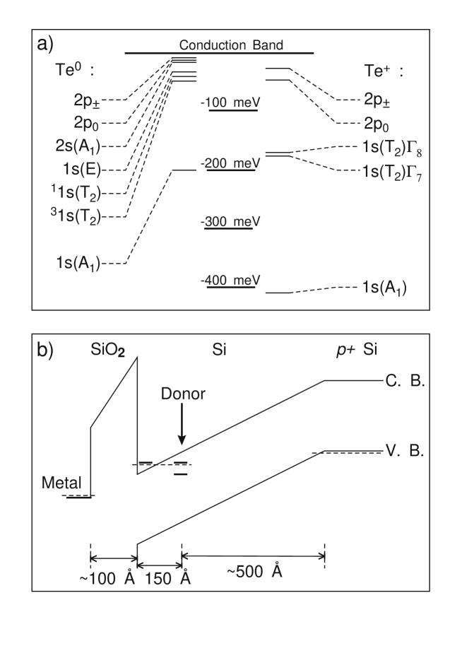
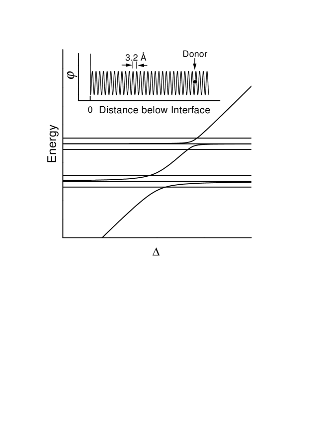
Of the several possible two-electron donors in Si, we will focus on Te for two reasons: firstly, its energy levels are the shallowest of the Group VI donors [13], enabling it to be ionized by a relatively modest applied electric field. Secondly, it is a reasonably slow diffuser in Si [16], and thus should be compatible with most Si processing techniques. The bound state energies of Te donor states are shown in Fig. 2a. and ground states are respectively 200 and 400 meV below the conduction band.
Electron orbital states in the Si conduction band have a six-fold valley degeneracy, with valley minima located along the [100] directions 85% of the distance to the Brillouin zone boundary. This degeneracy is broken in states at a donor by the central cell potential into a singly degenerate state, a triply degenerate state, and a doubly degenerate E state. The state, which is a linear combination of each of the six valleys, is the only state which has a finite probability density at the donor site, and consequently has the lowest energy, owing to the central cell attractive potential. In two electrons lie in the state in a nondegenerate spin-singlet configuration. This state is over 150 meV below the excited states, including the lowest lying triplet configuration of the two electron spins [14] [17].
In the proposed measurement configuration, an electric field is applied so that an electron on the Te donor is weakly coupled to a state at a [100] oriented Si/ interface (Fig. 2b). The condition that the donor and interface states be weakly coupled requires that the distance between the donor and the interface must be 100-200 Å. Pulling the electron to the interface will thus require =1-2 mV/Å=0.1-0.2 MV/cm. in the layer will be approximately three times bigger owing to the smaller dielectric constant in . (; .) At these fields Fowler-Nordheim tunneling across a 100 Å barrier or between the Si valence and conduction band is negligible [18], so charge will not leak into or out of the donor or interface states. The substrate must be doped, however, so that the carriers in the substrate will be repelled from the interface by .
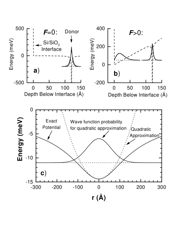
When =0, both electrons are bound to the Te donor (Fig. 3a); however, one electron will occupy an interface state when is sufficiently large (Fig. 3b). In Si, the electron mass in each valley is anisotropic with and [19], masses corresponding to motion parallel and perpendicular to the valley axis respectively. At a [100] oriented Si/ interface, the sixfold valley degeneracy of electron states is broken, and lowest energy states correspond to the two valleys along the axis perpendicular to the interface.
When it is not located at the Te donor, the electron is still attracted to the donor by its net positive charge. While this attraction is counteracted by in the direction, perpendicular to the interface, the electron is drawn toward the donor in the plane, resulting in the potential drawn in Fig. 3c. Thus, the electron at the interface is still weakly bound to the donor.
The energies of the electron interface states will be the sum of the binding energies in the and in the directions. We assume that the confinement can be approximated by a triangular potential. The energies of the states are [19]:
| (1) |
for 1. For and =2 mV/Å, =59 meV and =104 meV. The ground state electron probability density function is peaked at a distance 20 Å from the interface and falls off rapidly at large distances. The effect of the donor a distance =100-200 Å from the interface is minimal on the interface energy levels, but weak tunneling between the donor and the interface is still possible. For modeling of the system, we will assume =125 Å.
The potential in the plane is:
| (2) |
Here, is the distance in the plane from the point in the plane nearest the donor. Because the electron sees an attractive image charge associated with the Si/ dielectric boundary, . This potential is easily approximated by a parabolic potential, leading to the following energies:
| (3) |
for . For , =6 meV and =9 meV. The probability density for the parabolic approximation wave function, plotted in Fig. 3c, is only large in the region where the potential is well approximated by a parabola, indicating that the parabolic approximation is justified. An applied will modify these energies significantly if the cyclotron energy, , becomes comparable to the state energy differences [20]. However, at =1 T in Si, 0.6 meV, so magnetic modification of the orbital states should be minimal.
These results show that the lowest lying interface state is about 65 meV above the conduction band, separated from the first excited state by 3meV. These states are in the valleys along the -axis. Energies of the states in the valleys along the and axes are 40 meV higher in energy. Because there are two valleys along the axis, the electron interface states are still two-fold degenerate. Sham and Nakayama [21] have shown that this degeneracy is lifted by the sharp Si/ interface potential in the presence of an applied electric field. They estimate 0.5 Å, corresponding to a splitting of 1 meV for the proposed measurement configuration. Although small, this splitting is sufficient to insure that the interface electron occupies a single valley state at 1K.
3 Simplified Model Hamiltonian
We model the system using a simple Hamiltonian for the two electrons: they can be in only two spatial states: either located at the donor or at the interface . Additionally, the two electrons can be in one of two spin states or . Of the sixteen possible configuration states of two electrons in the model, only six are antisymmetric with respect to particle interchange, and are appropriate for electrons.
Measurements will be made in the regime where the energy of the state in which both electrons lie on the donor, , is nearly degenerate with the states in which one electron is at the donor and one is at the interface, and . The removal of both electrons from the donor requires an additional 400 meV of energy (the binding energy of the ground state). Consequently, we neglect the state in which both electrons are at the interface, since it is of much higher energy than the others. The five remaining antisymmetric basis states, eigenstates of both the particle and spin exchange operator, are:
| (4) |
where we have neglected normalization factors. In the simplest approximation, there are three terms in the Hamiltonian: , the energy difference between the and the states, can be varied by the bias applied between the substrate and the SET island electrode. The energy difference between and states is the Zeeman energy, where is the Bohr magneton and is the Landé factor. is the amplitude for the electron to tunnel from the donor state to the interface state. The Hamiltonian matrix of the system is:
| (5) |
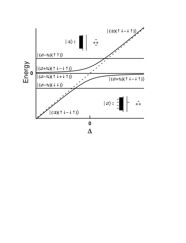
The energy levels of this system, plotted as a function of , are shown in Fig. 4. Because of the overall antisymmetry of the electron wave function, the state must be a spin singlet: . A spin singlet state is also possible with a symmetric spatial state of one electron on the donor and one at the interface . Hybridization of these two levels results in the anticrossing behavior seen in Fig. 4. In this system the only possible spin triplet levels are associated with the spatially antisymmetric state . The energy of these three states, although split by the magnetic field, are unaffected by the applied electric field. Consequently, the spin singlet states are polarizable by an applied electric field, while the spin triplet states are not. This fact illustrates how an electrical measurement can in principle determine a spin quantum number.
4 Measurement Procedure
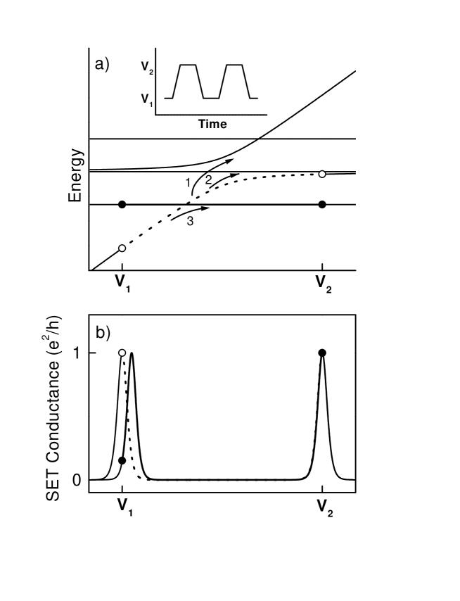
The difference in electric polarizability of singlet and triplet spin states discussed above can be detected by a SET. SET’s are typically fabricated from Al, with a small island electrode weakly coupled to two leads (the source and drain) through thin tunnel barrier layers (Fig. 1). For sufficiently small islands and at low temperatures the Coulomb blockade prevents electron transport across the island unless a discrete energy level of the island is resonant with the Fermi level in the source and drain. A SET can function as a sensitive electrometer because this resonance condition is sensitive to any potentials coupling to the island - for example, coming from the substrate in Fig. 1. The SET shown will exhibit periodic conductance peaks with magnitude of order as a function of substrate bias, each corresponding to the addition of one electron to the island. Charge motion in the vicinity of the SET changes the island potential and results in shifts in the substrate bias voltage at which the peaks occur.
Figure 5 depicts both the energy levels of the two electron system as a function of and the conductance of the SET as a function of substrate bias. For simplicity we assume that the SET conductance peaks are spaced symmetrically away from the point where the electron levels cross ( = 0). (The conductance peaks can be moved to any position relative to the level crossing by applying a voltage to an additional remote electrode, weakly coupled capacitively to the SET.) The measurement proceeds by measuring the SET conductance on both sides of the level crossing (at voltages and ) by applying a voltage waveform to the substrate similar to that shown in the inset to Fig. 5a. The measurement must distinguish whether the electrons are in the lowest energy spin singlet or the lowest energy spin triplet state. At one electron is on the donor and one electron is at the interface for both singlet and triplet states, so the SET island potential - and hence the SET conductance - is the same for both triplet and singlet states. At , however, the singlet state is in a configuration where both electrons are on the donor, while in the triplet state the electron positions are the same as they were at . This difference in the electron positions results in a difference in the potential at the island, and hence a difference in the voltage at which the SET conductance maximum occurs. This conductance change can thus be used to infer the spin state of the two electrons.
The size of the offset between triplet and singlet conductance peak positions is determined by how well the electrons are coupled to the SET island and how far the electron moves. If the electron moved all the way from the conducting substrate to the island, the conductance peaks would be offset by one electron. The approximate peak position change for smaller electron movement is given by the ratio :
| (6) |
where and are the thicknesses of the and undoped Si layers, respectively, and is the distance which the electron moves. For the layer thicknesses shown in Fig. 1 and = 125 Å, =0.12. Thus, the conductance peaks of the SET can be offset approximately 10% by the motion of the electrons between the donor and interface states.
A charge sensitivity of 0.1 is readily achievable with SET’s and has been demonstrated with the recently developed RF-SET’s [10], which are capable of fast (100 MHz) measurements. These RF-SET’s have a demonstrated charge noise of , implying that the SET can measure 0.1 in 0.25 sec. High speed operation of the SET’s may be necessary for the measurement because the measurement must occur on a time short compared to the time the electron scatters between spin states. Spin scattering and fluctuations are not included in the simplified Hamiltonian of Eq. 5 but will be present in real systems, and will be discussed below.
In principle, a single conductance measurement at would be sufficient to determine the spin state of the electrons, and the need to measure repeatedly at and at would be unnecessary. However, motion of remote charges will also couple to the SET [22] leading to drifting of the conductance peak positions (1/ noise). AC modulation of the substrate bias can be used to measure the separation between adjacent conductance peaks, rather than their absolute position, and so can eliminate this drift from the measurement.
5 Effect of Fluctuations
If the terms in Eq. 5 fluctuate, the energy levels shown in Fig. 4 will not necessarily be eigenstates of the system, and transitions between states will be possible. Fluctuations will arise due to lattice vibrations, and also will inevitably emanate from the SET, since tunneling of electrons on and off of the SET island is a random process. A rigorous approach to the effect of SET fluctuations must treat the SET and the electrons being probed as a coupled quantum system. Master equation techniques can be applied to this problem, and have been used to analyze the system of a Josephson Junction qubit coupled to a SET [9] and tunneling devices [23]. While a similar analysis of a two electron system coupled to a SET is in preparation [24], we will proceed by assuming that scattering of the electrons is driven by external classical fluctuating fields, the magnitudes of which we estimate from experimental conditions. The scattering times so derived will then be compared to the measurement time, derived above.
Fluctuations in the occupancy of the SET island will couple into the electron system via , the potential difference between the donor and interface states. Phonon-induced fluctuations are, however, the dominant mechanism of electron spin relaxation in lightly doped Si, measured in electron spin resonance (ESR) experiments [25]. The degeneracy of the six conduction band valleys is broken by uniaxial stress directed along the [100] directions, with compression lowering the energy of the two valleys along the strain axis with respect to the other four valleys. To first order strain does not affect the energy of the donor ground state, which is composed of equal amounts of each of the six valleys, but the interface state energy level will shift with respect to the donor state level with the application of strain. Thus, phonons will also lead to fluctuations in . Additionally, both bias and phonon fluctuations couple to the term in the Hamiltonian, a mechanism of relaxation which we will consider separately below.
6 Scattering between Spin Singlet States
We treat the simplest case first, the effect of fluctuations in on the two spin singlet states of Eq. 5:
| (7) |
The Hamiltonian is exactly diagonalized by rotating the basis states though an angle . For fluctuations in , the relaxation rate between the eigenstates of Eq. 7 is given by:
| (8) |
where and is the spectral density of fluctuations of evaluated at the transition frequency between eigenstates. The magnitude of determines the degree to which the fluctuations couple between the eigenstates, and scattering is reduced when . Larger values of , far away from the anticrossing region, will lead to smaller scattering rates between the coupled singlet states if is constant.
To determine an explicit value for , we need to know . For voltage noise emanating from the SET, can be determined from the time dependence of the charge on the SET island electrode. The high frequency dynamics of SET’s is still a topic of research, and will depend sensitively on capacitances and inductances of the SET and in the external circuit. To obtain crude estimates of relaxation times, we will simply assume that SET noise is frequency independent shot noise determined entirely by the SET current and the SET resistance:
| (9) |
where , , and are the voltage, current and small signal resistance of the SET. This leads to:
| (10) |
where , defined in Eq. 6, determines the proportion of voltage that drops between the donor and interface states.
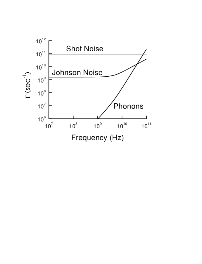
A quiescent SET, in which =0, will generate a much smaller amount of noise, especially if the island is biased so that . Again, for the purpose of generating crude estimates, we assume that quiescent SET noise is given by Johnson noise () when the SET is at a conductance peak. To determine the magnitudes of shot noise and Johnson noise, we use parameters tabulated by Schoelkopf for an optimized RF-SET [10] biased to maximum sensitivity ( 1 mV, = 50 k, =100 mK) in a configuration in which =0.1. Using these numbers maximal scattering rates (using Eq. 8 with =1) are plotted in Fig. 6. Realistic values of the capacitance of the SET, which has been entirely neglected in the foregoing, will tend to roll off the spectra at frequencies 10 GHz. Thus, the data constitutes an upper bound on the scattering rates to be expected.
The magnitude of fluctuations in induced by phonons is determined by , the deformation potential, which is the rate the valley energy varies as strain is applied, and by the density of states of phonons at a given frequency. A straightforward calculation leads to:
| (11) |
where is the density of the Si crystal and and are the velocities of longitudinal and transverse acoustic phonons respectively. Angular dependences of the phonon couplings have been neglected in Eq. 11, as has the presence of the nearby surface, which will modify the phonon spectrum at low frequencies. Thus, Eq. 11 only provides an approximate relaxation rate, which is plotted in Fig. 6 for =100 mK and =1. This expression includes vacuum fluctuations, and is thus only appropriate for transitions from higher to lower energy states when . While the phonon contribution to rises rapidly as a function of frequency, it only exceeds the shot noise contribution at frequencies approaching 100 GHz.
To obtain approximate transition rates between the singlet states using the shot noise expression, we assume =100 GHz and = 1 GHz, so . With these values, we obtain or a decay time of 0.1 sec. This time is almost the same as the time estimated above for RF-SET’s to measure the spin state of the two electron system. It is likely that our use of a frequency independent shot noise is an overestimate, and that the relaxation time exceeds the measurement time. Also, the measurement time can possibly be reduced a factor of 10-100 in optimized SET devices [10].
7 Scattering between Different Spin States
At first glance, it would appear that the measurement time be less than the singlet-singlet scattering time in order for spin detection to be viable. However, the point of the measurement procedure is to distinguish between the lowest lying singlet and triplet states. Scattering between these states (labeled “3” in Fig. 5) must not occur. However, scattering between the other states can occur so long as the average electron position difference between the singlet and triplet states is resolvable. Type 3 scattering must occur through spin flips and in general will be much weaker than scattering between the electric dipole coupled singlet states. This is a crucial distinction between the measurement of spin using SET’s and the measurement of charge quantum states, such as those in Josephson Junction qubits [9], where the states are electric dipole coupled.
The Hamiltonian of Eq. 5 is obviously oversimplified, since no terms couple different spin states, and no spin relaxation is possible. The dependence of the electron factor on external conditions, and in particular on band structure parameters, is the major source of spin relaxation in Si [25] and consequently must be included in a more accurate model of a two electron system in Si. The extremely long relaxation times measured in Si at low temperatures (1000 sec.) [11] are a consequence of the fact these parameters are small in Si. Additionally, if the electrons can exchange spin with other particles, in particular with nuclear spins, then scattering between different electron spin states will occur.
The factor of an electron in a conduction band valley in Si is not exactly equal to the free electron value and is slightly anisotropic, a consequences of spin orbit coupling. The anisotropy leads to a modified one electron spin Hamiltonian:
| (12) |
where are the Pauli spin matrices, and is the angle of with respect to the valley () axis. If the axis is redefined to be along , the spin Hamiltonian becomes:
| (13) |
where:
| (14) |
and:
| (15) |
The anisotropy will be the same for each of the two valleys comprising the interface states; however, since the donor state is an equal admixture of all six valleys, its -factor will be isotropic=. For two electron systems, the spin dependent corrections to the Hamiltonian in Eq. 5 are:
| (16) |
At the conduction band in Si, =1.99875 [26]. , measured by applying strain to shallow donors [25], is 1.0. Finally, for =2.0023 [27]. The off-diagonal terms, which will lead to scattering between spin states if fluctuations are present, are each and are small perturbations on the original Hamiltonian. The term will vanish, in principle, if is precisely aligned along a [100] axis of the crystal, perpendicular to the interface, and this orientation will presumably be the optimal experimental configuration.
To obtain an estimate for scattering rates between spin states, an approximate solution to the full Hamiltonian (Eqs. 5 and 16) must be calculated. The solution is complicated by the fact that the and states (the states with energy in Fig. 4) are nearly degenerate when 1, a degeneracy also weakly broken by the difference in factors at the donor and interface states. To obtain an approximate solution, valid in the measurement regime when 1, we first diagonalize the Hamiltonian matrix to second order in , which lowers the state energy with respect to by . The and submatrix is then diagonalized exactly by rotating the basis states through an angle , where:
| (17) |
Finally, corrections to the resultant wave functions are determined to first order in the remaining terms of Eq. 16.
Once the perturbed wave functions are known, the matrix elements coupling states generated by fluctuating terms may be easily determined. For a fluctuation of the form the perturbation Hamiltonian matrix is given by:
| (18) |
Only lowest order terms have been retained, and we have simplified the expression by writing . These matrix elements may be inserted directly into Eq. 8 to determine scattering rates between states induced by fluctuations in .
The matrix elements for scattering into and out of (state ) contain a term in addition to the present in the terms scattering between the singlet states discussed above. Neglecting entirely the angular dependence of and using , , resulting in a total scattering rate out of the state of about 0.3 for the same conditions used to calculate the scattering rate between the singlet states above. This result suggests that very long averaging times of the SET measurement will be possible before spin relaxation occurs, and that single spin measurement in Si will be possible in appropriately designed devices.
In experimental conditions will be sufficient to effectively polarize the electrons, i.e. . At =100 mK, this requires that 0.7 T and 10 GHz. For =1 GHz and =100 GHz, this implies that 1 and that scattering to states and (labeled respectively ’1’ and ’2’ in Fig. 5) will be comparable. As mentioned above, this type of scattering will not harm the measurement as long as the average positions of electrons in the states being distinguished differs.
8 Scattering Induced by Fluctuations of
The calculation leading to Eq. 18 may be repeated to determine the effect of fluctuations in on scattering between states. The result is:
| (19) |
Because of the absence of the term present in most of the matrix elements of Eq. 18, fluctuations in will have a greater effect on scattering than fluctuations in if the fluctuations are of the same magnitude.
Band structure effects in Si can further magnify the importance of fluctuations. In Si the valley minima are located at , where =5.43 Å is the lattice constant. If valleys on opposite sides of the Brillouin zone are coupled to each other at two points in real space (at two donors or at a donor and an interface), standing waves with node spacing appear in the coupling between the two sites. These rapid oscillations have been previously analyzed in the context of the exchange interaction between donors in doped Si [28]. For a donor located near an interface which breaks the valley degeneracy, the coupling between the donor states and the two valley states at the interface is a rapidly oscillating function of the separation between the donor and the interface (Fig 7). If is a rapidly oscillating function of external parameters, fluctuations in the external parameters will be strongly amplified.
The magnitude of this effect may be most readily estimated when the fluctuations arise from strain. As mentioned above, strain shifts the energies of the valleys along the strain axis relative to the valleys on axes perpendicular to the strain axis. Strain, , will also change the value of , the location of the valley minima, and hence the wavelength of the standing waves. We are unaware of measurements of but estimate its order of magnitude by assuming that the effect of strain on electron energy levels is linear in in the neighborhood of the valley minimum on the axis:
| (20) |
where is the direction along the valley axis. We entirely neglect effect of the orientation of the applied strain. Here, is the deformation potential introduced above = 9 eV in Si. From this equation, we obtain:
| (21) |
Assuming , we obtain the maximum effect of the strain as:
| (22) |
For =1 GHz, and =125 Å, the term in brackets is . This is the magnitude of phonon-induced fluctuations relative to fluctuations. For , the conditions considered above, scattering rates attributable to fluctuations in will be four orders of magnitude larger than those from fluctuations. While the derivation leading to this result is highly approximate, it does suggest that fluctuations may be neglected, despite the amplifying effect of oscillations induced by band structure.
Fluctuations in the voltage bias, or in the electric field in the vicinity of the electrons, will also lead to fluctuations in . It would seem that the effect of an electric field, highly uniform on the scale of the lattice, would be small on intervalley coupling. However, the applied bias does change the area on the interface where the electron wave function is sizable, and the valley splitting induced by the interface will be highly sensitive to the morphology of the interface, and hence is very difficult to estimate. While we do not have a numerical estimate for bias-induced fluctuations, it seems unlikely that they will be an important source of scattering between states.
9 Additional Sources of Noise in the Electromagnetic Environment
The major source of both electric dipole and spin flip scattering in the electromagnetic environment arises from the fluctuating electric field generated by the SET. Because the SET is a high impedance device, with resistance of order , the ratio of the magnetic to the electric field generated by the SET is =1/137 in cgs units. , the ratio of magnetic to electric interaction energies of the SET with the electrons is . This leads to a spin relaxation rate induced by the field emanating from the SET of , which can be neglected.
A more relevant source of fluctuations arises because RF-SET’s are AC devices, biased by a tuned circuit oscillating at GHz. GHz frequencies are employed to minimize the contribution of noise from GaAs field effect transistors (FET’s) amplifying the SET output. Because the tuned circuit must be near the SET, the device will be exposed to both electric and magnetic fields at the SET bias frequency. Consequently, the electron energy state differences will need to be away from the SET bias frequency and its harmonics during measurement. Doing measurements at magnetic fields when =10-20 GHz should fulfill this requirement.
10 Scattering between States at Level Crossings
To perform repeated measurements on the system, it will be necessary to traverse the region where the two spin levels cross one another (Figs. 4 and 5). If there is a small coupling between the two states, an anticrossing will occur, and scattering will occur between the levels if the crossing region is not traversed sufficiently rapidly. Ideally however, the passage should be “adiabatic” with regard to the strongly coupled singlet states, so that these states simply follow the levels plotted in Figs. 4 and 5 as is varied. These two requirements imply that there is an optimal value for the traversal rate, , where undesired scattering is minimized. As mentioned above, however, scattering between the states being distinguished is much more harmful than scattering between the singlet states, implying that be as large as possible. Additionally, even though the SET can be turned off during traversal, some noise in the environment will be present during the passage (the Johnson noise and the phonons, plotted in Fig. 6), and a rapid traversal rate will minimize the contribution of this noise to scattering at the level crossing.
A simple Golden Rule calculation determines the scattering probability between two crossing levels as a function of . The result is:
| (23) |
where is the energy difference between the levels at the anticrossing point. A likely upper limit to the traversal rate is of order 100 GHz/nsec =. We first estimate the scattering resulting from the term in Eq. 16, again neglecting its angular dependence: =10 MHz. These values result in .
Spin scattering can also occur near the crossing point through the exchange of electron spin with nuclear spins in the lattice, since natural Si contains 5% 29Si with =1/2. The small value of the nuclear Zeeman energy compared to the electron Zeeman energy means that such scattering can only occur near the level crossing point. The electron interaction with 29Si will be dominated by the contact hyperfine interaction [29]:
| (24) |
where is the electron probability density at the nuclear site. Evaluation of for the hyperfine interaction entails an appropriate average over all lattice sites, assuming that the total polarization of the nuclei is zero:
| (25) |
The numerator in this expression is exactly the same average as that used to determine the mean square line width of donor ESR lines, a parameter which has been measured for Si:Te [27]. In using Si of natural isotopic composition, the ESR line width is 30 MHz, leading to an estimate of . Interaction with lattice nuclei could be further reduced if necessary by using Si depleted of 29Si. These results imply that perhaps thousands of passes across the level crossing can be made before a spin scattering event occurs.
11 Extension to Nuclear Spin Measurement
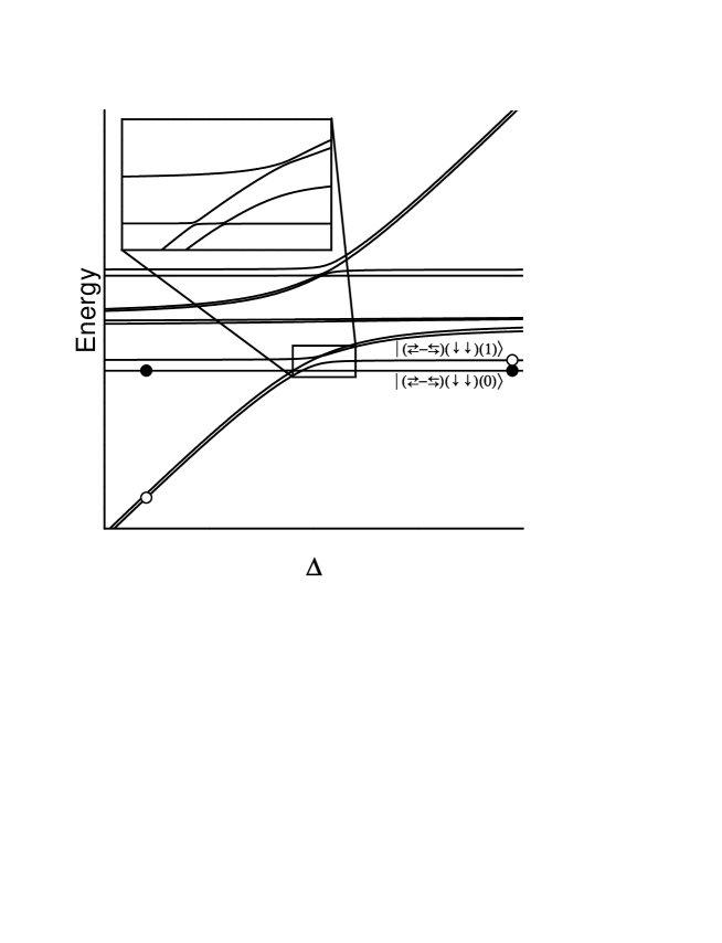
In the foregoing discussion we have implicitly assumed that the nuclear spin on the Te donor is zero. While Te is composed of 92% stable isotopes, 7% of natural Te is , with =1/2. For the donor level, the electron spends approximately 10% of its time on the donor site, and consequently in Eq. 24 can be large [27] [30]. For Si: the zero level splitting induced by hyperfine interactions is 3.6 GHz, which is comparable to the electron Zeeman splitting for =0.1 T.
The levels for a coupled two electron- and one nuclear-spin system are plotted in Fig. 8, with the small nuclear Zeeman energy splitting greatly exaggerated so that the levels may be distinguished. The electron Hamiltonian is that of Eq. 5, while the nucleus couples only to electrons at the donor site by the contact hyperfine interaction. The Hamiltonian again does not contain any terms that change the total component of angular momentum of the system, and the state with all spins pointing in the same direction (designated in Fig. 8) does not hybridize with other states. The nuclear spin state in which the nuclear spin points opposite to the electrons does hybridize with the electron spin singlets that couple to the applied bias , leading to the separation of the nuclear spin states shown in Fig. 8.
Measurement of the nuclear spin state proceeds in a manner entirely analogous to the spin measurement of the electron discussed above. SET conductance peak positions are measured at two fixed points on opposite sides of the level crossing. As in the case with electrons, scattering between the electric dipole coupled states can occur during the measurement, so long as scattering does not take place between the states being distinguished. As in the case with electrons, these latter types of scattering processes will occur as a result of electron fluctuations, impurity nuclear spins, and nuclear and electron dipole interactions. Since the magnitudes of these effects are similar for the electron and nuclear spin measurement problem, it does not appear that measurement of nuclear spins will be intrinsically more difficult than of electron spins.
12 Experimental and Materials Issues
We have focused on the Si/ material system for single spin measurement devices, primarily because of the wealth of data in Si on ESR of donors. These ideas may be viable in other systems, and possibly in GaAs/AlxGa1-xAs heterostructures, if the greater spin-orbit and hyperfine interactions in these materials do not pose insurmountable problems. The lesser quality of the Si/ interface compared to GaAs/AlxGa1-xAs should not affect the proposed devices: a mobility of implies energy fluctuations on the Si/ interface of order 0.5 meV, less than the lateral binding energy of the interface electrons to the donor calculated above. We have neglected entirely the effects of the layer on the resonance and relaxation of the electrons. ESR of conduction electrons at the Si/ interface is very difficult to measure [31] [32], so experimental data on the effect of the interface is lacking.
Initial experiments will most simply be carried out on samples randomly doped with Te by ion implantation or diffusion, and the measurements made with a scanned SET so that many donors can be tested for possible single spin sensitivity. Even if a scanned probe SET is used, the material will have to be extraordinarily free () of bulk and interface spin and charge impurities in order to have a reasonable probability of success in measuring a single spin, a requirement that may prove very difficult to meet using conventional Si processing. SiGe heterostructures may be an attractive alternative system [3] if problems associated with interface states and dangling bonds in Si/ structures prove to be insurmountable.
Finally, in order to demonstrate the measurement of a single spin, the spin must first be prepared by placing it in a known initial state. For electrons, this can be accomplished by simply waiting for a time long compared to the spin relaxation time, so that the system will be in its lowest energy state with high probability at low temperatures. As shown in Fig. 5, the spin singlet is the ground state at while the triplet is the ground state at , so the system can be prepared in either of the two states by appropriately biasing the system and waiting a sufficiently long time.
For nuclear spins, the relaxation times may be unreasonably long, and the nuclear spin is best prepared by exposing the system to an externally applied AC magnetic field resonant with the nuclear spin. Action of can be used to flip the nuclear spin from one state to another by appropriate pulses or adiabatic passes across the resonance line prior to the measurement process. At higher frequencies an applied can also be used on the electrons, and the small difference in the factor of the donor and interface states allows particular electron spins to be selectively flipped.
13 Conclusion
We have outlined a method for measuring single spin quantum numbers using single electron transistors in a Si solid state device that can be fabricated with currently emerging technology. While the impetus for realizing these devices is the eventual development of a viable solid state quantum computer technology, these devices will only be capable of very rudimentary (single qubit, and perhaps two qubit) quantum logic. They should more appropriately be considered as solid state analogs of the single ion traps, which have successfully demonstrated simple quantum logic on single quantum states [33]. The analogy between these devices and the single ion trap goes further, in that measurements are made in ion traps by exciting transitions between the first of two states being distinguished and a third state that is not coupled to the second state. If, and only if, the system is in the first state, many “cycling transitions” are excited to the third state, allowing the states to be distinguished with relative ease. In the devices discussed above, only one of the two states being distinguished is electric dipole coupled to the measuring SET, and the measurement process can continue until a forbidden spin flip process occurs.
Also in analogy to the single ion trap, these devices can be used to measure the relaxation and decoherence processes operative on single spins in solid state systems. These measurements can be made by using an applied to perform and rotations on a single spin. Such measurements will be critical to determine whether quantum computation in a solid state environment will be viable. Aside from quantum computation, precise measurement of single spins will be an extremely sensitive probe of the electromagnetic environment of the spin, and may have important heretofore unforeseen applications.
References
- [1] D. Loss and D. P. DiVincenzo, Phys. Rev. A 57, 120 (1998).
- [2] G. Burkard, D. Loss, and D. P. DiVincenzo, Phys. Rev. B 59, 2070 (1999).
- [3] R. Vrijen et al., Electron spin resonance transistors for quantum computing in Silicon-Germanium heterostructures, quant-ph/9905096.
- [4] B. E. Kane, Nature 393, 133 (1998).
- [5] J. A. Sidles et al., Rev. Mod. Phys. 67, 249 (1995).
- [6] K. Wago et al., Rev. Sci. Instrum. 68, 1823 (1997).
- [7] D. P. DiVincenzo, J. App. Phys. 85, 4785 (1999).
- [8] N. H. Bonadeo et al., Science 282, 1473 (1998).
- [9] A. Shnirman and G. Schön, Phys. Rev. B 57, 15400 (1998).
- [10] R. J. Schoelkopf et al., Science 280, 1238 (1998).
- [11] G. Feher and E. A. Gere, Phys. Rev. 114, 1245 (1959).
- [12] D. M. Frenkel, Phys. Rev. B 43, 14228 (1991).
- [13] H. G. Grimmeiss and E. Janzen, in Deep Centers in Semiconductors, edited by S. Pantelides (Gordon and Breach, New York, 1986), Chap. 2.
- [14] G. Grossmann, K. Bergman, and M. Kleverman, Physica B 146, 30 (1987).
- [15] M. J. Yoo et al., Science 276, 579 (1997).
- [16] H. Stümpel, M. Vorderwülbecke, and J. Mimkes, Applied Physics A 46, 159 (1988).
- [17] R. E. Peale, K. Muro, A. J. Sievers, and F. S. Ham, Phys. Rev. B 37, 10829 (1988).
- [18] S. Nagano et al., J. Appl. Phys. 75, 3530 (1994).
- [19] T. Ando, A. B. Fowler, and F. Stern, Rev. Mod. Phys. 54, 437 (1982).
- [20] R. C. Ashoori, Nature 379, 413 (1996).
- [21] L. J. Sham and M. Nakayama, Phys. Rev. B 20, 734 (1979).
- [22] N. M. Zimmerman, J. L. Cobb, and A. F. Clark, Phys. Rev. B 56, 7675 (1997).
- [23] H. B. Sun and G. J. Milburn, Phys. Rev. B 59, 10748 (1999).
- [24] G. J. Milburn, H. B. Sun, and H. Wiseman, (to be published).
- [25] D. K. Wilson and G. Feher, Phys. Rev. 124, 1068 (1961).
- [26] G. Feher, Phys. Rev. 114, 1219 (1959).
- [27] H. G. Grimmeiss et al., Phys. Rev. B 24, 4571 (1981).
- [28] K. Andres et al., Phys. Rev. B 24, 244 (1981).
- [29] C. P. Slichter, Principles of Magnetic Resonance, 3rd ed. (Springer-Verlag, Berlin, 1990), Chap. 4.
- [30] J. R. Niklas and J. M. Spaeth, Solid State Comm. 46, 121 (1983).
- [31] A. Stesmans, Phys. Rev. B 47, 13906 (1993).
- [32] W. J. Wallace and R. H. Silsbee, Phys. Rev. B 44, 12964 (1991).
- [33] C. Monroe et al., Phys. Rev. Lett. 75, 4714 (1995).