Metal-insulator transition in a 2-dimensional system with an easy spin axis
Abstract
The low-temperature resistivity of a SiGe 2-dimensional hole gas has been studied using the gate controlled carrier density as a parameter. A metal-insulator transition is seen in both the temperature and the electric field behaviour. Values of 1 for the dynamical exponent and 2.85 for the correlation length exponent are obtained from scaling plots. No quenching of the metallic phase in a parallel magnetic field is observed. Since in our system there is an easy axis for magnetization, this result supports the hypothesis that the transition is related to spin interactions.
The recent discovery of a metallic phase at zero magnetic field in two-dimensional systems [1] challenges the theoretical considerations predicting a localized phase for these systems. There have been reports on MIT in Si-MOSFETs [1], p-SiGe [2], p-Ga[Al]As [3], high density n-Ga[Al]As with self-assembled InAs quantum dots [4], and recently also indications of a transition in n-Ga[Al]As with extremely low carrier concentration [5]. Here, we present evidence for temperature scaling and electric field scaling at densities around the MIT in a SiGe 2-dimensional hole gas (2 DHG), and obtain values for the two scaling coefficients.
The samples employed in this study were grown by molecular beam epitaxy, and consist of a 200Å layer surrounded by undoped Si layers, a 150Å B-doped Si layer with a setback of 180Å from the well, and a 200Å undoped Si cap. The SiGe layer forms a triangular potential well for the 2 DHG (Fig. 1a). Due to the lattice mismatch between the Si and the SiGe and due to size quantization, the heavy hole ( = 3/2) potential is split from the light hole ( = 1/2) potential, and ensures that the lowest bound state has heavy hole character. The transport effective mass of this state is , as extracted from the temperature dependence of Shubnikov – de Haas oscillations. Conventional Hall bar structures were fabricated with the typical length between voltage probes of the order of 10 m, and the length between current contacts and width of the Hall bars 60 – 140 m and 10 – 30 m, respectively. The carrier density could be tuned, , using a Ti/Al Schottky gate. The mobility in these structures was found to increase strongly with carrier concentration, from 1000 (for ) to 7000 ().
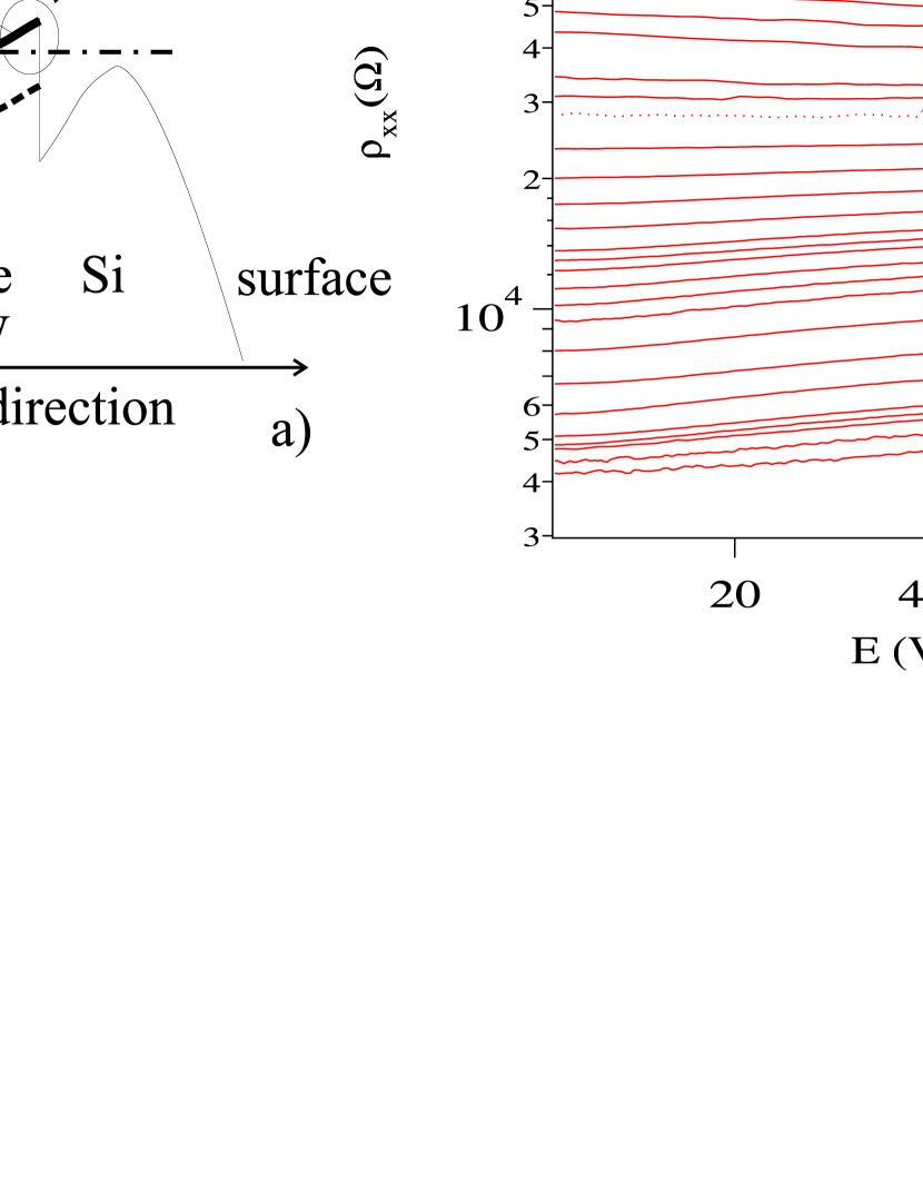
Current-voltage characteristics were measured with a DC-technique at . In Fig. 1b the differential resistivity is plotted as a function of electric field for different carrier concentrations. Plotting the differential resistivity makes undesired DC-offsets caused by our amplifier disappear and allows us to compare directly the different curves. At high carrier densities (low ), the behaviour is that of a metal: for large electric fields the resistivity increases. For the lowest carrier concentrations, the behaviour is instead insulating, with a lower resistance at higher E-fields. At a critical density a resistivity of () is observed, independent of the electric field. By plotting vs. for different values of the exponent and , it is possible to find a for which all the resistivity curves fall on one of two branches, one for the insulating () and one for the metallic region (). An example of such a plot is shown in Fig. 2, for . In this figure the overlap has been optimized for the metallic phase. Close to the critical point there is a symmetry between the two resistivity branches, but this is lost at higher fields, where the insulator traces no longer fall onto one scaling curve.
The transition can also be seen in the temperature dependence of . In Fig. 1c we show this for . The critical density, , is very close to that found in the electric field experiments. For densities close to the critical point, changes sign as the temperature is lowered. This makes the determination of the critical density less accurate than in the E-field scaling. For the temperature dependence it is possible to obtain scaling, by plotting vs. where the exponent is chosen such that the measured traces fall onto two separate scaling curves, with a reasonable symmetry between the two phases.
For a quantum phase transition the resistivity is expected to be a function of or , depending on whether the correlation lengths are controlled by the temperature or the electric field [6]. From the above stated dependence on E and T we see that the two exponents determined from E-field and temperature scaling, depend on the dynamical exponent and the correlation length exponent : and . Assuming the same functional form of the resistivity for the E-field and temperature, the two types of scaling behaviour can be mapped onto each other via with being a system dependent constant. For a strongly interacting 2D system is expected [6]. In order to test this we scale and on top of each other. In Fig. 2 is plotted against and , with a reasonable scaling behaviour for both curves. In the inset has been multiplied by a constant , which demonstrates the highly identical resistivity dependence on and in the metallic regime, and strongly supports . This gives a value for .
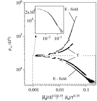

While is predicted to be equal to 1 [6], we are not aware of any predictions for the value of for the 2D MIT. The dependence suggests that the elctric field can be interpreted in terms of quantum fluctuations [6], but we can not exclude the possibility of a heating mechansim due to the electric field which could lead to the same dependence.
In our system the transition is found for , where is the mean free path as deduced from the mobility, and is the Fermi wave vector. This point also corresponds to a ratio between the Coulomb interaction and the Fermi energy, . The value of in the metallic region has been considered as evidence for the electron-electron interaction playing a major role [1].
In contrast to the Si MOSFET material system [8] in the present hole gases no resistivity increase with magnetic field applied parallel to the 2DHG is observed, and the E-field behaviour remains the same. This is quantified by fitting the resistivity to [7], with , where (see above), and and as –independent parameters. and are used as fitting parameters, whereas has been kept constant for all fits (). In Fig. 3, the energy gap vs. carrier density is shown for the case of zero field and a field applied parallel to the SiGe quantum well. There is no indication of any magnetic quenching of the energy gap. In the inset of Fig. 3, vs. is shown for and for , for two different carrier densities. Except for an overall increase in the resistivity, the behaviour remains essentially the same. The difference between the magnetic quenching of the transition in a Si MOSFET [8] and the present observation can be understood by considering the Zeeman effect in a SiGe 2 DHG. The carriers populate a heavy hole subband, with the characteristics , where is the total angular momentum. Due to the symmetry of this state, will be aligned perpendicular to the quantum well, and this arrangement is reinforced by the strain splitting, which further removes the lowest heavy hole state from the light hole states. Thus the total angular momentum feels an easy axis, and the magnetic energy will be dominated by the magnetic field component perpendicular to the quantum well (in order to break the LS coupling, a field of the order of would be needed). The lack of any influence on the metallic conduction by a parallel magnetic field, together with the breakdown of this phase in systems without an easy axis, supports the hypothesis that a spin related mechanism plays a key role for the MIT in 2 D.
In conclusion, -field and temperature scaling behaviour have been demonstrated for the MIT observed in a SiGe 2 DHG. Scaling plots lead to a dynamical exponent and a correlation length exponent . A magnetic field up to applied parallel to the interfaces does not quench the transition.
We wish to thank D. Bächle and T. Mezzacasa for assistance with
the
processing, and P. Studerus for help with the electronics. P.
Coleridge is
gratefully acknowledged for helpful discussions. This work was
supported by the
Schweizerischer Nationalfonds and MINAST.
References
- [1] S.V. Kravchenko, G.V. Kravchenko, J.E. Furneaux, V.M. Pudalov, and M. D’Iorio, Phys. Rev. B, 50 (1994) 8039; S.V. Kravchenko, D. Simonian, M.P. Sarachik, W. Mason, and J.E. Furneaux, Phys. Rev. Lett., 77 (1996) 4938.
- [2] P.T. Coleridge, R.L. Williams, Y. Feng, and P. Zawadzki, Phys. Rev. B, 56 (1997) 12764.
- [3] M.Y.Simmons, A.R. Hamilton, M. Pepper, E.H. Linfield, P.D. Rose, D.A. Ritchie, A.K. Savchenko, T.G. Griffiths, Phys. Rev. Lett., 80 (1998) 1292; Y. Hanein, U. Meirav, D. Shahar, C.C. Li, D.C. Tsui, H. Shtrikman, Phys. Rev. Lett., 80 (1998) 1288.
- [4] E. Ribeiro, R.D. Jäggi, T. Heinzel, K. Ensslin, G. Medeiros-Ribeiro, P.M. Petroff, Phys. Rev. Lett., 82 (1999) 996.
- [5] Y. Hanein, D. Shahar, J. Yoon, C. C. Li, D. C. Tsui, and Hadas Shtrikman, Phys. Rev. B, 58 (1998) R13338.
- [6] S.L. Sondhi, S.M. Girvin, J.P. Carini, and D. Shahar, Rev. Mod. Phys., 69 (1997) 315.
- [7] V.M. Pudalov, JETP Lett., 66 (1997) 175.
- [8] D. Simonian, S.V. Kravchenko, M.P. Sarachik, and V.M. Pudalov, Phys. Rev. Lett., 79 (1997) 2304.