[
Effect of Local Magnetic Moments on the Metallic Behavior in Two Dimensions
Abstract
The temperature dependence of conductivity in the metallic phase of a two-dimensional electron system in silicon has been studied for different concentrations of local magnetic moments. The local moments have been induced by disorder, and their number was varied using substrate bias. The data suggest that in the limit of the metallic behavior, as characterized by , is suppressed by an arbitrarily small amount of scattering by local magnetic moments.
pacs:
PACS Nos. 71.30.+h, 71.27.+a, 73.40.Qv]
A metal-insulator transition (MIT) has been observed recently in a variety of two-dimensional (2D) electron [1, 2, 3, 4] and hole [5, 6] systems but there is still no generally accepted microscopic description of the 2D metallic phase. Some of the relevant properties of the 2D metal include: (a) an increase of conductivity with decreasing temperature (i. e. ) for carrier densities ( – critical density); and (b) a suppression of the behavior by magnetic field [7]. The latter suggests the importance of the spin degrees of freedom, which can be probed further by studying the effect of local magnetic moments on the transport properties of the conduction electrons. Indeed, magnetic impurities have been used extensively over the last several decades to probe the properties of metals, and continue to be relevant today in attempts to understand heavy-fermion materials and high- superconductors [8]. In the experiment discussed below, the number of local moments is varied in a controlled way. We show that in the limit the behavior is suppressed by an arbitrarily small amount of scattering of the conduction electrons by disorder-induced local moments.
We present results obtained on a 2D electron system in Si metal-oxide-semiconductor field-effect transistors (MOSFETs). In such a device, the disorder is due to the oxide charge scattering (scattering by ionized impurities randomly distributed in the oxide within a few Å of the interface) and to the roughness of the Si-SiO2 interface [9]. For a fixed , it is possible to change the disorder by applying the substrate (back gate) bias . In particular, the reverse (negative) moves the electrons closer to the interface, which increases the disorder. It also increases the splitting between the subbands since the width of the triangular potential well at the interface is reduced by applying negative . Usually, only the lowest subband is occupied at low , giving rise to the 2D behavior. In sufficiently disordered samples, however, the band tails associated with the upper subbands [10] can be so long that some of their strongly localized states may be populated even at low , and act as additional scattering centers for 2D electrons. Clearly, the negative reduces this type of scattering by depopulating the upper subband. The effect of scattering by electrons localized deep in the tails of the upper subband was first observed as an enhancement of the mobility at low with negative [11], and was subsequently studied in more detail by other groups using different measurements and techniques [12]. More recently, we have used one negative value of to enhance (reduce the disorder) at intermediate values of , and observed the change from to for [2]. Here, however, we present a systematic study of this process as the disorder is varied using . We show clearly that the bare value of high (Drude) mobility is not sufficient to predict the sign and the magnitude of at low but rather that it is the type of the disorder that is relevant [13]. In particular, we show that scattering by electrons localized in the tail of the upper subband has a much more profound effect on than potential scattering due to oxide charges and surface roughness. This is attributed to spin flip scattering by electrons in localized states that are singly populated due to a strong on-site Coulomb repulsion, and act as local magnetic moments. Large on-site Coulomb interaction has been well documented in systems similar to ours, such as electrons in quantum dots [16], and other materials with strongly localized states [17]. For typical localization lengths of 100 Å in Si MOSFETs [9, 18], the on-site Coulomb repulsion is 10 meV. Therefore, such states will be singly occupied at low [9].
Our measurements were carried out on n-channel Si MOSFETs with the oxide charge density of cm-2, determined using standard techniques [9, 19]. Other details of the sample structure are given in Ref. [2]. For a fixed , was controlled by the gate voltage and determined in a standard fashion [9, 19]. was measured at temperatures K for of up to cm-2 and for –50 V+1 V. The effect of on at 4.2 K was found [14] to be consistent with earlier work and our interpretation. In particular, for (cm-2 is the density where reaches its maximum), an increase of is observed [14] with the negative as a result of the decreased scattering by local moments from the upper subband, and consistent with early work [11]. For , decreases with (negative) , consistent with the fact that surface roughness scattering is the dominant source of disorder in this range of [9]. This is a result of an increased proximity of the 2D electrons to the interface and, possibly, a reduction in scattering by local moments from the upper subband. The latter could be due to a smaller number of local moments being present in a sample at high (for a given ) because of an improved screening by 2D electrons. For sufficiently high negative ( V), the 4.2 K mobility decreases with for all , suggesting that the upper subband has been completely depopulated and that the further increase in leads only to increasing disorder due to potential scattering from roughness at the Si-SiO2 interface.
Fig. 1(a) shows some typical results for in the range as a function of . The metallic behavior, such
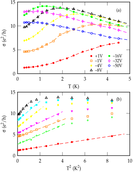
that , spreads out towards lower with the increasing negative , i. e. as the scattering by local moments is reduced, and it also spreads out towards higher values of (not shown). In other words, displays a maximum at , such that shifts to lower with the (negative) . As is increased beyond 35 V, the form of is no longer very sensitive to changes in even though the disorder due to potential scattering increases. In addition, by comparing the data for V and –1 V, for example, it is obvious that behavior is more pronounced ( is lower) when scattering by local moments is reduced even though the 4.2 K mobility is lower [13]. This demonstrates clearly the need to distinguish between different types of disorder, a fact that has been overlooked in some theoretically proposed phase diagrams [20, 21]. For , decreases with decreasing and, in fact, follows a form at the lowest [Fig. 1(b)]. Such is often considered to be a signature of local magnetic moments, and results from the Kondo effect [8]. Here it represents a direct evidence for the existence of local moments in our samples. A detailed study of this regime has been presented elsewhere [22]. Fig. 1(b) also shows that the range of () where local moments dominate transport becomes smaller as their number is reduced by increasing negative .
The position of the maximum in is shown in Fig. 2 for different values of as a function of the inverse subband
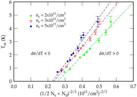
splitting ( is the depletion layer charge density, which increases with the reverse ) [9]. The metallic behavior with is observable at [see Fig. 1(a)]. For a given , extrapolates to zero for a finite value of the subband splitting. This value is slightly higher for higher , consistent with the fact that the number of local moments in the upper subband is also slightly higher (Fermi energy is higher) and, therefore, one needs to apply more in order to depopulate the upper subband. From the data shown in Fig. 2, it follows that goes to zero for V in agreement with the measurement of the 4.2 K mobility as discussed above. V corresponds to the subband splitting of the order of 30 meV [9]. The extent of the tail of the upper subband derived in this way is consistent with earlier work [12]. Our data, therefore, show that the 2D metal with can exist at only in the absence of scattering by disorder-induced local moments. This is similar to the behavior observed in a magnetic field [7], and consistent with some theoretical models [23, 24, 25, 26].
In the presence of scattering by local moments, is observable at , where , of course, can be arbitrarily small. For a fixed , for exhibits [2] all of the properties of a 2D MIT. Fig. 3 shows the values of and the (apparent) [27]

critical conductivity determined only from the data at , where scattering by local moments is not significant, as a function of . Both and increase monotonically with the reverse , i. e. with an increase in disorder due to potential scattering. The increase of and with disorder observed here on a single sample is in agreement with the same conclusion reached by comparing MOSFETs with different peak mobilities [28]. Fig. 3 inset shows the dependence of the critical exponents (– dynamic exponent, – correlation length exponent) on . was determined by scaling the data in the vicinity of , where [] [2, 27].
Fig. 4(a) shows for V for a small range of close to . Based on the analysis discussed above, we
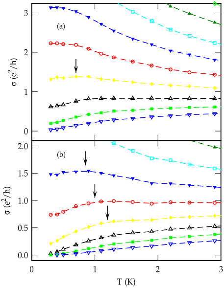
are confident that for this value of there are no local moments associated with the upper subband in the sample. Indeed, the curves do not exhibit a maximum in the measured range of , except possibly where shown in Fig. 4(a). Such a structure might, in fact, be due to local moments associated with the lowest subband. From the theoretical point of view, the possibility of disorder-induced local moment formation in strongly interacting electronic systems has been suggested since the early developments of the theory of interacting disordered systems [29, 24] and has been studied, subsequently, using different models [30]. In order to test this idea, we have increased to V, thus increasing the disorder, which is now due only to scattering by the oxide charges and the surface roughness. Fig. 4(b) shows that, for the same , the values of are reduced as expected for higher disorder. More importantly, we observe the appearance of the peak in for those for which it was clearly absent in Fig. 4(a). Also, a weak structure (peak) in for cm-2 has shifted to higher . This increase of , and the dependence of on as shown in Fig. 4(b), are qualitatively the same as what was observed by increasing the number of local moments associated with the upper subband. These results strongly suggest that an increase in the potential (non-magnetic) scattering has led to the formation of the (additional) local moments in the system. We have also observed similar peaks in in different Si MOSFETs at K but, without a systematic study such as this one, it would have been impossible to determine their origin. We speculate that local moments might exist in other materials as well but that the corresponding might be experimentally inaccessible in high-mobility devices.
Back gate bias was used recently in a 2D hole system [15] to study the effect of the spin-splitting due to the spin-orbit interaction and the inversion asymmetry of the confining potential [31]. It was found that the magnitude of the behavior was reduced as the spin-splitting decreased, i. e. as the confining potential became more symmetric. In our samples, we observe the opposite: the triangular confining potential becomes more symmetric with the application of the reverse , and that is exactly when the behavior appears. Therefore, even if the effect of the spin-orbit interaction exists in our samples, it does not drive the MIT.
The reverse also reduces the average spatial extent of the inversion layer charge density in the direction perpendicular to the interface (typically, Å) [9], leading to an increase of the effective Coulomb interaction [32]. Since ( – the average inter-carrier separation in units of the effective Bohr radius) is already fairly large () for close to (given in Fig. 3), we expect that the further increase in the Coulomb interaction for a fixed would only lead to an insulating behavior (see, e. g. Refs. [20, 21]) and not to the metallic behavior with , as observed. We conclude that the effect of on the effective Coulomb interaction is not the dominant effect in our samples.
Our study shows that the 2D metal with can exist in the limit only in the absence of scattering by local magnetic moments. Our results emphasize the key role of the spin degrees of freedom in the physics of the low density 2D electron system.
The authors are grateful to V. Dobrosavljević and A. B. Fowler for helpful discussions. This work was supported by NSF Grant No. DMR-9796339.
REFERENCES
- [1] S. V. Kravchenko, et al., Phys. Rev. B 50, 8039 (1994); S. V. Kravchenko, et al., Phys. Rev. B 51, 7038 (1995); S. V. Kravchenko, et al., Phys. Rev. Lett. 77, 4938 (1996).
- [2] D. Popović, A. B. Fowler, and S. Washburn, Phys. Rev. Lett. 79, 1543 (1997).
- [3] S. J. Papadakis, et al., Phys. Rev. B 57, R15068 (1998).
- [4] E. Ribeiro, et al., Phys. Rev. Lett. 82, 996 (1999); Y. Hanein, et al., preprint, cond-mat/9808251.
- [5] J. Lam, et al., Phys. Rev. B 56, R12741 (1997); P. T. Coleridge, et al., Phys. Rev. B 56, R12764 (1997).
- [6] Y. Hanein, et al., Phys. Rev. Lett. 80, 1288 (1998); M. Y. Simmons, et al., Phys. Rev. Lett. 80, 1292 (1998). (1998).
- [7] D. Simonian, et al., Phys. Rev. Lett. 79, 2304 (1997); V. M. Pudalov, et al., JETP Lett. 65, 932 (1997).
- [8] See, for example, A. C. Hewson, The Kondo Problem to Heavy Fermions (Cambridge University Press, Cambridge, England, 1993).
- [9] See T. Ando, A. B. Fowler, and F. Stern, Rev. Mod. Phys. 54, 437 (1982), and references therein.
- [10] Usually, this is a tail of the subband – the lowest subband associated with the four conduction band valleys with the light effective mass (0.190 ) perpendicular to the interface. See also Ref. [9].
- [11] A. B. Fowler, Phys. Rev. Lett. 34, 15 (1975).
- [12] A. Kastalsky, et al., Surf. Sci. 113, 153 (1982); S. Kawaji, et al., Surf. Sci. 196, 316 (1988); D. Popović, F. F. Fang, and P. J. Stiles, Sol. St. Comm. 68, 25 (1988).
- [13] This also explains the recent observation (Refs. [14] and [15]) that the metallic behavior in some samples is more pronounced (i. e. the magnitude of negative is larger) when the mobility is lower.
- [14] X. G. Feng, D. Popović, and S. Washburn, in the Proceedings of the 24th International Conference on the Physics of Semiconductors (CD-ROM version, World Scientific, Singapore, 1998).
- [15] S. J. Papadakis, et al., (unpublished).
- [16] See H. van Houten, C. W. J. Beenakker, and A. A. M. Staring, in Single Charge Tunneling: Coulomb Blockade Phenomena in Nanostructures, edited by H. Grabert and M. H. Devoret (Plenum Press, New York, 1992).
- [17] See, for example, D. Ephron, et al., Phys. Rev. Lett. 69, 3112 (1992) for work on amorphous Si.
- [18] G. Timp, et al., Phys. Rev. B 34, 8771 (1986).
- [19] D. Popović, A. B. Fowler, and P. J. Stiles, Phys. Rev. B 43, 4495 (1991).
- [20] S. Chakravarty, et al., preprint cond-mat/9805383 (1998).
- [21] J. S. Thakur, et al., Phys. Rev. B 59, R5280 (1999).
- [22] X. G. Feng, D. Popović, S. Washburn, and V. Dobrosavljević, preprint cond-mat/9903236 (1999).
- [23] C. Castellani, et al., Phys. Rev. B 57, R9381 (1998).
- [24] A. M. Finkel’stein, Sov. Phys. JETP 57, 97 (1983); Sov. Phys. JETP Lett. 40, 796 (1984); Z. Physik 56, 189 (1984).
- [25] C. Castellani, et al., Phys. Rev. B 30, 527 (1984).
- [26] Y. Takada, J. Phys. Soc. Jpn. 49, 1713 (1980); M. J. Kelly and W. Hanke, Phys. Rev. B 23, 112 (1981); P. Phillips, et al., Nature 395, 253 (1998); D. Belitz and T. R. Kirkpatrick, Phys. Rev. B 58, 8214 (1998).
- [27] Strictly speaking, with (N. J. Kim, D. Popović, and S. Washburn, preprint cond-mat/9809357); since this temperature dependence is so weak, appears to be constant at high enough .
- [28] V. M. Pudalov, et al., JETP Lett. 68, 442 (1998).
- [29] C. Castellani, et al., Phys. Rev. B 30, 1596 (1984).
- [30] M. Milovanović, et al., Phys. Rev. Lett. 63, 82 (1989); R. N. Bhatt and D. S. Fisher, Phys. Rev. Lett. 68, 3072 (1992); V. Dobrosavljević and G. Kotliar, Phys. Rev. Lett. 71, 3218 (1993); V. Dobrosavljević and G. Kotliar, Phys. Rev. B 50, 1430 (1994); A. Langenfeld and P. Wölfle, Ann. Physik 4, 43 (1995).
- [31] Yu. A. Bychkov and E. I. Rashba, JETP Lett. 39, 78 (1984).
- [32] F. C. Zhang and S. Das Sarma, Phys. Rev. B 33, 2903 (1986).