Infinite magnetoresistance of magnetic multilayers
Abstract
We examine transport properties of a magnetic superlattice with current perpendicular to the planes. In the limit that the phase-breaking and spin flip scattering lengths are greater than the system size, a multiple-scattering approach is used to calculate the 4-probe conductance. We show that by tuning the strength of tunnel barriers placed between the current and voltage probes giant magnetoresistance ratios of arbitrary strength and size are achievable.
pacs:
Pacs numbers: 72.10.Fk, 72.15.GdDuring the past few years advances in fabrication technology have enabled the production of precisely engineered mesoscopic superlattice (SL) structures, consisting of alternating magnetic and non-magnetic metallic layers, with well defined dimensions and interfaces. Exchange coupling of the magnetic layers through the non-magnetic material gives rise to antiferromagnetic (AF) alignment of adjacent magnetic layers. When such AF alignment is broken by applying a large magnetic field, a global ferromagnetic (F) configuration of the multilayer is achieved, and the resistance drops drastically [1, 2, 3, 4]. Such functional magnetic materials are the focus of substantial research both from a technological and fundamental viewpoint, having a wide range of applications in magneto-electronics [5], such as read/write heads for high density magnetic storage systems, and in the miniaturization of magnetic field sensors, such as solid state compasses [6]. All these applications require materials/geometries capable of giving a large signal (i.e. a large drop in resistance), and high sensitivity (so that only a small magnetic field required). Conventional materials, such as the 3 transition metal multilayers, show large GMR, but high magnetic fields are necessary to overcome the exchange coupling, making such systems unsuitable for most applications. For inhomogeneous multilayers based on polycrystalline alloys [6] much smaller fields are required, but show quite small drops in resistance. The half-metals such as CrO2, in principle can guarantee an infinite GMR [7, 8], but to date a GMR of only 50% has been measured in CrO2 powders at low temperature [9].
In this letter we argue that attention should also focus on the problem of optimising the scattering properties of a given structure and on the role of external probes. By tunning the scattering potential in a 4 - probe geometry we shall demonstrate a significant GMR enhancement can be achieved.
Transport properties of GMR structures are typically studied, when the current flows either in the plane of the layers (CIP) or perpendicular to the plane of the layers (CPP). In the CIP configuration the dimensions are macroscopic and 4 probe measurement techniques are used [10]. In contrast CPP measurements are usually carried out with 2 probes, using sophisticated techniques to measure the small resistances involved (). The CPP configuration is particularly interesting because it produces a larger GMR signal, with changes in resistance up to % [11, 12]. Remarkably however very little research has been conducted using 4 probe measurements on CPP geometries [13], despite the fact that the quantum nature of transport in such structures gives rise to unexpected phenomena, as detected in anisotropic magnetoresistance (AMR) systems of Co/Ni multilayers [14, 15].
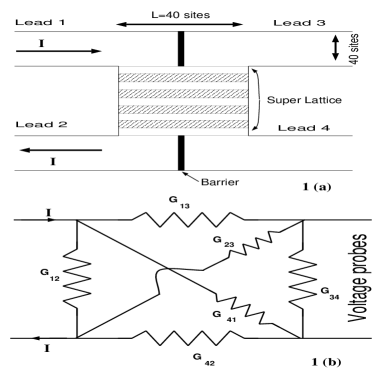
In this letter we consider a 4 probe CPP structure, and demonstrate that due to an inherent instability of 4 probe conductance measurements, an infinite magnetoresistance (IMR) is achievable. We use a general scattering approach to dc transport, developed to describe phase-coherent transport in dirty mesoscopic structures, and based on the fundamental current-voltage relations derived in [16]. For simplicity in this Letter, we focus on the conductance of the structure shown in Fig.1(a), which comprises a superlattice, with alternating normal and magnetic metal layers, in contact with four normal reservoirs at voltages ). The leads connecting the structure to reservoirs 1 and 2 carry a current , whereas leads 3 and 4 carry no current and hence form the voltage probes. The current/voltage leads are separated by an insulating barrier.
In what follows, we consider the zero-temperature, zero-bias limit in which the phase-breaking and spin-flip scattering lengths are greater than the dimensions of the system. In this limit, transport properties depend not only on the electronic structure of the magnetic multilayers, but also on the contacts with external reservoirs. This feature is embodied in a fundamental current - voltage relation due to Büttiker [16],
| (1) |
which relates the current from a normal reservoir to the reservoir voltages . The coefficients satisfy . In units of [16], and , where is the transmission coefficient from probe to probe , is the reflection coefficient in probe and is the number of open scattering channels in lead . As indicated in Fig. 1b, Eq.(1) can be viewed as an equivalent circuit representation of the phase coherent structure of Fig.1a. However the elements are correlated functionals of the scattering potential generated by contact with external leads, geometry and disorder, and therefore cannot be varied independently. Furthermore, as noted in [16] , where is the Hamiltonian of the system and therefore in the presence of a magnetic field, .
Setting and solving Eq.(1) for the conductance yields,
| (2) |
where is the determinant of the matrix obtained by removing the third row and column from the matrix of Eq.(1). In what follows we compute the GMR ratio () as [4]
| (3) |
where is the conductance for the minority (majority) spin in the F configuration, and is the conductance for both spins in the AF configuration.
In the F and AF configurations, the various transmission and reflection coefficients for the separate spins can be computed by solving the Schrödinger equation on a nearest neighbor tight-binding lattice of sites. In simple quasi one dimensional gemoetries involving only two probes, by combining an efficient recursive Green’s function approach with a material-specific s-p-d tight-binding Hamiltonian one can accurately predict the GMR ratio for a range of materials and layer thickneses [21]. For more complex geometries involving several probes, this is beyond the capabilities of currently available computing resources and therefore to demonstrate a generic enhancement of the GMR ratio, we analyze a tight binding model with a single degree of freedom per spin on each lattice site, as introduced in [17, 18]. Each lattice site is labeled by an index and possesses a spin degree of freedom , and the corresponding Schrödinger equation has the form
| (4) |
where sums over all neighbors of . The nearest neighbor hopping elements fix the band-width and determines the band-filling. The separate spin fluids are assigned a spin-dependent on-site energy . The parameters used in the present calculations are as follows: in the leads and non-magnetic regions of the SL and ; in the magnetic layers and () for spin up (down). Following [21] the hopping elements joining magnetic-normal sites are chosen to be the geometric mean of the hopping elements in the magnetic/normal regions.
The dc conductance (2) is determined by the multi-channel quantum mechanical scattering matrix, which in turn can be found from the Green’s function for a given structure. The numerical approach involves attaching the scattering region to crystalline semi-infinite leads, in which the Green’s functions are superpositions of plane waves, and then using Dyson’s equation to determine the total Green’s function [21]. Effectively this procedure requires the inversion of Hamiltonian describing the scatterer, which for the structure analyzed here is a matrix per spin degree of freedom. As we are only interested in the Green’s functions on the surface of the structure the inversion is carried out after the Hamiltonian has been renormalised in real space using an exact decimation technique [23].
As shown in Fig.1a the structure analyzed consists of four, crystalline semi-infinite leads each 40 sites wide. The superlattice consists of 5 non-magnetic layers alternating with 4 magnetic layers, each 8 sites wide and 40 sites long. The leads are separated by barriers, 2 sites wide and of strength . These barriers change the on-site energy in Eq.(4) to . Hence, varying the magnitude of alters the transmission and reflection coefficients of the current/voltage leads. For a barrier of width 2 sites, fig.2 shows the dependence on of the transmission coefficient per open channel, which as expected, decays exponentially with for large .
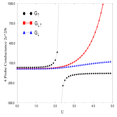
Fig.3 shows the dependence of , and on barrier strength. We see that and increase smoothly as is increased, whereas diverges for , and then returns to a negative constant. This divergence occurs as the transmission coefficient from lead 4 to lead 1 approaches the transmission coefficient from lead 4 to lead 2.
To gain physical insight into the origin of this divergence, we return to the equivalent circuit of fig.1b and consider the case of a symmetric structure, where = , , and Eq.(2) reduces to
| (5) |
From this expression we see that if then the 4 probe conductance will be negative and when , the conductance is infinite. Of course since the quantities are determined by the quantum mechanical scattering properties of the structure in figure 1, there is no guarantee that such a condition is achievable. The fact that we are able to demonstrate that this can occur in a realisable structure is a key result of this Letter.
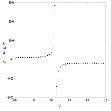
Fig.4 shows the dependence of the GMR ratio on barrier strength, calculated using Eq.(3). Due to the behavior of the majority spin state (), the GMR ratio increases with increasing , diverges for giving an IMR. Further increasing U causes the GMR ratio to return from - to a constant negative value, of around . We note that such negative GMR is not due to an intrinsic scattering asymmetry of the materials as measured in Ref.[19], but is due to the peculiar spin-dependent behavior of the 4 probe measurement. It is important to point out that the system we described is in principle tunable, for example by applying a gate electrode giving rise to the barrier potential U. Hence by changing the external gate potential, arbitrary GMR ratios may be obtained, using exactly the same principle as a Wheatstone bridge, despite the fact that the system described is fully quantum mechanical.
In conclusion, we have shown for the first time that due to an inherent instability in the 4-probe conductance of mesoscopic structures an infinite GMR ratio is realizable. To-date a great deal of effort has been aimed at optimizing the materials used in GMR devices. The above results suggest that geometry and external gating may be equally crucial in the race to obtain inexpensive magnetoresistive devices. This effect is a generic feature of the 4 probe geometry, and the use of a simple single-band tight-binding model is sufficient to demonstrate the possibility of IMR. Nevertheless more sophisticated material-specific tight-binding models [20, 21], or ab-initio calculations [22], will be needed to provide quantitative insights into real device characteristics.
Acknowledgments
The authors wish to thank P.wright, A. Volkov, R. Raimiondi and V. Falko for detailed discusions. This work is funded by the EPSRC and the E.U. TMR programme.
REFERENCES
- [1] M.N.Baibich, J.M.Broto, A.Fert, F.Nguyen Van Dau, F.Petroff, P.Etienne, G.Creuzet, A.Friederich, and J.Chazelas, Phys. Rev. Lett. 61, 2472 (1988)
- [2] G.Binasch, P.Grünberg, F.Sauerbach and W.Zinn, Phys. Rev. B 39, 4828 (1989)
- [3] J-Ph Ansermet, J. Cond. Mat. 10, 6027 (1998), and reference therein
- [4] M. A. M. Gijs and G. E. W. Bauer, Adv. Phys., 46, 285 (1997), and references therein.
- [5] Physics Today, Special Issue Apr. 1995, pag. 24
- [6] W. Clemens, H. A. M. van den Berg, G. Rupp, W. Schelter, M.Vieth, J. Wecker, J. Appl. Phys. 81, 4310 (1997)
- [7] A.M.Bratkovsky, Phys. Rev. B 56, 2344 (1997)
- [8] A.M.Bratkovsky, Appl. Phys. Lett. 72, 2334 (1998)
- [9] J. M. D. Coey, A. E. Berkowitz, Ll. Balcells, F. F. Putris, A. Barry, Phys. Rev. Lett. 80, 3815 (1998)
- [10] S. S. P. Parkin, Z. G. Li, D. J. Smith, Appl. Phys. Lett. 58, 2710 (1991)
- [11] W. P. Pratt, S.-F. Lee, J. M. Slaughter, R. Loloee, P. A. Schroeder and J. Bass, Phys. Rev. Lett. 66, 3060 (1991)
- [12] W. P. Pratt, S.-F. Lee, P. Holody, Q. Yang, R. Loloee, J. Bass, P. A. Schroeder, J. Magn. Magn. Mater. 126, 406 (1993)
- [13] M. A. M. Gijs, J. B. Giesbers, M. T, Johnson, J. B. F. Van de Stegge, H. H. J. Janssen, S. K. J. Lenczowski, R. J. M. Van de Veerdonk, W. J. M. de Jonge, J. Appl. Phys. 75, 6709 (1994)
- [14] De-Hua Han, Appl. Phys. Lett. 68, 2153 (1996)
- [15] C.Prados, D.Garcia, F.Lesmes, J.J.Freijo, A.Hernando Appl. Phys. Lett. 67, 718 (1995)
- [16] M. Büttiker, J.Res.Dev. 32, 317 (1988)
- [17] A. Oguri, Y. Asano and S. Maekaura, J. Phys Soc Jap 61 2652 (1992)
- [18] Y. Asano and S. Maekaura, Phys Rev B 48 6192 (1993)
- [19] S. Y. Hsu, A.Barthélémy, P. Holody, R. Loloee, P. A. Schroeder, A.Fert, Phys. Rev. Lett. 78, 2652 (1997)
- [20] E. Yu. Tsymbal, D. G. Pettifor, Phys. Rev. B 54, 15314 (1996)
- [21] S.Sanvito, C.J.Lambert, J.H.Jefferson, A.M.Bratkovsky, submitted to Phys.Rev.B (cond-mat/9808282)
- [22] K. M. Schep, P. J. Kelly, and G. E. W. Bauer, Phys. Rev. B 57, 8907 (1998)
- [23] C.J.Lambert and D. Weaire, Phys. Stat. Sol. (b) 101, 591 (1980)