Impurity effect on low-temperature polarisation of the charge-density-waves in o-TaS3
Abstract
The temperature dependence of the low-temperature dielectric response is
studied in o-TaS3 samples doped by Nb, Se, and Ni and for nominally pure
ones. It is found, that the low-temperature dielectric constant depends
anomalously on doping and is higher for doped crystals, whereas the
temperature dependence of the characteristic time of all samples follows
the activation law with nearly the same
activation energy K ( K). The observed behaviour is
inconsistent with all available explanations of the low-temperature
dielectric anomaly.
pacs:
PACs numbers: 71.45.Lr, 72.15.Nj, 64.60.FrKeywords: charge-density waves, dielectric relaxation, pinning, glass transition, creep
I Introduction
Quasi-one dimensional conductors like TaS3, K0.3MoO3 etc. are well known physical systems which undergo spontaneous structural transition into a low-temperature ordered state, where one of the most widely studied electronic crystal - the charge-density waves (CDWs) - is formed [1]. Similarity between the physical properties of the CDW conductors, Wigner crystals, vortex lattices in superconductors, together with the specific possibility of measurements of extremely small displacements of the electronic crystal, that in the case of the CDW is associated with extremely high dielectric constant up to , makes the CDW conductors one of the most convenient model system for investigation of the collective response to an external force.
In quasi-one dimensional conductors at an electric field high enough to overcome the CDW-impurity interaction the CDW starts to slide providing a contribution in nonlinear conduction. At relatively small electric fields the CDW is pinned by impurities, and its response to an electric field may provide an information on CDW-impurity interaction, as well as on the CDW state itself. In the recent years the interest to dielectric properties of the CDW conductors have been revived because of observation of the low-temperature anomaly of their for low frequencies Hz [2, 3, 4, 5, 6]. The origin of this anomaly remains to be the subject of intensive study and discussion [2, 3, 4, 5, 6, 7, 8].
Many experimental facts show that the CDW at sufficiently low temperatures is characterised by ”glassy” behaviour (see [9] and references therein) related to the existence of metastable states in the CDW system. In particular, the rough free energy landscape caused by pinning of the CDW leads to a continuous relaxation times spectrum that reveals itself in a long-time logarithmic relaxation of polarisation. In the framework of this “glassy” approach the temperature maximum in marks the critical slowing down of the CDW kinetics, when the system goes through a temperature-dependent characteristic time into a glassy state [2], which in the case of TaS3 was recognised as a disorder-induced glassy state [5, 6].
Alternative explanations of the low-temperature anomaly were given recently [7, 8]. On the first hand, Volkov [7] analysed the screening effects on a deformed CDW presented in the form of a periodic chain of phase solitons pinned by impurities. It was shown, that the characteristic time of the dielectric response of such a system follows an activation law. In the framework of this approach the activation energy of corresponds to the activation energy of the linear conduction, in agreement with the experimental data for K0.3MoO3 [2, 3, 4], (TaSe4)2I [10] and TaS3 at K [11, 12]. Note that for these materials, as well as for all known CDW materials, the dielectric constant decreases with increasing impurity concentration.
On the other hand, Brazovskii and Larkin [8] considered a phenomenological model of pinning, taking into account both local and collective types of pinning. It was shown that the characteristic time of the dielectric response of the pinned CDW follows an activation (in the case of a single pinning energy) or close to activation law (in the case of a distribution of the pinning energy) with the activation energy close to the pinning energy. The dielectric constant also decreases with increasing impurity concentration.
So the question on the origin of the low-temperature CDW polarisation anomaly remains to be open. At the same time, there is a way to distinguish experimentally between the explanations given above. For this purpose it is necessary to study the characteristic time, , and the dielectric constant, , as a function of the temperature, impurity concentration, , and their chemical type. If the maximum of the dielectric response is due to the disorder-induced glass transition [5, 6], the characteristic time increases with increasing impurity concentration . If the maximum is related to the screening mechanism [7], has the same activation energy as the screening carrier concentration (i.e. as the linear conduction). If the maximum is related to the pinning energy, the activation energy depends on a chemical type of dominating doping impurity, but is independent of their concentration. In all cases [2, 3, 4, 5, 6, 7, 8] the dielectric constant decreases with increase of impurity concentration.
In this paper we present results of the real-time low-temperature polarisation measurements of o-TaS3 doped by Nb, Ni, and Se, as well as for pure one. The measurements were carried out over the time interval from s to s in the temperature range 1.6-32 K. Our results show that the characteristic time follows the activation law with the activation energy independent of the doping element and its concentration, whereas the activation energy of the linear conduction varies within a factor 2. It is also found that the dielectric constant is higher for impure crystals. Our results are therefore inconsistent with all available explanations of the low-temperature dielectric anomaly and indicate that there are subgap excitations of the CDW mediating its low-temperature polarisation.
II Experimental
A real-time relaxation technique is appropriate to reveal the characteristics of the transport properties of the CDW and the low-frequency CDW excitations [2, 13, 14]. The time-domain measurements are free from the integral effects inherent to the frequency-domain technique in case of presence of internal interactions in the system [15]. We studied the dielectric response of o-TaS3 samples that arises during the application of an alternating-sign periodic train of voltage pulses (see inset in Fig. 1). Unlike the earlier measurements on the blue bronzes [2, 13] the polarisation charge was measured as a function of time after switching the polarisation voltage across the sample, , to its zero value. The curves were averaged over a large number of pulses (order of 100). Such zero voltage measurements allows us to get rid of the ohmic contribution of thermally activated quasi-particles, that is essential at long times and high temperatures. For the measurements we have used a hand-made integrator on the base of LMC6001 ultra-low input current amplifier. The low-frequency noise of the apparatus is of the order of A/ (at 1 kHz).
In addition, to compare the time-domain technique with frequency-domain technique we undertook measurements of real and imaginary parts of AC conduction in a frequency range 10 Hz - 10 kHz with using SR530 lock-in amplifier as a phase-sensitive detector.
o-Ta3 crystals as well as bundles originating from two different sources were investigated. Three batches were prepared at the Switzerland University and was kindly supplied to us by Dr. F. Levy. Other ones were prepared by us in IRE RAS (Moscow, Russia). The contacts to the samples were cold soldered 50-m In wires. The samples characteristics are briefly summarised in Table I.
| Sample | Nominal | ||||||
|---|---|---|---|---|---|---|---|
| Impurity Content | K | V/cm | K | K | K | ||
| 1a,b | pure | 221 | 0.4 | 400 | 420 | ||
| 2a,b | pure | 221 | 0.4 | 456 | |||
| 3c | pure | 220 | 1.4 | 360 | 437 | ||
| 4c | 0.2%Nb | 205 | 370 | 440 | |||
| 5c | 0.5%Nb | 202 | 476 | ||||
| 6b | 5%Ni | 219 | ‡ | 370 | 395 | ||
| 7b | 1%Se | 212 | 5 | 260 | 446 |
aSamples from the same batch.
bSamples prepared in IRE RAS (Moscow, Russia).
cSamples prepared in the Institut de Physique Appliquee (Lausanne,
Switzerland).
The dielectric constant was calculated as where is the length and is the
cross-sectional area of a sample.
‡I-V curves are nonlinear and have no threshold.
III Results
First of all we got sets of polarisation charge vs. polarisation pulse amplitude dependencies to find the linear response region. A voltage corresponding to this region for all temperatures was chosen for further detailed study of the response over entire temperature range. The results presented below corresponds to the linear response region.
The curves obtained at a fixed polarisation pulse duration are well reproducible. Comparing the curves measured for various we have detected a weak dependence of on different , like it was observed recently in K0.3MoO3 [16]. It has been checked up that the results reported here are not affected by this observed dependence and correspond to the infinite duration of the polarisation pulse.
Fig. 1(a) demonstrates a typical set of curves for pure and doped TaS3 samples. The relaxation of the polarisation is nonexponential; it continues to the longest times at which measurements were carried out.

For all samples at temperatures above approximately K we have observe a region with a comparatively rapid growth of with time. This relaxation mode gives a sharp maximum on a logarithmic derivative of the polarisation (Fig. 1(b)) indicating passing of the temperature-dependent characteristic time; in agreement with earlier studies [2, 3, 4, 5, 6, 14].
Fig. 1(b) shows the respective set of the logarithmic derivative of the relaxation curves, . The characteristic time, , is determined as a time corresponding to the maximum of the derivatives.
Fig. 2 shows typical temperature dependencies of the characteristic time of a pure and two doped samples. The high-temperature part of dependence ( K) can be fitted by the activation law with the activation energies K. The values of the crossover temperature , as well as the activation energies , are remarkably nearly the same for all samples (within 10% experimental error), i.e. they are independent of a crystal purity (see Table I). Moreover, the relaxation time at a fixed temperature does not correlate to neither type nor nominal concentration of the impurities in the studied samples. For example, doping by Nb increases K from s (sample 3) to s (sample 4) and s (sample 5), whereas doping by Ni decreases it down to s (sample 6) with respect to the most pure crystals 1-3.
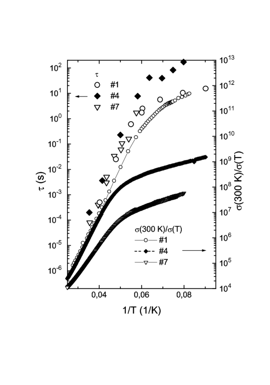
We also observed another branch of dependence. Note that the heights of maximums of curves (Fig. 1(b)) are approximately the same at K, but decrease rapidly at K. Similarly, the slope of vs. curve at is roughly by factor 4 lower that at . This indicates that there is a change of the relaxation mechanisms around . Suggesting the activation law for the low-temperature part of one gets the estimate for the activation energy around K depending on doping impurity.
In addition, measurements of the DC linear conduction temperature variation were carried out for the same samples for the temperature range K. Fragments of vs. curves are shown in Fig. 2. A region of the activation dependence, , is observed above 20 K, in agreement with the results of earlier studies. Note that while the slopes of curves are very close to each other, the slopes of curves are different. The respective set of demonstrates their distinction from (See Table I).
Direct measurements of the dielectric constant has shown that of impure crystals is higher than of pure ones (see Table I). To verify this result we also measured the ratio ( is an imaginary part of the AC conduction) which is independent of the geometrical factors. As , is practically independent of impurity concentration, this ratio can be considered as a measure of the low-temperature dielectric constant. And again, it was found that is higher for impure crystals than for pure ones. That reflects growth of the low-temperature with increase of impurity concentration. Note that this unusual low-temperature behaviour of is opposite to the high-temperature behaviour corresponding to the relation well-known for the high-temperature region [17].
IV Discussion
As was noted above, absence of any correlation between the characteristic time and impurity content does not support the earlier suggestion [5, 6] on the disorder-induced glass transition as a mechanism responsible for the low-temperature dielectric anomaly.
In principle, the strong-pinning model [8] may provide impurity independent activation energy for the relaxation time. Namely, in the original model [8] the depinning barrier height depends on the pinning potential and may be arbitrary large. One should expect, however, that when the pinning potential exceeds some critical value, a new alternative channel for depinning of the CDW appears. For example, depinning of the CDW may occur through a suppression of the order parameter and local phase slip, rather than through further shift of the continuous CDW. The respective energy barrier depends mostly on parameters of the CDW itself rather than on its interaction with impurity. Nevertheless, the strong-pinning model [8] predicts qualitatively different dependencies of the dielectric constant on the impurity concentration than it was observed. Namely, it gives , where and are the weak and strong-pinning components respectively. At both components are expected to decrease with growing impurity concentration [8], the value of should be lower for doped crystals. In contrast, our experimental data clearly indicate growth of with increasing (see Table I). So the strong-pinning model [8] is inconsistent with the data.
As was noted above, the screening model [7] is consistent with the high-temperature dielectric anomaly obseved in K0.3MoO3[2, 3, 4], (TaSe4)2I [10] and TaS3 [11, 12] at , where CDW deformations are screened by normal carriers exited over the Peierls gap. To apply similar explanation to the low-temperature anomaly in TaS3 one needs to suggest existence of screening carriers with the activation energy around 400 K [18]. However, the present version of the screening theory [7] can hardly account for the opposite relations between and for high- (decrease of with ) and low-temperature ranges (increase of with ).
So neither of available explanations of the low-temperature dielectric anomaly of TaS3 is consistent with the actual dependencies of and . The most surprising result is growth of the dielectric constant with increase of impurity concentration (see Table I). Note, such a behaviour may reflect the decrease of the pinning energy per the phase-correlation volume with growth of : in the weak-pinning case (see e.g. Ref. [19] and references therein). Thus growths of both the low-temperature linear DC conduction observed earlier [20] and AC conduction reported here with increase of the impurity concentration are consistent with general expectations for creeping of weakly pinned CDW. Additional contribution to may also come from increase of CDW dislocation density with increase of [21].
Another surprising result is independence of on impurity type and concentration. This result indicates the existence of low-energy excitations in TaS3 that mediate the relaxation process. Though possible contribution of such excitations into low-temperature transport properties of TaS3 was broadly discussed earlier [18], no their contribution into the low-temperature conduction was observed in the present measurements.
In conclusion, the characteristic time of low-temperature polarisation of TaS3 is found to follow the activation law with the activation energy K independent of the dominant impurity and its concentration. In addition, the low-temperature dielectric constant of doped samples is found to be higher then of pure ones. The observed behaviour is inconsistent with all earlier suggested explanations of the low-temperature dielectric anomaly and implies existence of low-energy excitations having the activation energy 400 K and mediating the polarisation process.
V Acknowledgments
We are grateful to K. Biljaković, S. Brazovskii and A.F. Volkov for many useful discussions, and F. Levy for supplying some samples of o-TaS3. This work was supported by RFBR grants 97-02-17751, 98-02-16667, 98-02-22061, by MNTP ”Physics of Solid-State Nanostructures” (grant 97-1052), and by C.N.R.S. through jumelage 19 between C.R.T.B.T. and IRE RAS.
REFERENCES
- [1] For a review of physical properties of electronic crystals see: “Proceedings of the International Workshop on Electronic Crystals” ECRYS’93, Edited by S. Brazovskii and P. Monceau, J. de Physique IV, C2 (1993).
- [2] G. Kriza and G. Mihaly, Phys. Rev. Lett. 56 (1986) 2529.
- [3] G. Kriza, Y. Kim, A. Belaznay, and G. Mihaly, Solid State Commun., 79, 811 (1991).
- [4] J. Yang and N.P. Ong, Phys. Rev. B 44, 7912 (1991).
- [5] F. Ya. Nad’ and P. Monceau, Solid State Commun. 87, 13 (1993).
- [6] F. Ya. Nad’ and P. Monceau, Phys. Rev. B 51 (1995) 2052.
- [7] A. F. Volkov, Phys. Lett. A. 182 (1993) 433.
- [8] A. Larkin and S. Brazovskii, Solid State Commun. 93 (1995) 275.
- [9] K. Biljaković, in ”Phase Transitions and Relaxation in Systems with Competing energy Scales”, NATO Advanced Study Institute, ed. T. Riste and D. Sherrington, Kluwer Acad. Publ (1993) 339.
- [10] R.J. Cava, P. Littlewood, R. M. Felming, R.G. Dumn and E. A. Rietman, Phys. Rev. B, 33, 2439 (1985).
- [11] R. J. Cava, R. M. Felming, R.G. Dumn and E. A. Rietman, Phys. Rev. B, 31, 8325 (1986). Note that the activation energy 400 K mentioned in the text is actually around 800 K.
- [12] D. Starešinić, K. Biljaković, K. Hosseini, W. Brütting, H. Berger and F.Lévy, to be published.
- [13] L. Mihaly and G. Y. Tessema, Phys. Rev. B 33 (1986) 5858.
- [14] N. I. Baklanov and S. V. Zaitsev-Zotov, Pis’ma JETP 61 (1995) 656.
- [15] Dielectric relaxation in Solids, Ed. J. Harrison, Springer Verlag, Berlin (1983).
- [16] A. Beleznay, R. Gaal, and G. Mihaly, in [1], p.357.
- [17] W.W. Fuller, G. Grüner, P.M. Chaikin and N.P. Ong, Phys. Rev. B 23, 6259 (1981); A. Zettl, C.M. Jackson, and G. Grüner, Phys. Rev B, 26, 5773 (1982).
- [18] F.Ya. Nad’, in “Charge-density waves in solids”, Eds. G. Hutiray and J. Solyom, Springer Verlag, Berlin (1985), p. 286.
- [19] J. McCarten, D.A. DiCarlo, P.A. Maher, T.L. Adelman, and R.E. Thorne, Phys. Rev. B 46, 4456 (1992).
- [20] S.V. Zaitsev-Zotov, G. Remenyi and P. Monceau, Phys. Rev. B. 56, 6388 (1997).
- [21] Note that in TaS3 the threshold field for the onset of sliding of the CDW growths exponentially with lowering temperature. So one can expect that at sufficiently low temperatures nucleation of CDW dislocations reducing the CDW strain is energetically favourable. As a result, the CDW gets additional degree of freedom and may be more polarisable than a rigid CDW without dislocations.