Shot noise suppression in multimode ballistic Fermi conductors
Abstract
We have derived a general formula describing current noise in multimode ballistic channels connecting source and drain electrodes with Fermi electron gas. In particular (at ), the expression describes the nonequilibrium ”shot” noise, which may be suppressed by both Fermi correlations and space charge screening. The general formula has been applied to an approximate model of a 2D nanoscale, ballistic MOSFET. At large negative gate voltages, when the density of electrons in the channel is small, shot noise spectral density approaches the Schottky value , where is the average current. However, at positive gate voltages, when the maximum potential energy in the channel is below the Fermi level of the electron source, the noise can be at least an order of magnitude smaller than the Schottky value, mostly due to Fermi effects.
Nonequilibrium current fluctuations (”shot noise”) in ballistic conductors have been studied extensively in recent years both theoretically[1, 2, 3, 4] and experimentally[5, 6, 7, 8, 9] (see also Ref. [10]). All these works focused on the suppression of noise by Fermi correlations, which is especially strong when the channel transparency is close to 1. In order to observe this suppression, the experimental studies were invariably performed in a ”quantum point contact” geometry, i.e., within conductors with a small number of quantum channels, at temperatures much lower than the energy separation between those channels. (The case of noise in multimode ballistic Fermi systems did not attract that much attention.)
However, shot noise at ballistic transport may also be suppressed by Coulomb interactions of an electron with the space charge of other ballistic electrons. For nondegenerate, Boltzmann electron gas this effect was well studied long ago, mostly in the context of vacuum tube noise – see, e.g., Ref. [11] (See also recent Monte Carlo studies, Ref. [12]). To the best of our knowledge these studies have never been extended to the degenerate, Fermi systems. Such a study is of particular importance for at least two reasons.
From the fundamental point of view one should wonder whether the Fermi correlations may have a strong effect on the properties of wide, multichannel ballistic conductors. As for Coulomb correlations, it can be argued that its effect on the noise should be regarded as a much more accessible manifestation of electron-electron interactions than in more exotic phenomena, e.g., charge density waves.[4] In addition, it is important to understand the difference between nonequilibrium fluctuations in ballistic and diffusive Fermi systems. In the latter case, noise originates from scattering inside the conductor,[13, 14, 15] while in the former case its origin is the randomness of electron emission from the source.
From the point of view of possible applications, the continuing reduction of channel length of field-effect transistors will eventually but inevitably lead to devices with ballistic transport of electrons. A recent approximate analysis of such transistors has shown that they may retain high performance all the way down to 5 nm.[16] Such nanoscale MOSFETs may be used, in particular, as sense preamplifiers in ultradense nonvolatile memories.[17, 18] For these applications, the shot noise suppression is of principal importance because it determines how many single-bit memory cells may be served by one second-level sense amplifier, a number which may strongly affect the final memory density.
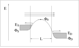
The objective of this work is to consider the interplay of the two mechanisms of shot noise suppression in a broad (multimode) system with the ballistic transfer of electrons from emitter to collector (Fig. 1). These electrodes are assumed to be in thermal equilibrium; in particular this means that the collector totally absorbs the incident electrons. (We will revisit this assumption at the end of the paper.) The potential energy profile between source and drain, and in particular its maximum , may be affected by the space charge of ballistic electrons. The charge density is determined, in turn, by the emitted current.[16]
In order to find the low-frequency shot noise in the device we start with the basic expression for the spectral density of fluctuations of current of electrons emitted by the source electrode at some interval of the total energy :[2, 3, 19]
| (2) | |||||
Here and are the electron distribution functions on the left and right hand sides of the interface between the source electrode and the conductor, respectively. is the mode transmission matrix across the interface, and the trace is taken over all the transmission modes with energy . The assumption of absorptive electrodes implies that the eigenvalues of are all equal to 1. This, together with conservation of transversal momentum, allows us to change the argument from the total energy to the longitudinal energy , and write Eq. (2) as
| (3) |
with
| (4) |
where
| (5) |
is the occupancy of transversal modes [ is the density of these modes], and with
| (6) |
A similar expression is valid for the intensity of electron emission from the second electrode (”drain”).
In our case of substantial Coulomb interaction between the ballistic electrons and space charge, we should recalculate fluctuations and into those of the total current . The general relation between these fluctuations may be written as follows [we take the direction of to be from drain to source],[11]
| (7) |
where are the potentials deep inside the source and drain, respectively (Fig. 1) and factors describe the space charge screening effect. In the limit , where is the ballistic time of flight, these factors may be calculated quasi-statically. In our model, with the source-drain voltage fixed in time (, are the Fermi energies in the source and drain, respectively), current is uniquely determined by This is why we can write:
| (8) |
with the upper (lower) sign used for (). In Eq. (8), the terms with derivatives describe the effect of the emission current fluctuation on the total current fluctuation via that of the local density of electrons, which in turn affects the potential barrier shape (and through the Poisson equation. The unity in the second line of Eq. (8) is due to the direct contribution of to Now, to calculate we combine Eqs. (2, 3, 7, 8) and take into account the statistical independence of sources and at different energies. As a result, we get
| (9) | |||
| (10) | |||
| (11) | |||
| (12) |
where , are the total source and drain currents at all energies below , respectively. This equation is the main result of our work. It describes the shot noise suppression via both the Fermi statistics of the emitted electrons (factors ) and their electrostatic interaction with space charge (factors with derivatives).
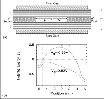
In order to evaluate the relative importance of these two suppression factors, we have applied Eq. (9) to a simple model of a nanoscale, ballistic, dual-gate MOSFET studied in Ref. [16] (Fig. 2a). This device consists of a thin layer of semiconductor with 2D electron gas embedded between two gates biased with equal voltages . The semiconductor is heavily doped everywhere except in a strip of length which forms the ballistic channel. Under certain conditions[16] the potential profile can be found from the effective 1D Poisson equation
| (13) |
where , and are the semiconductor thickness and the total distance between the gate electrodes, respectively, and , are the dielectric constants of the semiconductor and the insulator, respectively. The simple equation (13), together with the assumption of thermal equilibrium in source and drain, makes possible a semi-analytic scheme for finding all the quantities of interest. In that scheme the calculation starts with fixing while , , and are calculated by simple integration, enabling the final calculation of and for any by numerical interpolation. Figure 2(b) shows the calculated potential energy profile for large positive and negative gate voltages , for a device with the following parameters: nm, nm, nm, , , and donor density in the source and drain . (With the effective electron mass of 0.2 , the latter parameter means that the Fermi energy in the electrodes is close to 0.3 eV.) This parameter set corresponds to a Si MOSFET with SiO2 gate oxide, optimized for dc transport properties.[16]
Within the calculation scheme outlined above, the derivatives participating in Eq. (9) may be found as
| (14) |
Figure 3 shows the results of our calculations of the device noise for the parameter set specified above. (The results are qualitatively the same for any between 5 and 15 nm.) At negative gate voltages, when is substantially above , current noise is very close to the Schottky value ; however at positive gate voltages the noise may be suppressed by at least one order of magnitude.
Figure 4 assists the interpretation of this result by showing the factors participating in the first two integrals of Eq. (9), at two different gate voltages. Dotted lines represent the Fermi factor which is concentrated around the Fermi level of the source. The electrostatic term (dashed lines) peaks at due to the fact that electrons with this energy virtually stop near the maximum of the potential profile: . As a result, the corresponding change in charge density, is very large, and strongly affects the potential distribution.


At high negative gate voltages [Fig. 4(a)] the Coulomb interaction factor is very small, since the electron density in the channel is exponentially small and the space charge effects are negligible. Also, since is well above the Fermi level, the Fermi factor equals just . This factor gives equal contributions into the dc current and noise, and so the shot noise has its full, classical Schottky value. Another way to express the latter fact is to say that at negative gate voltages the conduction is due to electrons at the upper, Boltzmann tail of the Fermi distribution, and degeneracy effects are negligible.
At high positive gate voltage when [Fig. 4(b)], the space charge screening factor is rather moderate () for energies within the interval responsible for most of the current transfer. The reasons for this weak interaction are twofold. First, because of electron degeneracy, depends only algebraically on (in contrast to the exponential dependence in the nondegenerate case) so the derivative in Eq. (8) is relatively small. Second, the localized character of the electrostatic interaction, limited by the exponential cutoff at distances of the order of [see Eq. (13)] means that the derivative is small. On the other hand, in this open-channel regime, the Fermi suppression of noise is much larger, because the noise intensity is multiplied by the small term while the current is not. Physically this means that while the current is mostly due to all electrons within the interval , most of these electrons come from far below the Fermi energy and are “noiseless”.
Thus, though the device studied in this work is in some sense a Fermi analog of the classical vacuum tube, its degeneracy and its specific electrostatics (the exponential cutoff of Coulomb interactions of ballistic electrons due to the close proximity of the gates to the channel) reduce the space charge effects. The Fermi suppression of the shot noise, however, is quite strong. This result is very encouraging from the point of view of applications, but it may only be considered as preliminary.
In fact, the simple model of a ballistic MOSFET employed for the concrete calculations in this work (and used also in Ref. [16]) is somewhat self-contradictory. On one hand, in this model the source, channel, and drain are all described by the same Poisson equation (13). This implies that not only the channel but also source and drain are 2DEG sheets. On the other hand, the model assumes perfectly absorptive boundary conditions at the contact-to-channel interfaces, implying that the 2DEG in the contacts remains in thermal equilibrium. This assumption can be easily justified in geometries where the contacts are bulk (3D), or are made from a material with a much higher density of states.[20] Strictly speaking, this is not true in our model, if electron scattering in the contacts obeys the usual hierarchy: elastic scattering events are more frequent than inelastic ones. In fact, in this case a fraction of ”hot” (nonequilibrium) ballistic electrons entering the drain will be elastically scattered back to the channel before they have a chance to thermalize with the lattice. Thus in order to be realistic for usual devices (including the Si-based, room-temperature MOSFETs), the model needs to be refined. We believe, however, that such a modification will not change the results significantly.
In summary, we have derived a general equation (9) for shot noise in a multimode ballistic channel between electrodes in thermal equilibrium, which describes the noise suppression due to both Fermi correlations of ballistic electrons and their Coulomb interactions with space charge. Application of this general result to an approximate model of a ballistic MOSFET shows that at positive gate voltages the shot noise may be suppressed by more than an order of magnitude, mostly because of Fermi correlations. Our plans are to verify this result using more realistic MOSFET models.
We are grateful to P. Solomon for useful discussions and the opportunity to read his manuscript prior to publication. The work was supported in part by AME program of ONR/DARPA.
REFERENCES
- [1] V. A. Khlus, Zh. Eksp. Teor. Fiz. 93, 2179 (1987) [Sov. Phys. JETP 66, 1243 (1987)].
- [2] G. B. Lesovik, Pis’ma Zh. Eksp. Teor. Fiz. 49, 513 (1989) [JETP Lett. 49, 592 (1989)].
- [3] M. Buttiker, Phys. Rev. Lett. 65, 2901 (1990); Phys. Rev. B 46, 12485 (1992).
- [4] R. Landauer and Th. Martin, Physica B 175, 167 (1991); Th. Martin and R. Landauer, Phys. Rev. B 45, 1742 (1992).
- [5] Y. P. Li, D. C. Tsui, J. J. Heremans, J. A. Simmons, and G. W. Weimann, Appl. Phys. Lett. 57, 774 (1990);
- [6] M. Reznikov, M. Heiblum, H. Shtrikman, and D. Mahalu, Phys. Rev. Lett. 75, 3340 (1995).
- [7] A. Kumar, I. Saminadayar, D. C. Glattli, Y. Jin, and B. Etienne, Phys. Rev. Lett. 76, 2778 (1996).
- [8] C. Kurdak, C.-J. Chen, D. C. Tsui, J. P. Lu, M. Shayegan, S. Parihar, and S. A. Lyon, Surface Sci. 361/362, 705 (1996).
- [9] H. E. van der Brom and J. M. van Ruitenbeek, preprint cond-mat/9810276.
- [10] For a general review of mesoscopic ballistic transport see C. W. J. Beenakker and H. van Houten, Solid State Phys. 44, 1 (1991) and Y. Imry, Introduction to Mesoscopic Physics (Oxford, New York, 1997).
- [11] A. van der Ziel, Noise (Prentice-Hall, Englewood Cliffs, N.J., 1954).
- [12] T. Gonzalez, O. M. Bulashenko, J. Mateos, D. Prado, and L. Reggiani, Phys. Rev. B 56, 6424 (1997); O. M. Bulashenko, J. Mateos, D. Prado, T. Gonzalez, L. Reggiani, and J. M. Rubi, Phys. Rev. B 57, 1366 (1998).
- [13] C. W. J. Beenakker and M. Büttiker, Phys. Rev. B 46, 1889 (1992).
- [14] K. E. Nagaev, Phys. Lett. A 169, 103 (1992).
- [15] Y. Naveh, D. V. Averin, and K. K. Likharev, Phys. Rev. Lett. 79, 3482 (1997); Phys. Rev. B, in press.
- [16] F. G. Pikus and K. K. Likharev, Appl. Phys. Lett. 71, 3661 (1997).
- [17] Nonvolatile Semiconductor Memory Technology, ed. by W. D. Brown and J. E. Brewer (IEEE Press, New York, 1998).
- [18] K. K. Likharev, Appl. Phys. Lett. 73, 2137 (1998).
- [19] Sh. Kogan, Electronic noise and fluctuations in solids (Cambridge, Cambridge, 1996), chapter 5.
- [20] See, e.g., P. M. Solomon, “On Contacts to Small Semiconductor Devices”, unpublished. Similar restrictions of the ”rigid” boundary conditions have also been repeatedly discussed in theories of superconductor weak links – see, e.g., K. Likharev, Rev. Mod. Phys. 51, 101 (1979).