Excess conductance in normal-metal/superconductor junctions
Abstract
The current-voltage characteristics of Au//Pb tunnel junctions exhibit peculiar zero-bias anomalies. At low temperatures the zero-bias resistance attains values that are smaller than the normal state resistance by a factor that often exceeds 2. The width of this anomaly increases with the thickness of the layer. The possibility that these features arise from the nature of the barrier being an Anderson insulator is discussed.
pacs:
PACS numbers:73.40.GK 72.80.Ng 74.80.FCharge transport through the interface between a normal metal (N) and a superconductor (S) is controlled by two processes: Single-particle (Giaever) tunneling, and two-particle (Andreev) tunneling [1]. Giaever tunneling is the dominant mechanism when the transmission coefficient of the NS interface is small and results in current-voltage characteristics such that 1. Andreev tunneling becomes important when the interface is “transparent” and in the limiting case of a “perfect” interface may lead to /=2. and are the interface resistance at zero voltage in the superconductor and in the normal state respectively. Both types of processes have a characteristic voltage scale of , the superconducting energy gap. In this note we report on the small-bias I-V characteristics in NIS devices where N is Au, I is amorphous indium-oxide, and S is lead. The characteristics of these devices exhibit systematic features that cannot be accounted for by current models of Andreev processes in NS contacts. We discuss the possibility that these anomalies are peculiar to tunneling through localized states of which the barrier (which is an Anderson insulator) is composed.
The Au//Pb samples were prepared by depositing a gold strip, either 30 m or 100 m wide and 400-500 Å thick onto room-temperature glass-slide. Then, a layer of (thickness L ranging from 90 to 600 Å) was e-beam evaporated on top of the Au electrode. Finally a cross strip of Pb 30 m or 70 m wide and 2000-2500 Å thick completed a standard 4-terminal device. Fuller details of sample preparation, their structural study, and measurements techniques are reported elsewhere [2, 3].
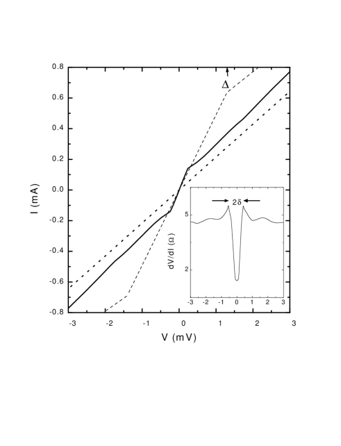
Figure 1 shows the I-V characteristics of a typical NIS sample measured by dc. These are compared with the I-V curve expected for an “ideal” junction namely, one having a unity Andreev coefficient. In the latter case for and for . For is characterized by a constant “excess-current” [1]. S and N subscripts are used here to designate measurables in the superconducting and normal state respectively. By comparison, the experimental curve shows for V=0.25 mV and has smaller excess-current at higher bias than the “ideal”.
The ratio, increases sharply just below the transition temperature of the Pb electrode, and it saturates at low temperatures as illustrated in figure 2. and were taken from the respective dV/dI plots at zero-bias, always making sure that the excitation current is small enough. The plots in the range 20 mV showed only weak structure (few percents in magnitude) that was L dependent. For L180 Å (L Å) a shallow dip (peak) centered at zero-bias was observed. In the intermediate regime (i.e., 180 Å Å), two shallow dips symmetrical with respect to V=0 were often observed with slightly different depths. This non-trivial behavior resembles that expected of resonant tunneling through two-level systems discussed by Galperin[4] and by Zawadowski[5] , and could be a relevant for the anomalies we observe.

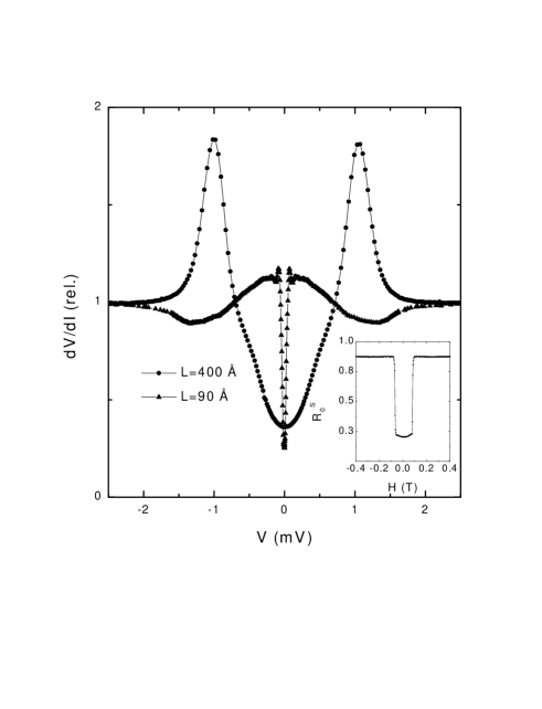
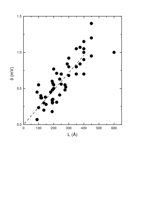
The samples studied in this paper had in the range 0.8-5 at 4K. Between room temperature and 100 K increased by up to one order of magnitude, depending on L, and below 10-20 K was temperature independent in all cases. This behavior is consistent with transport through a thin Anderson insulator (i.e., the indium-oxide layer) [6]. For T K, the of Pb, was obtained by applying a magnetic field H parallel to the sample plane to quench superconductivity (typically, 0.15 T). At higher fields, up to 3 T, was essentially unaffected by H. Within our experimental error this was identical with the zero-bias R measured just above . There is therefore no reason to believe that the large value of reported here is due to overestimating the value of . The majority of our samples (more than 80 samples altogether) had values between 2 and 4. Three samples had of about 5 and five samples had . No correlation was found between and or with the thickness of the Anderson insulator L. In fact, in a series of 3 samples prepared at the same deposition run, and where L was 200 Å, 400 Å, and 600 Å, was essentially the same for all three. On the other hand, there seems to be an intriguing correlation between L and the range of voltages, , over which the anomalous excess conductance is observed. It turns out that the smaller L is the narrower is this range, a trend that becomes quite apparent for samples with L Å. Figure 3 compares the dynamic resistance curves vs. bias voltage for a small L sample with a larger L sample clearly illustrating this point. A convenient measure of is the position of the peak in the dV/dI vs. V plot (c.f., inset to figure 1). The dependence of on L is shown in figure 4. Although there is a considerable scatter in the data the overall trend is clear. No such correlation could be identified between and . In particular, samples with identical L but with quite different junction areas (and therefore different ) exhibit similar .
Qualitatively, the zero-bias anomalies we observe have the features expected of NS contacts in which Andreev processes are dominant [1]. In particular, the correlation of the phenomenon with the appearance of superconductivity in the Pb electrode (c.f., figures 2 and 3) is suggestive of some sort of a proximity-effect. However, we are not able to account for the larger-than-two value of / or for the dependence of on L by any of the current models for NS contacts. While we cannot rule out structural imperfections, it is hard to see how they can explain the observed anomalies. For example, the I-V characteristics are incompatible with proximity-induced superconductivity in normal-metal filaments. The resistance of such a sample may go down below , but not by more than a factor of two, and it should gradually revert to its normal value (rather than saturate) at low temperatures. Also, in N/N’/S samples where N’ was a semi-continuous normal metal (a system which should closely resemble random array of filaments), the dependence of on L exhibited just the opposite trend than observed here [8]. Finally, the fact that goes to at the same H at which superconductivity is destroyed in the Pb electrode (figure 3) is inconsistent with transport through superconducting filaments [9].
While we cannot see how “technological” defects (that may or may not be there) can account for the anomalies we see, there is an inherent feature in the samples that must be reckoned with: The barriers in our samples are Anderson insulators, and that means that they include a significant density of localized states. This leads us to consider the possible role of the Anderson insulator in this problem. Andreev tunneling through such media received little theoretical attention to date so one can assess the relevance of this scenario only in general terms. It is established both theoretically [10] and experimentally [11] that coherent quantum mechanical effects can be observed in Anderson insulators. At helium temperatures the phase-coherent length in such systems is typically [11] few hundred Å which is comparable with L in our junctions, and therefore coherent tunneling through the medium is feasible. There are several indications that suggest that elastic tunneling processes take place in our samples. There are several indications that suggest that tunneling processes take place in our samples. In dV/dI plots of Pb//Pb devices with L Å we observed [3] a dip at V= and prominent modulations at V=4.5 mV and 8.5 mV, the phonon energies of lead[12]. These two features are clear evidence for Giaever tunneling. In the NIS devices this tunneling channel manifests itself as a dip in dV/dI at which can be clearly seen in samples with L Å (c.f., figure 3). Finally, all our samples, both NIS and SIS, show excess current at least up to voltages that are 5 times consistent with Andreev tunneling processes[1].
The correlation between and L may be also related to transport through localized states. Note that L is consistent with a characteristic electric field at which the process responsible for the large is broken or considerably weakened. As mentioned above, this feature is not observed in diffusive systems [8]. For Anderson insulators however, this result is natural because transport through localized states is very sensitive to electric fields [13]. A typical field associated with V= is F250 V/cm (estimated from the straight line in figure 4). Fields of these magnitudes are sufficient to appreciably reduce quantum-coherent effects associated with “forward-scattered” tunneling paths in Anderson insulators[14]. Andreev processes are even more sensitive to electric fields than single-particle processes because the electron and hole acquire different phases upon traversing it. This may become important in multiple scattering situations: As pointed out by van-Wees et al [15], the Andreev coefficient at the NS interface is enhanced by disorder due to a constructive interference between the electron and hole. This enhancement effect persists up to a critical voltage given by ( is the phase-breaking time of the disordered region at which the particle is “trapped” near the interface). For NS contacts this should lead to a zero-bias anomaly with voltage-width that decreases with L.
The situation in the NIS case, however, is different than that of the NS system in an essential way. To see that, consider a semi-infinite S and N layers separated by a layer of an Anderson insulator I of extent L along the Z-axis such that the SI interface is at Z=0 and the NI interface at Z=L. The electronic states in I are localized on scale much smaller than L. This introduces a natural hierarchy in the problem. States with Z0 are strongly coupled to S because on such scales there is no distinction between an Anderson insulator and a (dirty) normal metal. The conditions for the van-Wees et al mechanism are obeyed for this thin layer and therefore pairing-amplitude will be induced in it [16]. On the other hand, the states in N (that are responsible for the measured tunneling transport) have an exponentially small coupling to the superconductor because L. But this exponential coupling also makes the NS tunneling sensitive to modifications in the nature of the intermediate states in I, including those in . Now, the modification in the interface layer (and its effect on the I-V characteristics) is cut-off when the voltage drop across it exceeds . In other words we associate with the voltage across L that imposes a field . This immediately leads to the dependence L. To check on the plausibility of this approach note that using =10 Å as a typical value for the localization length in our samples [3], and =250 V/cm gives =/(e2 seconds which is a reasonable value for the inelastic time at these temperatures and fields [17].
Following van-Wees et al [15], it may be argued that applying a magnetic field should destroy the interference and thus weaken the zero-bias anomaly. But, the smallness of makes this field larger than that necessary to quench superconductivity in the Pb electrode. An ac field of frequency comparable to may be a more effective de-phasing agent in this case. We have indeed observed a dramatic reduction of ( in samples exposed to a 20 GHz microwave source. This reduction in the zero-bias conductance was much too big to be explained by the barely measurable Joule-heating of the sample due to the microwave field [18]. Full details of the microwave experiments will be given elsewhere [19].
This heuristic picture offers then a plausible way to understand the origin of the dependence of on L. The key question that remains to be answered is whether it can also account for the observation of /. This must await a detailed theoretical treatment of these issues. In particular the nature of the proximity-effect in Anderson insulators needs to be better understood. We hope that the present results will motivate such studies. We gratefully acknowledge useful discussions with M. Pollak. This research was supported by a grant administered by the Israel Science Foundation.
REFERENCES
- [1] G. E. Blonder, M. Tinkham and T.M. Klapwijk, Phys. Rev.B25, 4515 (1982).
- [2] A. Frydman and Z. Ovadyahu, Europhys. Letters, 33, 217 (1996).
- [3] A. Frydman and Z. Ovadyahu, Phys. Rev. B55, 9047 (1997).
- [4] Yu. M. Galperin et al, Phys. Rev, B49, 13728 (1994).
- [5] Zawadowski A., 1983 Phys. Rev. B28 1564. Zawadowski A, Phys. Rev. Letters, 45, 211 1980. See also, Ralp D. C. and Buhrman R. A., 1992 Phys. Rev. Letters, 69, 2118 and R.J.P. Keijsers et al, Phys. Rev. Lett. 77, 341 (1996).
- [6] M Pollak and J.J. Hauser, Phys. Rev. Lett. 31, 1304 (1973); M.E. Raikh and I. M. Ruzin, Sov. Phys. JETP 65, 1273 (1987).
- [7] P. Charlat, H. Courtois, Ph. Gandit, D. Mailly, A.F. Volkov and B. Pannetier, Phys. Rev. Lett. 77, 4950 (1996).
- [8] A. Frydman and R.C. Dynes, to be published.
- [9] A superconducting filament, whether extending across all or part of the junction width ought to have a much larger than that of the thick Pb electrode.
- [10] V.I. Neguyen, B.Z. Spivak and B. I. Shklovskii, JETP Lett. 60, 1566 (1988).
- [11] E. I. Lalko, A. 0. Orlov, A. K. Savchenko, E. A. Il’ichev, and E. A. Poltoratskii, Sov. Phys. JETP 66, 1258 (1987) [Zh. Eksp. Theor. Fiz., bf93, 2204 (1987)]; Z. Ovadyahu, Phys. Rev. B33, 6552 (1986).
- [12] A. Vaknin and Z. Ovadyhau, Phys. Stat. Sol., 205, 413 (1998).
- [13] B.I. Shklovskii, Fiz. Tekh. Poluprovodn. 10, 1440 (1976); M. Pollak and I. Riess, J. Phys. C: Solid State Phys. 9, 2339 (1979).
- [14] O. Faran and Z. Ovadyahu, Phys. Rev. B38, 5457 (1988); Z. Ovadyahu, in ”Hopping and Related Phenomena”, edited by H. Fritzsch and M. Pollak, Wold Scientific Publishing Company, (1990); Tremblay et al (ibid).
- [15] B.J. van Wees, P. de Vries, P. Magnee and T. M. Klapwijk, Phys. Rev. Lett. 69, 510 (1992); C.W.J. Beenakkar, Phys. Rev. B48, 2812 (1992).
- [16] Such an interference effect amounts to superconductivity being induced into a layer of extent of the Anderson Insulator. See also Yukio Tanaka and H. Fukuyama, in Coherence in high Temperature superconductors, eds., Deutscher and Revcolevschi, pp. 393-413, World Scientific (1996).
- [17] At T4 K and F100 V/cm the hopping length (and thus ) is controlled by F rather than by T (see references 14)
- [18] The shift in the sample temperature can be accurately measured by the position of the ‘above-gap’ structure which scales with (T), see reference 12 for details.
- [19] A. Vaknin and Z. Ovadyahu, to be published.