ATOMIC-SCALE MODELING OF THE DEFORMATION OF NANOCRYSTALLINE METALS
J. SCHIØTZ1,2,∗, T. VEGGE1,2, K. W. JACOBSEN1
1Center for Atomic-scale Materials Physics and Department of
Physics, Technical University of Denmark, DK-2800 Lyngby, Denmark
2Materials Research Department, Risø National Laboratory,
DK-4000 Roskilde, Denmark.
∗Email: schiotz@fysik.dtu.dk
abstract
Nanocrystalline metals, i.e. metals with grain sizes from 5 to 50 nm, display technologically interesting properties, such as dramatically increased hardness, increasing with decreasing grain size. Due to the small grain size, direct atomic-scale simulations of plastic deformation of these materials are possible, as such a polycrystalline system can be modeled with the computational resources available today.
We present molecular dynamics simulations of nanocrystalline copper with grain sizes up to 13 nm. Two different deformation mechanisms are active, one is deformation through the motion of dislocations, the other is sliding in the grain boundaries. At the grain sizes studied here the latter dominates, leading to a softening as the grain size is reduced. This implies that there is an “optimal” grain size, where the hardness is maximal.
Since the grain boundaries participate actively in the deformation, it is interesting to study the effects of introducing impurity atoms in the grain boundaries. We study how silver atoms in the grain boundaries influence the mechanical properties of nanocrystalline copper.
Introduction
In recent years, advanced production techniques have made it possible to create metals, alloys and ceramics with grain sizes down to 5 nm. For metals, this represents a reduction of the grain size by approximately four orders of magnitude compared to most conventionally produced metals. As can be expected, such a dramatic change in the microstructure leads to significant changes in the mechanical properties of the metals. For example, the hardness of typical nanocrystalline metals is far higher than what is seen in their coarse-grained counterparts [1, 2, and references therein].
Nanocrystalline metals are an attractive group of metals to model, as the small grain size provides a “cut-off” of the typical length scales, where structures appear during deformation. In coarse-grained materials structures appear on vastly different length scales, making it very difficult to model the properties of these materials. The models must include processes that occur on length scales from the sub-nanometer scale of the atomic processes in dislocation cores, to the micro- or even millimeter scale of grain and subgrain structures [3, 4]. Atomic-scale simulations of systems of these sizes are beyond the reach of even the most powerful of todays supercomputers. One is thus forced to split the system into sub-problems at different length-scales, and only treat sub-problems at the atomic scale with atomistic models. On coarser length scales other modeling paradigms must be used, such as Dislocation Dynamics and continuum plasticity calculations.
Dividing the problem into sub-problems at different length scales often results in a better understanding of the problem, as it draws attention to the structures which are relevant at a given length scale (for example, when studying the formation of dislocation structures it is clearly more relevant to focus on dislocations as the fundamental concept rather than on individual atoms). On the other hand, one becomes dependent on this understanding, when creating the coarse-grained models, as many assumptions about the relevant phenomena at different length-scales will by necessity be built into the multi-scale model. The low grain size of nanocrystalline metals “compresses” this range of length scales to a range, where the whole deformation problem can be modeled at the atomic scale, as many grains in the polycrystalline material can be handled in an atomic-scale simulation. This makes it possible to perform unbiased simulations of the deformation process, where no a priori assumptions are made about the deformation mechanisms.
In recent papers, we have presented simulations of the plastic deformation of nanocrystalline Cu and Pd [5, 6, 7]. Other authors have presented simulations of the structure and elastic properties of nanocrystalline metals and semiconductors [8, 9, 10, 11, 12], and of the plastic deformation of Ni under constant stress loading [13, 14]. In this paper we review our simulations of the deformation mechanisms in nanocrystalline metals, and present simulations of the effects of impurities in the grain boundaries.
Simulations of pure metals
Simulation setup

We have attempted to generate three-dimensional systems with a microstructure similar to that observed experimentally in samples generated by inert gas condensation (IGC). The grains appear to be randomly oriented, approximately equiaxed, and dislocation free. The grain size distribution is close to log-normal [1, 15, and references therein]. We try to create systems that match this description.
The grains are produced using a three-dimensional Voronoi tesselation: random grain centers are chosen, and space is divided into regions in such a way that each region consists of the points in space closer to a given grain center than to any other grain center. Each region is then filled with a randomly oriented fcc lattice. An example of a two-dimensional Voronoi tessellation is shown in Figure 1.
The generated samples are annealed for 50 ps at 300 K to relax the grain boundary structure. We found that the annealing time and temperature are uncritical, but that the properties of the system are different if no annealing is done.
The interactions between the atoms are modeled using the Effective Medium Theory (EMT) [16, 17]. EMT is a many-body potential providing a realistic description of the metallic bonding, in particular in face-centered cubic (fcc) metals and alloys of fcc metals. Computationally, EMT is not much more demanding than pair potentials, but provide a significantly more realistic description of the metallic bonding.
The systems were deformed using a molecular dynamics (MD) procedure. A conventional MD simulation was performed, but at each timestep the atomic coordinates in the pulling direction (the coordinates) were rescaled in order to deform the system gradually. At the same time, the box dimensions in the transverse directions are allowed to shrink to keep the transversal components of the stress ( and ) close to zero [7]. The change in system dimensions is slow at the timescale of the simulation, the relative elongation is each timestep. With a timestep of 5 fs, this nevertheless results in a very high strain rate (). The results presented here are not very sensitive to the strain rate, although some dependence is seen (typical stresses increase by 20% when the strain rate is changed from to ) [7].
Results
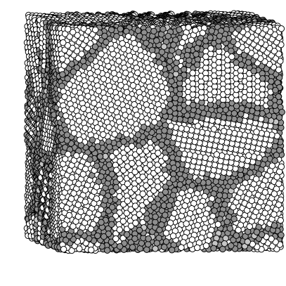
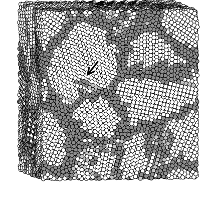
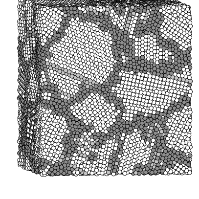

Figure 2 shows the deformation of a typical sample with an average grain size of 5.21 nm. The atoms have been color coded according to the local crystal structure [18, 19]. White atoms are in local fcc order, and thus situated inside the grains. Light grey atoms are in local hexagonal close-packed (hcp) order, these atoms are at stacking faults. Atoms in all other local environments are colored dark grey. These are typically atoms at grain boundaries and in dislocation cores.
Some dislocation activity is seen in the system, as witnessed by the generation of stacking faults. The dislocation activity is not sufficient to account for the observed plastic deformation. A detailed analysis of the deformation shows that the main deformation mode is sliding in the grain boundaries [5, 7].
As the volume fraction of atoms in the grain boundary increases with decreasing grain size, one would expect that increasing the grain size increases the strength of the material as long as the grain boundaries remain the carriers of the deformation. This is indeed what we see in the simulations. Figure 3 shows the stress-strain curves obtained from simulations of systems with various average grain sizes. A “reverse Hall-Petch effect”, i.e. a softening of the material with decreasing grain size, is observed.

Discussion
The simulations of the deformation of nanocrystalline metals show a reverse Hall-Petch effect in Cu and Pd for the grain sizes studied. This softening of the material, when the grain size is reduced is caused by plastic deformation in the grain boundaries. There appears to be two different deformation mechanisms active at different grain sizes. In metals with the very small grain sizes studied here, the dominating deformation mechanism is sliding in the grain boundaries through a large number of essentially uncorrelated events, where a few atoms move with respect to each other at each event [5].
At much coarser grain sizes, dislocations are known to be the dominating carriers of deformation. In that regime, a hardening of the material is seen, when the grain size is reduced, as the grain boundaries act as barriers to the dislocation motion. Experimentally, this behavior is seen to continue far down into the nanocrystalline range.
As the grain size is reduced, dislocation-mediated deformation becomes more and more difficult. On the other hand, the volume fraction of the grain boundaries increases, favoring a deformation mechanism where the grain boundaries carry the deformation. Furthermore, as the grain size is approaching the grain boundary thickness, it becomes geometrically easier for slip to occur on more than one grain boundary, without large stress concentrations where the grain boundaries meet [20].

The emerging picture is one where two deformation mechanisms compete. One is active at very small grain sizes, another at larger grain sizes. This leads to a maximum in the yield stress and hardness of nanocrystalline metals at intermediate grain sizes, see Figure 4.
There have been many reports in the literature of a “reverse Hall-Petch effect” at sufficiently small grain sizes. However, the hardness measurements are very sensitive to sample defects, and in particular to sample porosity [21, 22, 23]. In high-quality Cu samples, the Hall-Petch effect is seen to continue at least down to grain sizes around 15 nm [21].
There does not appear to be any unequivocal experimental evidence for a reverse Hall-Petch relationship in porosity free nanocrystalline metals. There are, however, indications of a break-down of the ordinary Hall-Petch relation at grain sizes below 15 nm in high quality copper samples produced by inert gas condensation [21]. The ordinary Hall-Petch effect appears to cease, although a reverse Hall-Petch relation is not seen. It is still difficult to make direct comparisons between simulations and experiment, as there is little overlap in grain size. As the experimental techniques improve, there is hope that more experimental data will be gathered on high-quality samples with grain sizes below 10–15 nm. It should then become clear if the Hall-Petch effect does indeed break down at these grain sizes. At the same time, computer simulations of larger systems might lead to observations of the cross-over region between the reverse and the ordinary Hall-Petch effect. That cross-over region is beyond the reach of the largest simulations presented here. The grain boundaries remain the main carriers of the deformation even when the grain size is increased to 13.2 nm, but be do observe a slight increase in dislocation activity as the grain size is increased.
The effects of alloying
As the main deformation mechanism is sliding in the grain boundaries, it could be expected that altering the structure and composition of the grain boundaries might have an effect on the properties of the material. One such modification is the addition of impurity atoms in the grain boundaries.
We have chosen to study the effects of silver impurities. A reason for choosing silver was that silver and copper are immiscible, low concentrations of silver impurities in nanocrystalline copper can therefore be expected to segregate to the grain boundaries. We have not studied the segregation process itself, as it is beyond the scope of this study. Segregation is a slow, diffusional process that cannot be studied directly with MD simulations due to the timescales involved. Other approaches (such as Monte Carlo or Kinetic Monte Carlo simulations) may be more appropriate.
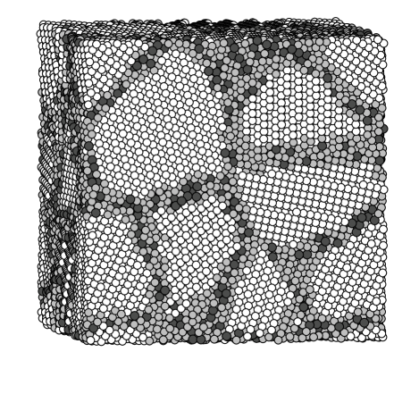
Instead of simulating the segregation process, we have generated systems that model nanocrystalline copper after such a segregation has occurred. It is done by replacing 25% of the atoms in the grain boundaries with silver atoms, see Figure 5. The system is then annealed and deformed in the same way as the pure systems.


Figure 6 shows how the stress-strain curves have changed, when silver is introduced in the grain boundaries. The general trend seems to be a slight softening of the material, although the effect is very weak and not seen in all systems. Figure 7 shows the flow stress levels for the different simulations, i.e. the stress level at the horizontal part of the stress-strain curve (for simplicity the flow stress was defined as the average stress for ). We again see the tendency for the silver-containing systems to be softer.
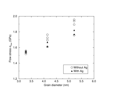
In the simulations of impurities in the grain boundaries, the mechanical behavior is close to what is seen in the pure systems.
As the major part of the deformation happens in the grain boundaries, one could expect that adding impurities in the grain boundaries could have a relatively large effect on the mechanical properties. The simulations presented here show that this is not the case, when silver is used as impurities in copper. We see a tendency towards a weakening of the material, but the effect is barely detectable.
The atomic bonding in copper and silver are of a similar nature, and the size of the atoms are not very different. This may account for the absence of a stronger effect of alloying in the grain boundaries.
Conclusion
Atomic-scale simulations have been used to study the deformation mechanisms in nanocrystalline copper with and without impurities in the grain boundaries. In both cases, we find that the main deformation mode is sliding in the grain boundaries through a large number of apparently uncorrelated events, each involving only a few atoms. Some dislocation activity is seen in the grains, the dislocations are probably necessary to allow the grains to deform a little, as they glide past each other.
We observe a reverse Hall-Petch effect, i.e. a hardening of the material as the grain size is increased: as the amount of grain boundary atoms is decreased, the deformation becomes harder. At the same time the dislocation activity is seen to increase a little with grain size. This effect is seen in the entire range of grain sizes that we have studied (3 to 13 nm), but at some point we expect that dislocation motion will begin to dominate the behavior of the system. When that happens, the yield strength should begin to decrease with increasing grain size.
Adding silver to the grain boundaries has only a weak effect on the properties of the material. The strength of the material is seen to decrease marginally, when the silver is introduced. We expect that other elements, which chemically behave in a way that is more different from copper will have a larger effect, but such simulations remain to be made.
Acknowledgments
This work was financed by The Danish Technical Research Council through Grant No. 9601119. Parallel computer time was financed by the Danish Research Councils through Grant No. 9501775. Center for Atomic-scale Materials Physics is sponsored by the Danish National Research Council.
REFERENCES
- [1] R. W. Siegel and G. E. Fougere, in Nanophase Materials: Synthesis — Properties — Applications, edited by G. C. Hadjipanayis and R. W. Siegel, vol. 260 of NATO-ASI Series E: Applied Sciences, p. 233 (Kluwer, Dordrecht, 1994).
- [2] D. G. Morris and M. A. Morris, Mater. Sci. Forum, 235-238, p. 861 (1997).
- [3] J. V. Carstensen, T. Leffers, T. Lorentzen, O. B. Pedersen, B. F. Sørensen, and G. Winther, eds., Modelling of Structure and Mechanics of Materials from Microscale to Product, Proceedings of the 19th Risø International Symposium on Materials Science, Risø National Laboratory, Roskilde (1998).
- [4] A. E. Carlsson and R. Thomson, Solid State Physics, 51, p. 233 (1998).
- [5] J. Schiøtz, F. D. Di Tolla, and K. W. Jacobsen, Nature, 391, p. 561 (1998).
- [6] J. Schiøtz, T. Vegge, F. D. Di Tolla, and K. W. Jacobsen, in Carstensen et al. [3], p. 133.
- [7] J. Schiøtz, T. Vegge, F. D. Di Tolla, and K. W. Jacobsen, Atomic-scale simulations of nanocrystalline metals, (to be published).
- [8] D. Chen, Comput. Mater. Sci., 3, p. 327 (1995).
- [9] S. R. Phillpot, D. Wolf, and H. Gleiter, J. Appl. Phys., 78, p. 847 (1995).
- [10] S. R. Phillpot, D. Wolf, and H. Gleiter, Scripta Met. Mater., 33, p. 1245 (1995).
- [11] H. Zhu and R. S. Averback, Materials and Manufacturing Processes, 11, p. 905 (1996).
- [12] P. Keblinski, R. Phillpot, D. Wolf, and H. Gleiter, Acta Mater., 45, p. 987 (1997).
- [13] H. Van Swygenhoven and A. Caro, Appl. Phys. Lett., 71, p. 1652 (1997).
- [14] H. Van Swygenhoven and A. Caro, NanoStructured Materials, 9, p. 669 (1997).
- [15] R. W. Siegel, J. Phys. Chem. Solids, 55, p. 1097 (1994).
- [16] K. W. Jacobsen, J. K. Nørskov, and M. J. Puska, Phys. Rev. B, 35, p. 7423 (1987).
- [17] K. W. Jacobsen, P. Stoltze, and J. K. Nørskov, Surf. Sci., 366, p. 394 (1996).
- [18] H. Jónsson and H. C. Andersen, Phys. Rev. Lett., 60, p. 2295 (1988).
- [19] A. S. Clarke and H. Jónsson, Phys. Rev. E, 47, p. 3975 (1993).
- [20] H. Hahn and K. A. Padmanabhan, Phil. Mag. B, 76, p. 559 (1997).
- [21] P. G. Sanders, C. J. Youngdahl, and J. R. Weertman, Mater. Sci. Eng. A, 234-236, p. 77 (1997).
- [22] P. G. Sanders, J. A. Eastman, and J. R. Weertman, Acta mater., 46, p. 4195 (1998).
- [23] S. R. Agnew, B. R. Elliott, C. J. Youngdahl, K. J. Hemker, and J. R. Weertman, in Carstensen et al. [3], p. 1.