Negative Differential Resistance in the Scanning Tunneling Spectroscopy of Organic Molecules
Abstract
The conductance-voltage spectrum of molecular nanostructures measured by scanning tunneling spectroscopy (STS) is generally assumed to reflect the local density of states of the molecule. This excludes the possibility of observing negative differential resistance (NDR). We report here the observation of NDR in the scanning tunneling microscope (STM) current-voltage (I-V) characteristics of self-assembled monolayer (SAM) of 4-p-Terphenylthiol molecules on gold substrate measured using a platinum probe. We argue that the NDR arises from narrow structures in the local density of states at the tip apex atom and show that depending on the electrostatic potential profile across the system, NDR could be observed in one or both bias directions.
pacs:
PACS number: 73.61.Ph, 61.16.ChElectron transport through molecular nanostructures has been widely studied in recent years, using either the scanning tunneling microscope or mechanically controllable break junctions[1, 2]. The conductance-voltage spectrum, , is commonly assumed to reflect the local density of states (LDOS) of the molecule[3]: , being the equilibrium Fermi energy. A more accurate description of the conductance-voltage spectrum, as shown in Ref.[1], is to take a weighted average of the density of states:
| (1) |
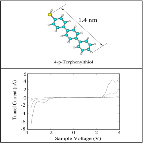
Here and are the electrochemical potentials in the two contacts and the factor describes the voltage division across the molecule: and . Based on this viewpoint, NDR, i.e., a negative slope in the I-V curve, cannot occur since the density of states is nonnegative. Experimentally, however, we often observe negative differential resistance for monolayer of long molecules self-assembled on gold substrate such as the one shown in Fig. 1.
A possible scenario that can lead to NDR at the atomic level was studied theoretically by Lang[4] and experimentally by Avouris and co-workers[5]. The essential argument is that if there is a weak link between two parts of the conducting system, each of which has relatively narrow features in the density of states in the energy range of interest, NDR is likely to occur. This is readily understood from the transfer Hamiltonian point of view[6], which relates current to the product of the density of states and on both sides of the weak link. As the bias is changed, current can decrease if two narrow structures in and move away from alignment. For the structure we studied (Fig. 2), the weak link is the STM tip-molecule junction. If the tip has a featureless density of states, as is implicitly assumed in the derivation of Eq. (1), we wouldn’t expect this scenario to apply. However, narrow features in the density of states can develop at the tip atoms in a realistic model of tip. This has been widely recognized in the STM study of surfaces[6] and is used to explain the NDR in STM I-V characteristics of boron-exposed silicon surface[5]. More recently, Yeyati et al. [7] have studied the electronic structure of a sharp gold tip in the context of conductance quantization in gold atomic-size contacts and shown that narrow resonant states can develop at the tip apex atom provided the tip geometry is sufficiently sharp.
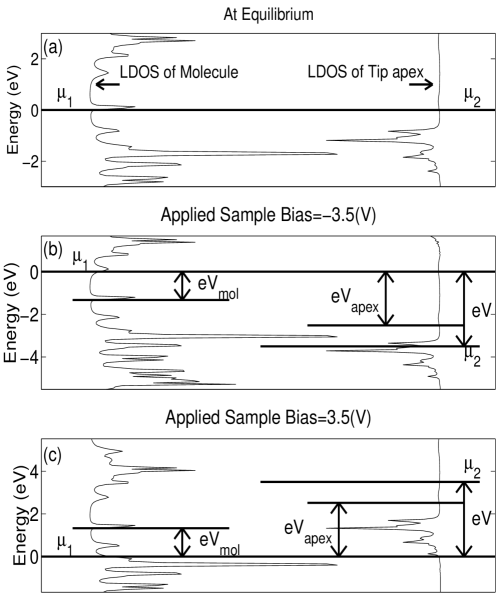
In this paper we explain the occurrence of NDR by taking into account the electronic structure of sharp platinum tip (used in our STM measurement [8]) as well as the electrostatic potential profile across the tip/molecule system. Using a tip model similar to Yeyati et al. [7], we find narrow structures in the LDOS of tip apex atom below the equilibrium Fermi energy (Fig. 3(a)). Since the LDOS of molecule also exhibits sharp structures, we expect NDR to occur under applied bias. However, since the narrow structures of LDOS at tip apex atom are below , NDR will occur only at positive sample bias if the electrostatic potential at the tip apex atom is the same as that of the tip support. But NDR can occur in both bias directions if a significant amount of the voltage is dropped between the tip apex atom and the tip support. We argue that for very sharp tip geometry, this is likely to be true when the tip is close to the molecule. Since the tip is composed of a small cluster of platinum atoms, the screening length in this region can be much larger than that in the bulk and also larger than the cluster size, making it possible to maintain an electrostatic potential drop between the tip apex and the tip support under applied bias. Experimentally, we observe NDR in both bias directions when the tip is very close to the molecule, in agreement with the theory.
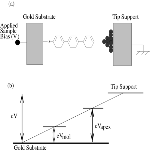
Our model is illustrated in Fig. 2(a). The self-assembled monolayer (SAM) of 4-p-Terphenylthiol molecules are synthesized using standard procedure. I-V data presented here (Fig. 1) represents the average of 25-50 consecutive I(V) sweeps taken at a fixed position on the sample[9]. The SAMs attach strongly to the gold surface through the sulfur end atom forming a strong chemical bond with good orbital overlap[10]. The STM tip usually couples weakly to the molecule, corresponding to the physisorption situation. As in our previous studies[1], we’ll use the Extended Hückel Theory (EHT) to describe the whole molecule-STM system (for a recent justification of using EHT in STM study of metal surfaces, see Ref. [11]), taking into account the orbitals of platinum and gold.
Similar to Yeyati et al. [7], we model the tip geometry as a small cluster of Pt atoms stacked on the surface of semi-infinite support[12], originating from a monatomic apex, adding 3 nearest neighbor atoms to the 2nd layer and 7 nearest neighbor atoms to the 3rd layer (we also include 14 nearest neighbor atoms on the surface of the tip support and 6 atoms on the gold substrate surface in the calculation of I-V characteristics). The on-site energies for the orbitals of the 3 layers of tip atoms are modified self-consistently by adjusting the occupation number of each orbital to that of the neutral atom until local charge neutrality is achieved on each atomic site[7, 11, 18].
We calculate current using[13]:
| (2) | |||||
| (3) |
where is the Fermi distribution and , are the electrochemical potential of the gold substrate and tip support respectively, [14]. The transmission can be calculated using the scattering theory of transport, as we shall describe shortly, but we can get more insight if we use the transfer Hamiltonian formalism[6] to relate the transmission to the local density of states on either side of the STM tip-molecule junction:
| (4) |
where is the coupling matrix element and and are the electrostatic potentials of the molecule and the tip apex atom respectively.
The LDOS of both the molecule and the tip apex atom show narrow features (Fig. 3(a)), which are calculated from the Green’s function of molecule-tip system using[15]:
| (5) |
where is defined by , and is the overlap matrix. The narrow structures of LDOS at tip apex can be understood qualitatively from the fact that platinum is third row transition metal, whose LDOS around the equilibrium Fermi energy is mostly due to the contribution of the 5d orbitals, located slightly below . For the given sharp tip geometry, the coupling of the tip apex atom to its local environment is much weaker comparing to that in the bulk, so the levels remain fairly sharp.
What is the electrostatic potential profile? Applying an external bias changes the relative electrochemical potential of the gold substrate and tip support, which are taken as infinite electron reservoirs. The electrostatic potential is determined self-consistently from the Poisson equation . We only need to calculate the change in electrostatic potential (which in turn modifies the molecular Hamiltonian) since its equilibrium value has been included in the equilibrium Hamiltonian. The electrostatic potential change in each electrode follows that of the electrochemical potential which provides boundary condition to the Poisson equation. The important point is that we take the 3 layers of tip atoms and the molecule on an equal footing, viewing the whole molecule-tip system as an “extended molecule” sandwiched between the two electrodes. In the region near the tip apex, both the electrochemical and the electrostatic potential can be different from those inside the tip support and from each other[16].
As a first approximation, if we neglect any charge buildup within the molecule-tip system, and assume that the gold substrate and tip support act as two infinite parallel plates of a capacitor, then the electrostatic potential varies linearly, as shown in Fig. 2(b). For simplicity, we assume that the molecular energy levels simply float up by an amount around the average electrostatic potential change, that is, we neglect any Stark shift of the energy levels due to the electric field inside the molecule[17]. The origin of NDR can be best understood by examining how the LDOS structures of the molecule and the tip apex atom sweep past each other under applied bias (Fig. 3). NDR will occur for both bias directions if we assume a significant voltage drop between the tip apex and the tip support, i.e., , as evident from Fig. 3.
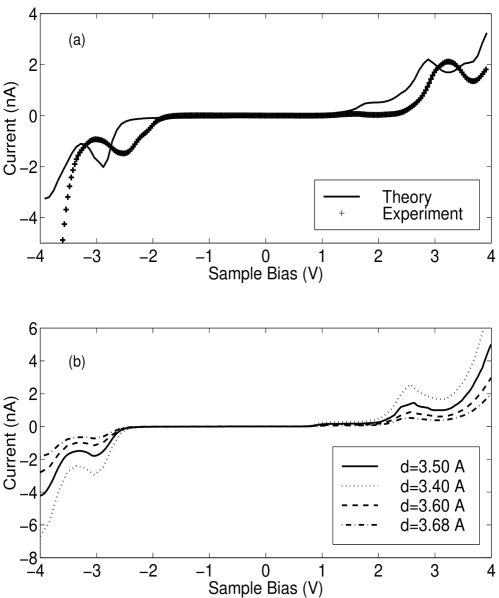
It can be seen from Fig. 4(a) that this approach predicts the I-V characteristics quite well with four fitting parameters, namely the tip-molecule distance, the equilibrium Fermi energy , the constant coupling matrix element and the electrostatic potential change of the molecule. We also calculated the transmission function using the equation (see page in Ref. [13]):
| (6) |
which goes beyond the transfer Hamiltonian formalism and takes arbitrary sample/electrode coupling into account. Also, a better approximation to the electrostatic potential should take charging effects within the molecule into account. In tight-binding theory, this gives , where is the average elctrostatic potential change of the molecule without charge buildup and is the excess number of electrons in the molecule induced by the applied bias. Since the molecule is strongly coupled to the gold substrate, we can assume that it is in equilibrium with the gold substrate and get by solving the following self-consistent equation:
| (7) | |||||
| (8) |
The charging energy U can be estimated from the energy gap in molecular optical spectra, electron affinity and ionization potential of the molecule: , where is the optical gap and is the image potential due to the substrate [18]( is the distance from the center-of-mass of molecule to the substrate). Since eV, eV, and Å, is eV. We have used eV in our calculation. The resulting electrostatic potential change is included in the calculation of the Green’s function and transmission probabilities using Eq. (6). Results of such calculation show similar qualitative features to that obtained from the simple transfer Hamiltonian argument (Fig. 4(b)).
In conclusion, we have presented a simple explanation of the NDR in STM I-V characteristics of self-assembled monolayer of 4-p-Terphenylthiol molecules in terms of the electronic structure of sharp platinum tip. The major approximation in our theory is the use of the Extended Hückel theory and a simplified treatment of electrostatic potential variation. A central factor in understanding the NDR is the narrow structures in the LDOS at the tip apex which has been noted by other authors in different contexts. However, this alone is not enough to explain the occurrence of NDR in both bias directions. NDR for negative sample bias can be understood only if we allow for an electrostatic potential drop between the tip apex and the tip support. This is possible for very sharp tip geometries, where screening length is large. But if the tip is relatively flat, the potential drop between the tip apex atom and the tip support will be reduced. Indeed, experimentally we do observe NDR only in positive sample bias direction for some of our tips. However, even with these tips, we observe NDR in both bias directions when we move the tips closer to the molecule, indicating a significant increase in the potential drop between the tip apex and the tip support. It’s not clear to us why the potential drop should increase significantly, since the distance range by which the tips move is relatively narrow. Perhaps a more complete theory is needed that involves self-consistent evaluation of the electronic structure for the entire electrode/sample system, such as described by Lang[19]. Our main purpose here, is then to show that the electrostatic potential profiles play a crucial role in determining the shape of I-V characteristics of molecular nanostructures— a role that has not been adequately recognized.
This work was partially funded by the National Science Foundation under Grant No. 9708107-DMR. One of us (R.R.) would like to thank Norton Lang for a stimulating discussion during the very early stages of this work.
REFERENCES
- [1] S. Datta et al. , Phys. Rev. Lett. 79, 2530 (1997).
- [2] M.A. Reed et al., Science 278, 252 (1997).
- [3] J. Tersoff and D.R. Hamann, Phys. Rev. B 31, 805 (1985); N.D. Lang, Phys. Rev. B 34, 5947 (1986).
- [4] N.D. Lang, Phys. Rev. B 55, 9364 (1997).
- [5] I. -W. Lyo and Ph. Avouris, Science 245, 1369 (1989).
- [6] Scanning Tunneling Microscopy III, edited by R. Wiesendanger and H.-J. Güntherodt (Springer-Verlag, Berlin, 1993).
- [7] A.L. Yeyati, A. Martín-Rodero and F. Flores, Phys. Rev. B 56, 10369 (1997).
- [8] Technically, Pt/Ir tips with composition 80:20 were used (Ir atoms have little effect on the tip electronic structure).
- [9] Seunghun Hong, Ph.D thesis, Department of Physics, Purdue University.
- [10] Y. Xia and G.M. Whiteside, Adv. Mater. 7, 471 (1995).
- [11] J. Cerdá et al. , Phys. Rev. B 56, 15885 (1997); J. Cerdá et al. , Phys. Rev. B 56, 15900 (1997).
- [12] V.T. Binh and J. Marien, Surf. Sci. 202, L539 (1988); T.N. Todorov and A.P. Sutton, Phys. Rev. Lett. 70, 2138 (1993).
- [13] S. Datta, Electron Transport in Mesoscopic Systems (Cambridge University Press, Cambridge, 1995).
- [14] Under zero bias, both and are equal to the equilibrium Fermi energy of the STM-molecule system which can be determined in principle using the relation (N is the number of electrons in the molecule, see Ref. 1). However, the resulting curve shows quick variation in the region around the neutral case, making it better to use as a fitting parameter in this region (experimentally the charge transferred between the contacts and the molecule at equilibrium is usually much less than one electron).
- [15] M.P. López Sancho, J.M. López Sancho and J. Rubio, J. Phys. C 18, 1803 (1985).
- [16] M.J. Mclennan, Y. Lee and S. Datta, Phys. Rev. B 43, 13846 (1991).
- [17] In general, the molecule will be polarized by an external electric field, whose polarization can be calculated using a self-consistent procedure such as density functional theory. This effect will reduce the electric field within the molecule and correspondingly, giving rise to a larger potential drop across the tip than that obtained from the assumption of linear potential variation.
- [18] M.C. Desjonquères and D. Spanjaard, Concepts in Surface Physics, 2nd Edition (Springer-Verlag, Berlin, 1996).
- [19] N.D. Lang, Phys. Rev. B 52, 5335 (1995); N.D. Lang and Ph. Avouris, Phys. Rev. Lett. 81, 3515 (1998).