Conductances in normal and normal-superconductor structures
Abstract
We study theoretically electronic transport through a normal metal – superconductor (NS) interface and show that more than one conductance may be defined, depending on the pair of chemical potentials whose difference one chooses to relate linearly to the current. We argue that the situation is analogous to that found for purely normal transport, where different conductance formulae can be invoked. We revisit the problem of the “right” conductance formula in a simple language, and analyze its extension to the case of mesoscopic superconductivity. The well-known result that the standard conductance of a NS interface becomes 2 (in units of ) in the transmissive limit, is viewed here in a different light. We show that it is not directly related to the presence of Andreev reflection, but rather to a particular choice of chemical potentials. This value of 2 is measurable because only one single-contact resistance is involved in a typical experimental setup, in contrast with the purely normal case, where two of them intervene. We introduce an alternative NS conductance that diverges in the transmissive limit due to the inability of Andreev reflection to generate a voltage drop. We illustrate numerically how different choices of chemical potential can yield widely differing I–V curves for a given NS interface.
pacs:
PACS numbers: 72.10.Bg, 74.50.+r, 74.80.Fp, 74.90.+nI Introduction
Since the early work by Landauer [1], the scattering picture has provided a useful framework for theoretical studies on electron transport in small structures. In the eighties, a debated question [2, 3] was whether the (zero temperature) conductance formula for a barrier in a one-dimensional wire is
| (1) |
or, rather,
| (2) |
where and is the probability that an electron is transmitted across the barrier, as indicated in Fig. 1a. The consensus emerged that Eq. (1) is relevant as a two-lead conductance formula, while Eq. (2) should better describe a four-lead conductance. Eqs. (1) and (2) were generalized to the multi-channel case by Büttiker et al. [4], and a multi-lead extension of Eq. (1) was derived by Büttiker [5, 6].
In this article, we wish to address the problem of the “right” conductance formula in the context of mesoscopic superconductivity. We will argue that, what is usually presented as the definition of conductance in a normal-superconductor (NS) interface, is just a particular (albeit rather natural) choice. We begin by reviewing the work of Ref. [4] in a slightly different language which will permit a convenient generalization to the NS case. For greater clarity, we focus on one-dimensional transport, neglecting the complication that, in reality, a stable superconductor requires higher dimensions.
We adopt the point of view that the two different conductance formulae (1) and (2) are equally valid for a given sample, the difference lying in the choice of chemical potentials to which the electric current is linearly related. Normal transport requires the existence of differences among the chemical potentials of several subsets of carriers. Hence it should come as no surprise that, if the same electric current can be related to more than one pair of chemical potentials, it is possible to formulate more than one definition of conductance. If one reviews a standard derivation of Eq. (1) (see for instance Refs. [5, 6]), one may note that the chemical potentials which are invoked are those which characterize the population of electrons in the incoming channels. In terms of these chemical potentials, the electric current can be calculated to be
| (3) |
where () is the chemical potential for electrons impinging on the sample from the left (right) lead, as schematically shown in Fig. 1a. One readily notes that the conductance formula (1) results from defining [7]
| (4) |
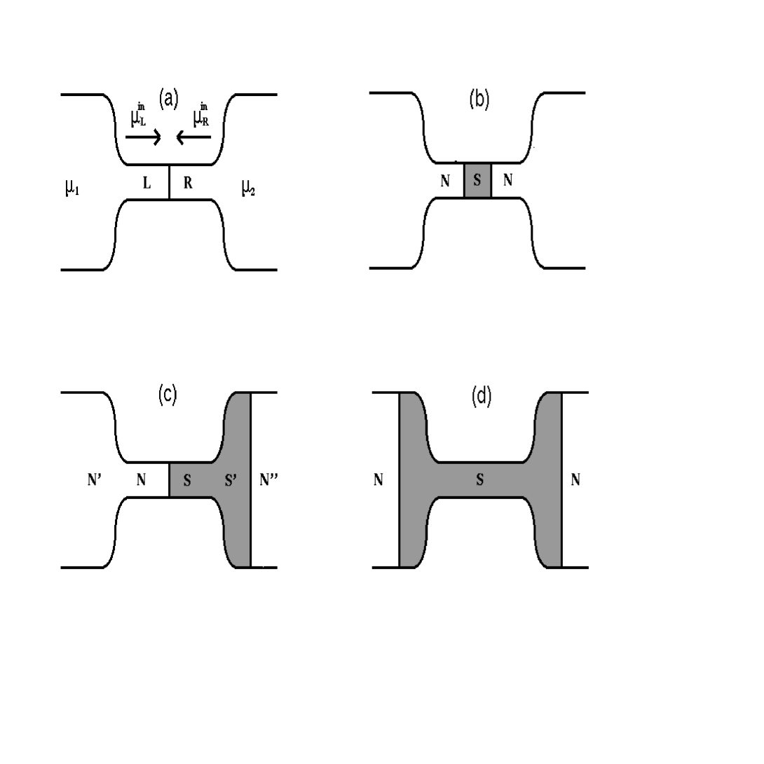
A standard assumption is that both leads are connected to broad reservoirs through ideal contacts lacking internal reflection, as depicted in Fig. 2a. This permits us to assert that all incident electrons come directly from the reservoirs, those in each lead possessing an internal thermal distribution which is identical to that of their original reservoir (which, by construction, can be assumed to be in equilibrium). In particular, we can write and , where and are the chemical potentials of the left and right reservoirs, respectively. This identification of the chemical potentials of the incoming electrons with those of the broad reservoirs where voltage is eventually measured, justifies the label “two-lead conductance” for Eq. (1).
Unlike the incident electrons, one may expect the outgoing electrons in a given lead to incorporate properties from both reservoirs. Assuming that the population of electrons emerging from the sample can be described appropriately by chemical potentials and (see Fig. 1a), one expects the following relations to hold:
| (5) | |||||
| (6) |
Eq. (5) provides an intuitive ansatz for the outgoing chemical potentials in terms of the incoming chemical potentials which explicitly invokes the scattering properties of the sample. In Appendix A, we provide a rigorous derivation of Eq. (5) and explicitly prove its equivalence to related equations derived in Ref. [4].
One may define an average chemical potential for each lead,
| (7) |
which is directly associated to the total electron density. It is easy to prove that
| (8) |
which permits to rewrite (3) as
| (9) |
This result indicates that in Eq. (2) is obtained from relating the electric current to differences between the average chemical potentials associated to the total electron density in each lead, i.e., we can define
| (10) |
and obtain (2). Since is the voltage one would measure by attaching noninvasive capacitive (or, in general, weakly coupled) probes to both sides of the sample [3, 6, 8, 9], hence the label “four-probe conductance” some times employed for Eq. (2).
Within this simple approach to the problem, the choice of conductance formula reduces to the selection of two particular subsets of electrons whose chemical potential difference is linearly related to the current. There is no strict need to explicitly invoke concepts such as reservoirs or capacitive probes. The whole conductance problem can be formulated in terms of intrinsic scattering concepts. A different question is what is the conductance that one actually measures in a particular experimental setup [3] or that is relevant in a specific theoretical context.
II Conductances in a normal-superconductor interface
Now we wish to extend this discussion of the conductance problem to the case of a normal metal – superconductor interface. A scattering approach to electron transport through NS interfaces was already advocated by Demers and Griffin [10], and by Blonder et al. [11], long before such a viewpoint became popular in theoretical studies of normal transport. The systematic extension of ideas on normal mesoscopic transport to systems involving both normal and superconducting elements was initiated by Lambert [12], Beenakker [13], and Takane and Ebisawa [14, 15]. However, neither in these nor in other ensuing works has an explicit discussion been presented of the conductance problem in NS interfaces [16, 17, 18]. Rather, the view has implicitly been adopted that there is only one NS conductance, which is the natural generalization of Eq. (1). For the sake of simplicity, we focus on the low-voltage regime in which normal and Andreev reflection are the only outgoing scattering channels for quasiparticles impinging from the normal lead N on the superconductor S, in the structures shown schematically in Figs. 1b and 2c. Quasiparticle number conservation requires , where () is the probability for Andreev (normal) reflection from the NS interface. A microscopic calculation shows that
| (11) |
where is the chemical potential for incoming quasiparticles on the N side. At sufficiently low temperatures and voltages, there are no quasiparticles in S, which is thus described by a single chemical potential . Eq. (11) yields the famous NS conductance formula [11, 12, 13, 14]
| (12) |
A wave function matching calculation shows that, at low energies [11, 13],
| (13) |
where is the probability for electron transmission in the normal state of the interface. Eq. (13) tells us that, in the tranmissive () limit, Andreev reflection becomes the dominant process (). This limit will be discussed in depth later.
Below we show that a second NS conductance other than (12) can be introduced which is reminiscent of Eqs. (2) and (10) for the normal case. We begin by presenting an ansatz for the outgoing chemical potential that adapts (5) to a NS context. Since there are no quasiparticles on the S side, we only have to deal with one incoming and one outgoing channel, both on the N side (here we view electrons and holes indistinctly, as terms which describe the occupation of a unique set of electron states). In Appendix A, we show that the single relation that expresses in terms of must read (see Fig. 1b)
| (14) |
The presence of quasiparticles at nonzero temperatures or high enough voltages would of course complicate the picture slightly. The negative sign accompanying the Andreev reflection probability in the l.h.s. of Eq. (14) reflects the fact that, upon Andreev reflection, an incident electron is converted into a hole which, having opposite charge, lowers the chemical of the outgoing carriers in N by an amount that, in the average, is proportional to the difference .
¿From (7) (with ) and (14), it follows that [19]
| (15) |
and one may rewrite (11) as
| (16) |
This suggests the introduction of an alternative NS conductance
| (17) |
This NS conductance has in common with the “four-lead” normal conductance (2) that it diverges in the transmissive limit (). If we identify the electrostatic potential on the N side with , it follows that there is no voltage drop in a current-carrying transmissive NS interface. Unlike normal reflection, Andreev reflection per se does not generate an electron potential drop at the interface. The physical reason is clear: In Andreev reflection processes, incident quasiparticles are reflected with opposite charge and thus do not contribute to a net accumulation of charge on the N side, nor to an average chemical potential imbalance between the N and S sides. Like in a normal conductor, a voltage drop at the NS interface can only be generated by normal reflection processes.
In the limit, and become 1 and 2, respectively, in units of . The value of 2 for is some times attributed to the dominant presence of Andreev reflection (); an incident electron which converts into a hole moving in the opposite direction is said to make a double contribution to the current. Here we propose a different point of view, according to which is not directly related to Andreev reflection but rather to the properties of the contacts linking the leads to the reservoirs. To prove this assertion, let us return momentarily to the normal case and consider a third definition of normal conductance which one might introduce by writing the current in terms of a combination of incoming and average ’s, namely,
| (18) |
as can be derived from (3), (5), and (7). Eq. (18) suggests the introduction of the conductance
| (19) |
which has the interesting property that, when , it also satisfies , and yet there is no trace of Andreev reflection in the system. This choice of normal conductance, which may look somewhat artificial for a purely normal system, can instead be quite natural -and in fact is used- for a NS interface. We have said that in (12) generalizes Eq. (1) to the NS case. However, it is even more precise to view as an extension of , since it relates the current to the difference . Being the only chemical potential in the superconductor, can be regarded in particular as the “average” chemical potential, hence the strong analogy between (12) and (19). ¿From this analysis of the transmissive limit, we conclude that, locally, and in what refers to time-averaged currents and voltages, there is no distinction between an imaginary dividing line in a perfect normal lead and a transparent normal-superconductor interface. In such a limit, the analogous conductances and diverge, while and acquire a value of 2.
The normal conductance defined in (19) does not seem to be relevant in typical situations. It is (1) what is usually measured [2], and (2) only under especial conditions [3]. We have established the approximate physical equivalence between (19) and the standard NS conductance (12) in the transmissive limit. Must we conclude that (12) is also physically meaningless? The answer is no, and the reason lies in the different behavior at the contacts displayed by the structures to which (12) and (19) typically apply.
III The role of the contacts
Before discussing the effect of the contacts, it is important to note that two resistances in series may be summed only when they both are referred to the average chemical potential in the intermediate region between them. In particular, resistances given by the inverse of (2) and (10) can always be summed, while those obtained from the inversion of (1) and (4) cannot. The additivity of resistances of the type is fully consistent with the well-known property that the ratio for a double barrier is additive [20] if multiple scattering by the two barriers is assumed to be incoherent [21, 22].
By the same rule, resistances of the type given by the inverse of (12) or (19) can be summed once, yielding a resistance of the type (1) and (4). In particular, in the transmissive limit, when their value is 1/2 (see section II), the sum of two of them yields in both cases the value of 1 which one expects for the resistance of a perfect normal lead or a transparent NSN structure [23, 24], such as those shown in Figs. 2a (without barrier) and 2b (with transmissive interfaces).
In our language, it is easy to see that an ideal normal contact connecting a broad reservoir with a one-dimensional lead contributes 1/2 to the total resistance [25] (that which relates the chemical potentials in the reservoirs). It suffices to remember that in the reservoir can be identified with in the lead, and to note that, by construction,
| (20) |
in the narrow lead. From (5) and (7), it follows that
| (21) |
hence the single-contact resistance of 1/2. Summing the contributions from the two contacts, one obtains the well-known value of 1 for the total contact resistance of a perfectly transmitting channel [25]. This would correspond to the case depicted in Fig. 2a for a perfect normal lead, or in Fig. 2b for a lead containing a superconducting segment with transmissive interfaces.
Fig. 2c shows schematically a possible setup to measure the NS resistance. In such a structure, the NS interface acts as the bottle neck controlling the current. The narrow superconducting lead S runs into a wide superconducting reservoir S’ which is ultimately connected to a broad normal lead N” through an ample contact. It is reasonable to neglect the potential drop at the extended S’N” interface, where current density is vanishingly small. In a resistance measurement relating with , the dominant contributions will come from the interface and the contacts. The main difference with the purely normal case (Fig. 2a) is that, in a NS conductance measurement, there is no voltage drop at the narrow-wide superconducting contact (SS’ in Fig. 2c). A voltage imbalance, which occurs naturally at a normal contact (see above), is forbidden between the condensates of S and S’ because it would require a time-variation of the relative phase which is energetically forbidden due to the rigidity of the macroscopic wave function. We conclude that there is only one single-contact resistance operating in the structure of Fig. 2c. In the limit of a transmissive NS interface, this results in a physically measurable value of 2 for the conductance of such a structure [26, 27].
One can extend the argument to a structure such as that depicted in Fig. 2d, where no contact resistance is present, and conclude that one must measure a null total resistance. Of course, this is what should be expected for a totally superconducting structure such as e.g. a superconductor interrupted by a Josephson link. This well-known result is viewed here as one extreme case of a general scenario in which a fully normal structure (Fig. 2a) is the opposite extreme, and the hybrid NS setup of Fig. 2c is a characteristic intermediate case [28]. We emphasize again that it is not necessary to invoke Andreev reflection explicitly in order to explain why a NS interface yields a measurable conductance of 2.
IV Numerical illustration
In the second part of this paper, we show with specific examples how different voltages (obtained from different definitions of the chemical potential) can give rise to different I–V curves. We focus on a NS structure of the type depicted in Fig. 2c. For simplicity, the one-dimensional model of Ref. [11] is used and zero temperature is assumed. A barrier of the form ( is the longitudinal coordinate) is introduced at the NS interface, so that the dimensionless parameter measures the barrier scattering strength. Given a total potential drop across the structure [here ], the flowing electric current may be calculated as [11, 29]:
| (22) |
where the energies are referred to . In Appendix A, we show that, at zero temperature, the average chemical potential on the normal lead is
| (23) |
When exceeds the superconducting gap , quasiparticles in the superconductor cause a variation in the chemical potential which is given by
| (24) |
as is shown in Appendix A. In Eq. (24) and are the probabilities that an incident electron is transmitted as a quasielectron (normal transmission) and a quasihole (Andreev transmission), respectively.
In Fig. 3a we present the I–V characteristics of the system for different values of . Solid lines coincide with those of Ref. [11] and correspond to a definition of voltage given by , [in the spirit of Eq. (12) with ], i.e., the total voltage drop across the structure. Dashed lines result from plotting the current as a function of the difference . This is the I–V curve that would be measured in a hypothetical 4-probe measurement. In Fig. 3b we plot the average chemical potentials in the normal (dashed-dotted line) and superconducting (solid line) leads as a function of the total voltage drop . For , one finds no average voltage drop: and the two curves coincide. We have already discussed (after introducing ) the zero voltage limit of this general result. Here we confirm and generalize the local equivalence in transport between fully transmissive NN and NS interfaces. As increases, a difference between and arises which approaches the total voltage drop when . In other words, the I–V curves obtained with different definition of voltages tend to become indistinguishable from each other as the tunnel barrier limit is reached, i.e., when the barrier resistance is much bigger than that of the contacts. This trend can be clearly appreciated in Fig. 3a.
It is also interesting to note the different evolution of the average chemical potentials due to the energy dependence of the scattering probabilities at the NS interface. For any value of , there is no quasiparticle transmission into the superconductor as long as , and therefore , as shown in Fig. 3b. At these low voltages, the slope increases with due to normal reflection, as can be seen in Fig. 3b. When , normal transmission of quasiparticles becomes possible, and the well-known phenomenon of quasiparticle charge imbalance arises in the superconducting lead [30]. This charge imbalance eventually relaxes as quasiparticles enter the wide reservoir. On the other hand, the slope of decreases as exceeds because the onset of quasiparticle transmission reduces normal reflection.
Finally, we wish to pay attention to an interesting feature occurring in the vicinity of . It is known [11] that, regardless of the value of , the Andreev reflection probability reaches a maximum value of 1 at (if condensate flow can be neglected [31]). This effect appears in the curves of Fig. 3b as a short plateau at which widens as . The flat slope is characteristic of a voltage window where Andreev processes dominate. In the limit , the plateau extends over the entire range . This flattening of the I–V curve happens because Andreev reflection is essentially a two-particle transmission process and therefore cannot generate a voltage drop.
V Conclusions
We have analyzed the variety of chemical potentials that can be defined in a transport context, both in purely normal and in hybrid normal-superconductor structures. In the former case, we have revisited the problem of the “right” conductance formula in rather simple terms, associating each of the possible formulae to a particular choice of chemical potentials. For the NS interface, we have noted that it is also possible to derive more than one conductance formula. In particular, we have shown that the standard NS conductance, which becomes 2 (in units of ) in the transmissive limit, is just one particular choice, another one existing which diverges in the same limit. This divergence reflects the fact that Andreev reflection, which dominates at low applied voltages in the transparent limit, does not contribute to a drop of the average voltage at the interface. We have made the case that the limiting value of 2 for the standard NS conductance of very smooth interfaces is not directly due to Andreev reflection. It is rather caused by the existence, in a typical experimental setup, of only one contact where a voltage drop occurs, namely, that which connects the narrow and wide normal leads. The other contact, which connects the narrow and wide superconducting leads, cannot host a voltage drop because of phase rigidity. This stays in contrast with the purely normal case in which a voltage drop occurs at both contacts, increasing the total resistance of the structure from 1/2 to 1. The opposite limit is well known, and corresponds to that of a purely superconducting lead with a local narrowing: Since no voltage drop exists at any of the two narrow-wide contacts, the total resistance is zero. Finally, we have illustrated with specific numerical examples how the I–V characteristics of a given NS interface can be very sensitive to the choice of chemical potentials against which the current is plotted.
Acknowledgements.
This work has been supported by the Dirección General de Investigación Científica y Técnica under Grant No. PB96-0080-C02, and by the TMR Programme of the EU. One of us (J.S.C.) acknowledges the support from Ministerio de Educación y Ciencia through a FPI fellowship.A Densities and chemical potentials
First we analyze the case of normal transport through a barrier in order to derive Eq. (5) rigorously and to prove that our approach reduces to that of Ref. [4]. We may write the density of incoming and outgoing electrons on the left side of the barrier as
| (A1) | |||||
| (A2) |
and analogously for the right side. is the density of states for two spins and one direction, and is the Fermi-Dirac function. If we refer everything to an equilibrium chemical potential , we have , with
| (A3) |
sufficiently small, the total electron density on the L side, and
| (A4) |
Here is the equilibrium distribution and the factor of 2 accounts for the existence of two directions. Analogously, we may define the variation in the outgoing chemical potential as
| (A5) |
As compared with (A3), the factor of 2 appears because (A5) deals with electrons moving only in the outgoing direction. The result is that, up to linear order in the variations, we can write
| (A6) |
which at low temperatures reduces to the ansatz (5) in the main text. ¿From Eqs. (A3) and (A6), one can show that Eq. (7) for applies at all temperatures.
Some simple algebra leads to the result
| (A7) |
which is equivalent to Eq. (2.7) of Ref. [4], and which in the zero temperature limit yields the basic relation (8).
Below we present a similar analysis for the NS interface. We do not always restrict ourselves to the linear response limit, since the numerical analysis of section IV includes the case in which the applied voltage is comparable or greater than the superconducting gap. If we analyze the variation of starting from equilibrium as the voltage increases, we arrive at the following result (hereafter )
| (A8) |
The presence of in the integrand of the denominator accounts for the fact that the equivalent of Eqs. (A4) and (A5) must now be referred to the particular value of the average chemical potential at . The linear response limit is obtained by assuming that is sufficiently small to make the replacement evaluating the integrand at . The result is
| (A9) |
which is analogous to Eq. (A6). On the other hand, the zero temperature limit of (A8) is
| (A10) |
where we use the property that varies very slowly in the energy scale of interest. For both low temperatures and voltages, we reproduce the ansatz (14) of the text.
To obtain the average chemical potential, we replace by in Eq. (A10), with the factor of 2 again accounting for an increased density of states (the two directions are involved). This reproduces Eq. (23) of the text. On the other hand, noting that is simply obtained by replacing by 1 in the r.h.s. of (A8), we prove that Eq. (7) of the text (with ) is valid at all temperatures and voltages.
The case of the quasiparticle chemical potential in the superconductor is slightly more involved, since, for its calculation, in addition to the obvious replacement of by , the normal density of states in (A8) has to be substituted by the superconducting density of states , which cannot be taken as approximately constant in the relevant energy interval. Moreover, the transmitted quasielectrons and quasiholes have fractional charge. Fortunately, these two complications cancel [11] and the final result is not more involved than its normal counterpart. Specifically, we obtain
| (A11) |
Invoking arguments similar to those used for its normal analog (A8), one can prove that, in the limit of zero temperature, Eq. (A11) reduces to Eq. (24) of the text. Note that, unlike (A8), Eq. (A11) does not have a well-defined linear response limit, since it only applies for .
REFERENCES
- [1] R. Landauer, IBM J. Res. Dev. 1, 223 (1957); Phil. Mag. 21, 863 (1970).
- [2] A.D. Stone and A. Szafer, IBM J. Res. Dev. 32, 384 (1988).
- [3] R. Landauer J. Phys.: Condens. Matter 1, 8099 (1989).
- [4] M. Büttiker, Y. Imry, R. Landauer, and S. Pinhas, Phys. Rev. B 31, 6207 (1985).
- [5] M. Büttiker, Phys. Rev. Lett. 57, 1761 (1986).
- [6] M. Büttiker, IBM J. Res. Dev. 32, 317 (1988).
- [7] Here we simply identify chemical potentials and voltages , i.e., we adopt a noninteracting picture whereby and serve indistinctly to parametrise carrier populations.
- [8] M. Büttiker, Phys. Rev. B 40, 3409 (1989).
- [9] This point can be proved rigorously. In particular, it can be shown that Eq. (1) of Ref. [8] (giving the chemical potential at probe 3 in a three-port conductor when current flows between probes 1 and 2) reduces to our Eq. (7) in the limit of weak and phase-incoherent coupling.
- [10] J. Demers and A. Griffin, Can. J. Phys. 49, 285 (1970).
- [11] G.E. Blonder, M. Tinkham, and T.M. Klapwijk, Phys. Rev. B 25, 4515 (1982).
- [12] C.J. Lambert, J. Phys.: Condens. Matter 3, 6579 (1991); 5 707 (1993).
- [13] C.W.J. Beenakker, Phys. Rev. B 46, 12841 (1992).
- [14] Y. Takane and H. Ebisawa, J. Phys. Soc. Japan 61, 1685 (1992); 61, 2858 (1992).
- [15] For a review, see Mesoscopic Superconductivity, Proc. of the NATO-ARW, F.W.J. Hekking, G. Schön, D.V. Averin, eds. (North-Holland, Amsterdam, 1995), and C.W.J. Beenakker, in Mesoscopic Quantum Physics, E. Akkermans, G. Montamboux, and J.-L. Pichard, eds. (North-Holland, Amsterdam, 1995).
- [16] Several conductance definitions have been considered by Lambert et al. [12, 17, 18] for structures of the NSN type (with all semi-infinite leads normal). Here we argue that more than one local NS conductance can also be defined in a consistent manner, with clear rules on how to use them to infer the transport properties of a realistic experimental setup.
- [17] C.J. Lambert, V.C. Hui, and S.J. Robinson, J. Phys.: Condens. Matter 5, 4187 (1993).
- [18] C.J. Lambert and R. Raimondi, J. Phys.: Condens. Matter 10, 901 (1998).
- [19] This result can be obtained as a particular case of Eq. (5) in (the first) Ref. [12] for a NSN structure, if one of the N’s is replaced by a semi-infinite extension of S.
- [20] S. Datta, Electronic Transport in Mesoscopic Systems, p. 64 (North-Holland, Amsterdam, 1995).
- [21] We are assuming that electron decoherence between the barriers takes place without any additional backscattering. This idealized situation is never strictly realized in practice, but it provides a useful coarse-grained description of mesoscopic resistances. It is ultimately the combination of decoherence and multiple scattering which is responsible for the ubiquity of Ohm’s law in normal leads, according to which resistance grows linearly with length. The difference between phase-coherent and phase-incoherent resistance measurements has been discussed in Refs. [8] and [22].
- [22] T. Gramespacher and M. Büttiker, Phys. Rev. B 56, 13026 (1997).
- [23] J. Sánchez-Cañizares and F. Sols, Phys. Rev. B 55, 531 (1997).
- [24] V. Hui and C.J. Lambert, J. Phys.: Condens. Matter 5, L651 (1993).
- [25] Y. Imry, in Directions in Condensed Matter, G. Grinstein and E. Mazenko, eds. (World Scientific, Singapore, 1986).
- [26] There is here an interesting analogy with the behavior of charge relaxation resistances [27]. When there is only one conductor-reservoir interface through which a conductor can relax its charge, then the effective conductance per channel is .
- [27] M. Büttiker, H. Thomas, and A. Pretre, Phys. Lett. A180, 364 (1993); M. Büttiker, J. Korean Phys. Soc. (unpublished).
- [28] The effect of locally narrowing a superconducting lead reduces to that of decreasing the critical current.
- [29] Like in Ref. [11], we neglect the effect of superconducting flow.
- [30] J. Clark, Phys. Rev. Lett. 28, 1363 (1972); M. Tinkham and J. Clark, ibid. 28, 1363 (1972).
- [31] J. Sánchez-Cañizares and F. Sols, J. Phys.: Condens. Matter 7, L317 (1995); A. Martin and C.J. Lambert, Phys. Rev. B51, 17999 (1995).