[
Secondary Coulomb Blockade Gap in a Four-Island Tunnel-Junction Array
Abstract
In the ring-shaped tunnel-junction array with four islands, the secondary Coulomb blockade gap in a low bias-voltage range is observed in the characteristics. We attribute its appearance to the unique topology of the array which induces up to two electrons to get trapped inside. We have analyzed the formation and destruction of the gap in terms of detailed single-electron tunneling processes. The negative differential resistance behavior when the thermal and quantum fluctuations are present is also studied.
pacs:
73.23.Hk, 73.23.-b]
I Introduction
In a linear one-dimensional (1D) tunnel-junction arrays with identical junctions,[2, 3, 4, 5, 6, 7] electrons have no difficulty in traveling through the array once they are injected into the array.[4] In other words, electrons do not get trapped inside the array, unless the characteristics of some junctions of the array (e. g. junction resistance or capacitance) are artificially altered so as to trap the electrons. On the other hand, the ring-shaped array that is composed of two 1D arrays between the source and the drain electrodes provides a natural way to trap the electrons inside the array. In the four-island array of Fig. 1, which has the smallest possible size for the ring-shaped array, one electron may get trapped on island 1 (the island that is closest to the source electrode) or two electrons on islands 2 and 4 (the top and the bottom islands).[8] We have recently reported that up to six electrons can be trapped inside the sixty-island ring-shaped array.[9]
An important consequence of electrons’ getting trapped inside the ring-shaped array is appearance of the multiple Coulomb blockade (MCB) gaps in the zero-temperature characteristics.[9] While electrons are trapped inside, they block the electrical conduction through the array so no current flows. Let us denote such zero-current region with trapped electrons by , and let us suppose that up to electrons can be trapped inside. That multiple electrons may get trapped implies that there exist multiple regions , , , in the curve where no current flows. If all of the insulating regions are connected adjoiningly, a single gap in the form of an extended Coulomb blockade (CB) gap will be seen in the characteristics. (Recall that a normal CB gap appears in the region where there is no electron inside the array: i. e. by our notation.) On the other hand, if neighboring regions and are separated by a conducting region, the MCB gaps will be seen in the characteristics. We have shown that, in the ring-shaped array, during the transition from odd to even there may exist such a conducting region, but during the transition from even to odd no such conducting region exists.[9] We qualitatively explained the behavior by noting that the topology of the array demands that dynamically unstable charge configurations must be passed during the odd-to-even transition, but not necessarily during the even-to-odd transition. Our argument leads us to state that the MCB gaps are a unique transport property of the ring-shaped array, which cannot be seen in linear 1D arrays, even with artificially trapped electrons.
In this paper, we will quantitatively describe the physics of the single-electron tunneling in the ring-shaped array, by taking the four-island array as the prototype system. Due to its simplicity, we will be able to identify the detailed tunneling processes which leads to the formation and destruction of the secondary Coulomb blockade (SCB) gap (note that for the four-island array, only one extra CB gap is possible, which we denote by the SCB gap.) Then we will be able to discuss under which conditions the SCB gap appears, determine the precise location of the gap, and predict the evolution of the gap as the thermal and quantum fluctuations are introduced. Based on the discussions, the physical properties of the MCB gaps of larger size array may be similarly understood. We will also investigate the effect of the uniform background charges on each island on the SCB gap.
II Theory
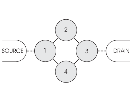
Our array system consists of four metallic or semiconducting islands, positioned as depicted in Fig. 1, between the source and the drain electrodes. Nearest-neighboring islands are connected by tunnel junctions so that there are two conducting paths between the source and the drain: upper one via the top island (island 2) and lower one via the bottom island (island 4). Let us assign and for the tunnel-junction capacitance and resistance, respectively, and for the cross-island capacitance (between islands 1 and 3 and between islands 2 and 4). Furthermore, each island is capacitatively coupled to the ground with same capacitance . The capacitance matrix is then written as
| (1) |
where and .
When a constant voltage is applied between the source and the drain and charges are there on island ( is an integer), the potential of island is given by, in the matrix form,
| (2) |
where the column vector is defined by
| (3) |
where . By inverting the capacitance matrix given by Eq. (1), we have
| (4) |
where
| (5) | |||||
| (6) | |||||
| (7) |
where
| (8) | |||||
| (9) | |||||
| (10) |
and
| (11) |
The current is calculated for the constant applied voltage by using the standard Monte Carlo (MC) method with the transition rates determined by the Golden-rule;[3, 5] the transition rate for a single-electron tunneling over a junction is given by
| (12) |
where is the free energy change by the tunneling event. The free energy consists of the electrostatic energy contribution and the work done by the external voltage source as usual. One may conveniently obtain the free energy change by a tunneling process involving islands and through the relationship[5]
| (13) |
where and are potentials of th island before and after the tunneling, respectively. Since only one electron is involved in a single tunneling process, the charges on each island are changed by at most, so we can easily calculate via Eqs. (2)-(11) and Eq. (13).
We also used the master equation approach assisted by the MC method as follows, especially when rare events should be taken care of. The master equation[10, 11] is written as
| (14) |
where is the transition rate from state to state and is the probability of finding state among total states considered in the calculation. The states considered in Eq. (14) are composed of frequent states that are readily obtained by a MC run and of rare states, if necessary, which may have to be inserted manually with some physical reasoning if they are hardly visited by the MC runs. Eq. (14) is solved either iteratively or by directly solving the equilibrium-state equation:
| (15) |
where is a by matrix where and is the vector of the state probabilities. Since the matrix is singular, we take a sub-matrix of size by removing row and column from the full matrix . Then
| (16) |
where is obtained by
| (17) |
In the master equation approach, a priori knowledge about the relevant states is the key to the successful calculation.
We have also considered cotunneling[12] up to the second order. The reason that only up to the second-order is considered here is that we will be interested in cotunneling out of the stationary charge configuration, as will be discussed later, where the charges are trapped on the top (island 2) and bottom (island 4) islands of the array. The cotunneling rate is then given by the exact double-junction formula:[12]
| (18) | |||||
| (19) |
where and are the free energy changes for the intermediate tunneling processes which are involved in the cotunneling process, and is that for the cotunneling. In the above equation, , and and are the resistances of the junctions involved in the cotunneling process.
In this paper, the units of the current, voltage, and temperature are , , and , respectively.
III Results And Discussions
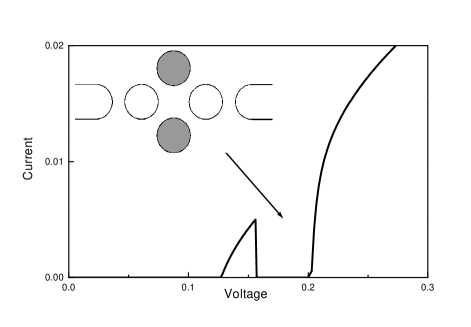
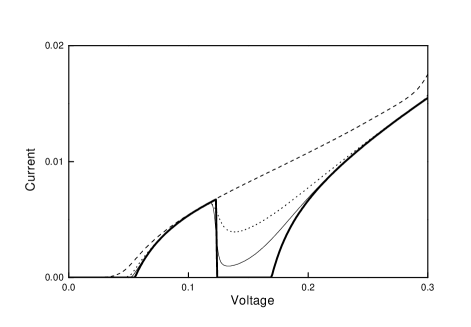
A unique feature in the characteristics of the four-island tunnel-junction array is the existence of another CB gap in a low voltage region at low temperatures,[8] as shown in Fig. 2. In the figure, where , , and , the SCB gap in the interval of is seen in addition to the primary CB gap in the interval of . The origin of the additional gap is attributed to the formation of the trapped-electron configuration or the stationary charge configuration (SCC) where two electrons trapped on the top and the bottom islands block the electrical conduction,[8, 9] as schematically shown in inset of Fig. 2.
A SCC is a local minimum of the free energy in the configuration space. That is, for each transition from the SCC to its adjacent configurations (the configurations which can be reached by a single-electron tunneling from the SCC) the free energy change ; otherwise, the electrons will not be trapped. In the following we will describe the properties of the SCCs in the four-island array.
A Stationary Charge Configurations
There are two SCCs that are noteworthy in the four-island array. The first one is the SCC with one trapped electron on island 1 (SCC-1). If we denote a charge configuration by where is the number of electrons on island , SCC-1 corresponds to . One of distinct features of the ring-shaped four-island array in contrast to the linear 1D arrays is the existence of the SCC-1. In linear 1D arrays of four islands with identical junctions, the tunneling process which triggers the conduction is ; once an electron tunnels onto the first island connected to the source, it has no problem in tunneling through the array. More specifically, let us denote as the threshold voltage for entrance of one electron onto the array (; let us denote the free energy change of the process by ) and as the threshold voltage for the electron to move forward (). In linear 1D arrays, , which implies that at the threshold voltage , the free energy change is already less than zero, so the threshold voltage for electrical conduction is in that case. In the ring-shaped four-island array, however, , as will be seen shortly, which implies that there is a range where the SCC-1 persists.[13]
and of our four-island array are given by, using Eqs. (2)-(11) and Eq. (13),
| (20) | |||||
| (21) |
and
| (22) | |||||
| (23) |
The threshold voltages and are zeros of the above free energy differences. For (the strong screening case), for simplicity, we get from Eqs. (21) and (23)
| (24) |
and
| (25) |
From Eqs. (24) and (25), one can easily see that for all . The same is true for arbitrary . We thereby show that SCC-1 exists in the bias-voltage range of in our four-island array.
The second SCC, which is at the heart of our discussion here, is the one with two trapped electrons on islands 2 and 4 (SCC-2), whose charge configuration is . To investigate the formation and destruction of the SCC-2, we need to consider following two tunneling processes: 1) the tunneling process which leads to onset of the SCC-2 (once the configuration is reached, the desired stationary configuration will be eventually reached from there because the tunneling process is a frequent process) and 2) the tunneling process (or, equivalently, ) which leads to break-up of the SCC-2. Let us denote the free energy changes of the former and the latter tunneling processes as and , respectively. Then,
| (26) | |||||
| (27) |
and
| (28) | |||||
| (29) |
At the threshold voltage where of Eq. (27) becomes zero, a second electron can now enter the array, and after subsequent tunneling events, the charge configuration will be eventually reached. From the configuration, the only possible tunneling process is (or equivalently, ). If the free energy change for the process is greater than zero, the tunneling process is energetically unfavorable so that the electrons get trapped and consequently the SCC-2 is established. See Fig. 3. Thus the necessary condition for the formation of the SCC-2 is , where is the zero of .
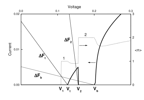
There are two tunneling processes which lead to destruction of the SCC-2. The first one is the tunneling process where the trapped electrons are forced to move forward: which is energetically favorable if , that is, if . The other one is the tunneling process which introduces a third electron into the array: , which is energetically possible only when , where is the threshold voltage for the process. Therefore, the SCC-2 persists in the voltage range .
Therefore, the SCC-2 is established if the following condition is satisfied:
| (30) |
Then a current peak in the voltage interval of and the SCB gap in the interval of will be seen in the at zero temperature.
Let us now discuss when the condition of Eq. (30) holds. For , for simplicity, threshold voltages , and are given by
| (31) | |||||
| (32) |
and
| (33) |
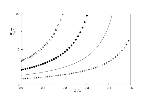
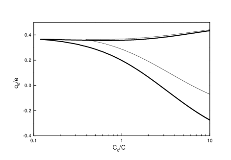
where . From Eqs. (25) and (31)-(33), we obtain that the equality of Eq. (30) is satisfied if . In general, when the cross capacitance is nonzero, the expressions for the threshold voltages are much more complex than in the strong screening case, and one has to resort to numerical calculation for the evaluation of the equality of Eq. (30). In Fig. 4, we show , the critical value of for the observation of the secondary Coulomb blockade gap, with respect to the screening factor . The figure shows that as the cross capacitance increases also increases.
In summary, we have shown that the SCC-1 exists in the range and the SCC-2 may exist in the range , if the condition is satisfied. The regions and are zero-current regions, but in between the two regions, the current flows such that it appears in the characteristics that the SCB gap shows up in the range . In terms of number of trapped electrons , we observe that the system becomes conducting during the transition from = 1 to 2 (see Fig. 3 where the average number of electrons inside the array is also shown). Noting that both the SCC-1 and the SCC-2 are stable charge configurations in time, we remark that the reason that the system becomes conducting during the transition is that dynamically unstable charge configurations in time must be passed en route. If we start with the SCC-1 and try to reach the SCC-2, the charges should physically move in the meantime and they keep tunneling through the array until the charges are balanced as required by the geometry of the array (or electrostatic force). In short, the SCB gap results because the topology of our ring-shaped array makes it possible that unstable conducting state exists between two stable insulating states. For the array of larger size having the same topology (i.e. the array with two branches between the source and the drain), this behavior is further generalized: that is, the current peaks can appear during each transition from odd to even .[9] We have reported in Ref. [9] that three peaks can be observed for the array of 60 islands, during each transition of = , , and . The reason that the current peaks arise only when changes from odd to even is that the transition from even to odd does not involve unstable charge states during the transition.
B Effect of Uniform Background Charges
We have so far dealt with the system with neutral background charge on each island: i. e. in Eq. (3). A uniform background charge on each island may be induced by attaching a (metallic) plate close to the array and applying a voltage between the plate and the ground. Then in Eq. (3),
The effect of the uniform background charge on the threshold voltages introduced above is to shift them by a certain amount linearly proportional to but at different rates for different threshold voltages. For example, the threshold voltages and become:
| (34) | |||||
| (35) |
Therefore, if we vary in the range , we may tune it such that the equality in Eq. (30) is satisfied. In Fig. 5, we show the domain in the plane of and where the SCB gap can be observed at zero temperature for the cases and 1/4; the region enclosed by two thick solid lines represents the domain where the SCB gap is observed at zero temperature for , and that enclosed by two thin solid lines for . Fig. 5 indicates that for , the SCB region is readily accessible by adjusting the (gate) plate voltage . The region becomes wider as becomes larger, but if is too big () the SCB gap shrinks, as does the usual Coulomb gap, and the current peak between them becomes too narrow to be observed. We thus find that the range of is practically the range where the SCB gap can be observed, by adjusting the gate voltage . Fig. 5 also shows that the effect of the screening factor is to shrink the domain. That the domain shrinks with respect to the increase of may be understood by noting that, if the interaction between the top (2) and bottom (4) islands increases by the increase of , the stationary charge configurations are harder to be built up, so one needs less coupling between islands, by having bigger , to compensate the increase in the interaction between the islands.
C Effect of Fluctuations
We have so far investigated the SCB phenomena when the temperature is zero and the quantum tunneling is suppressed. In the fluctuation-free case, the existence of the SCB gap results from the fact that the SCC with two trapped electrons is a stable configuration. The thermal and/or quantum fluctuations will, however, destabilize the SCC, so that the SCB gap will be transformed into a NDR region or entirely disappear, depending on the degree of the fluctuations. We will first discuss the effect of the temperature as follows.
At finite temperature , the trapped electrons in the SCC-2 have a probability to tunnel forward onto the island 3:
| (36) |
The average time that it takes for the tunneling event to occur is . (Tunneling out of both of the islands 2 and 4 contributes to the factor of two.) That is, after on average, the SCC-2 is broken down by tunneling of one of trapped electrons onto island 3. The electron subsequently exits through the drain, provoking a series of tunneling events to take place before the SCC-2 is restored, and the sequence of break-up and restoration of the SCC-2 is repeated. Let us denote as the time that it takes for the SCC-2 to be restored after it is broken down and as the amount of charges that are transfered through the array meanwhile. The current through the array is then given by
| (37) | |||||
| (38) |
where is approximately the current that would flow through the array if the SCC-2 would not have been formed in the first place: i. e. the current which would fill the SCB gap smoothly (see Fig. 6). Since at low temperatures,
| (39) |
Therefore, for , the SCB gap at zero temperature is transformed into a NDR region and for , the SCB gap entirely disappears and the current increases monotonically with respect to the bias voltage. See Fig. 6. We estimate that , which implies that for the junction capacitance of the order of 1 aF, 1 K.
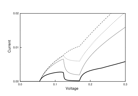
The second source of fluctuations is cotunneling. It is energetically favorable that the trapped electrons in the SCC-2 cotunnel onto the drain electrode. The cotunneling rate is given by Eq. (19) with , and . Once the cotuneling event occurs, the same sequence of break-up and restoration of the SCC-2 takes place as in the case of the thermal fluctuation. The current is then given by Eq. (38) with replaced by . Since , where is the resistance of the junction between island 3 and the drain, one roughly has . Therefore, as in the case of the thermal fluctuation, there exist a certain above which the SCB gap is transformed into a NDR region and below which the characteristics show monotonic increase. See Fig. 7. We estimate that .
It may be worthwhile to discuss on how cotunneling was incorporated in our calculation of the current in a little more detail. The current in the SCB gap was obtained by solving the master equation with the cotunneling process mentioned above included. As an alternative way, we evaluated Eq. (38) with replaced by and by independently measuring through MC runs. Both of the results agreed very well. Using the cotunneling rate given by Eq. (19) in the two methods poses no difficulty in calculations in the SCB gap (). Beyond the gap (), however, diverges because of the occurrence of sequential tunnelings in parallel. Therefore we used the approximation by Jensen and Martinis[14] to calculate the current beyond the gap and adjusted thus-obtained current curve so as for the current to be continuous at the threshold voltage . This method of ours is far from being a rigorous one but may be justified because we are only interested in the effect of cotunneling in the SCB gap region for which we have treated the problem more carefully.
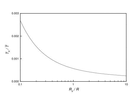
Discussing both the thermal and the quantum fluctuations separately, we can now address the crossover temperature between the quantum-fluctuation dominant regime and the thermal-fluctuation dominant regime: for (the quantum regime), the currents are virtually unchanged with respect to the temperature but (the classical regime), the currents monotonically increase with increase of temperature. We may estimate by equating the normal transition rate and the cotunneling rate at a bias voltage for which we take the middle point of the SCB gap. Fig. 8 shows thus-estimated crossover temperatures versus the junction resistance for the case of , , and . As is expected, as the junction resistance increases, the crossover temperature decreases in the figure, which implies that the quantum fluctuations become less effective as increases.
D Effect of Disorders
Let us now discuss how rigid the SCB gap is against possible imperfection of the array. Mainly there are three sources of disorder in real experiments: 1) the size of the islands may differ from one another, 2) the positions of the islands could be somewhat away from the desired ones, and 3) the stray charges may be induced on each island. Before we remark on the effect of the disorders in general, let us take a specific example to demonstrate the effect of the stray charges, among others. Note that stray charges on islands 2 and 4 may substantially affect the formation of the SCC-2 because the charges should be trapped there. When the background charge of island 2 differs from that of other islands by , the threshold voltage changes by
| (40) |
and, regardless of the sign of , changes by
| (41) |
The change in the threshold voltage is immaterial in the discussion here. Eqs. (40)-(41) show that the SCB gap shrinks linearly with respect to . The SCB gap will be still seen if the change , and we find that the range in for which the SCB gap persists is typically around 0.1. But the SCB gap is much more vulnerable to negative stray charges than positive ones, which reflects the fact that a negatively charged electron is harder to get trapped if the island is more negatively charged. If we can adjust the overall background charges on each island, in the direction to compensate the stray charge, we may be able to re-enter the region where the SCB gap is seen.
We found it a challenging task to treat the problem analytically when the disorders are present in general, so we resorted to numerical simulations with the following simple model. The first two sources of imperfection mentioned above may be treated by relaxing the condition of having identical islands and allowing the mutual capacitances to have ‘random’ contributions to some degree as follows:
| (42) |
where refers to the capacitance between island and (including the source, the ground, and the drain electrodes), is a constant adjusting the magnitude of the randomness and ’s are random numbers between -1/2 and 1/2. Note that in the above equations, we have specifically put the subscripts for to note that the random numbers are differently assigned for different islands and different pairs of islands. Similarly, for the third source of imperfection, we may introduce random contributions to of each island. Our numerical simulations show that for up to 10 % of random contributions the SCB phenomena is still observed, although the SCB gap position or the NDR region is shifted and/or its width is changed.
IV Conclusion
In conclusion, we have shown that the secondary Coulomb blockade gap of the four-island array at zero temperature is originated from the property of the array that it traps up to two electrons inside, due to its unique topology. The detailed tunneling mechanism which leads to the formation and destruction of the stationary charge configuration with two trapped electrons inside, which corresponds to the additional gap, has been analyzed. We have also considered the effect of the thermal and quantum fluctuations on the gap, and found that the gap transforms into a NDR region upon introduction of the fluctuations. The NDR feature suggests a potential application of the ring-shaped array as a diode showing the NDR behavior. We have also studied the effect of the uniform background charges on each island, which can be realized in real experiments by attaching a ground plate near the array and applying a voltage, and found that the secondary Coulomb blockade gap is more readily accessible by adjusting the voltage. Based on the detailed analysis that we have carried out in this study, the physical properties of the multiple Coulomb gaps of larger size array may be similarly understood.
The authors thank Gwang-Hee Kim for fruitful discussions on the cotunneling effect and the crossover temperature. This work has been supported by the Ministry of Information and Communications of Korea.
REFERENCES
- [1] E-MAIL: mcshin@etri.re.kr
- [2] Among others, K. K. Likharev, IBM J. Res. Dev. 32, 144 (1988); G. L. Ingold and Yu. V. Nazarov, in Single Electron Tunneling, edited by H. Grabert and M. H. Devoret (Plenum, New York, 1991), p. 21; P. Delsing, ibid, p. 249.
- [3] M. Amman, E. Ben-Jacob and K. Mullen, Phys. Lett. A 142, 431 (1989).
- [4] G. Y. Hu and R. F. O’Connell, Phys. Rev. B 49, 16773 (1994).
- [5] N. S. Bakhvalov, G. S. Kazacha, K. K. Likharev and S. I. Serdyukova, Zh. Eksp. Teor. Fiz. 95, 1010 (1989) [Sov. Phys. JETP 68, 581 (1989)]; K. K. Likharev, N. S. Bakhvalov, G. S. Kazacha and S. I. Serdyukova, IEEE Trans. Magn. 25, 1436 (1989).
- [6] C. B. Whan, J. White and T. P. Orlando, Appl. Phys. Lett. 68, 2996, (1996).
- [7] K. K. Likharev and K. A. Matsuoka, Appl. Phys. Lett. 67, 3037 (1995).
- [8] M. Shin, S. Lee, K. W. Park and E.-H. Lee, to be published in J. Appl. Phys. (1998).
- [9] M. Shin, S. Lee, K. W. Park and E.-H. Lee, Phys. Rev. Lett. 80, 5774 (1998).
- [10] D. V. Averin and K. K. Likharev, in it Mesoscopic Phenomena in Solids, edited by B. L. Altshuler, P. A. Lee, and R. A. Webb (Elsevier, Amsterdam, 1991), p. 173.
- [11] L. R. C. Fonseca, A. N. Korotkov, K. K. Likharev, and A. A. Odintsov, J. Appl. Phys. 78, 3238 (1995).
- [12] D. V. Averin and Yu. V. Nazarov, in it Single Electron Tunneling, edited by H. Grabert and M. H. Devoret (Plenum, New York, 1991), p. 217, and references therein.
- [13] In general, the tunneling process which leads to the conduction of the four-island array is not necessarily the one mentioned in the text. For lower values of (), for instance, two electrons get trapped on islands 1 and 3 initially, and the tunneling process which trigers the conduction is either the one where the trapped electron on island 3 exits through the drain or the one where the trapped electron on island 1 advances forward. When the uniform background charges are induced on each island, as will be discussed later, the situation becomes very complicated. However, for the range of that we are interested in in this paper, the tunneling process mentioned in the text is the one responsible for the conduction.
- [14] H. D. Jensen and J. M. Martinis, Phys. Rev. B 46, 13407 (1992).