Josephson-Junction Qubits and the Readout Process by Single-Electron Transistors
Abstract
Several physical realizations of quantum bits have been proposed, including trapped ions, NMR systems and spins in nano-structures, quantum optical systems, and nano-electronic devices. The latter appear most suitable for large-scale integration and potential applications. We suggest to use low-capacitance Josephson junctions, exploiting the coherence of tunneling in the superconducting state combined with the possibility to control individual charges by Coulomb blockade effects. These systems constitute quantum bits (qubits), with logical states differing by one Cooper-pair charge. Single- and two-bit operations can be performed by applying a sequence of gate voltages. The phase coherence time is sufficiently long to allow a series of these steps. The ease and precision of these manipulations depends on the specific design. Here we concentrate on a circuit which is most easily fabricated in an experiment.
In addition to the manipulation of qubits the resulting quantum state has to be read out. This can be accomplished by coupling a single-electron transistor capacitively to the qubit. To describe this quantum measurement process we study the time evolution of the density matrix of the coupled system. Only when a transport voltage is turned on, the transistor destroys the phase coherence of the qubit; in this case within a short time. The measurement is accomplished after a longer time, when the signal resolves the different quantum states. At still longer times the measurement process itself destroys the information about the initial state. We present a suitable set of system parameters, which can be realized by present-day technology.
I Introduction
The investigation of nano-scale electronic devices, such as low-capacitance tunnel junctions or quantum dot systems, has always been motivated by the perspective of future applications. By now several have been demonstrated, e.g. the use of single-electron transistors (SET) as ultra-sensitive electro-meters and single-electron pumps. From the beginning it also appeared attractive to use these systems for digital operations needed in classical computation (see Ref. [1] for a review). Obviously single-electron devices would constitute the ultimate electronic memory. Unfortunately, their extreme sensitivity makes them also very susceptible to fluctuations and random background charges. Due to these problems — and the continuing progress of conventional techniques — the future of SET devices in classical digital applications remains uncertain.
The situation is different when we turn to elements for quantum computers. They could perform certain calculations which no classical computer could do in acceptable times by exploiting the quantum mechanical coherent evolution of superpositions of states [2]. Here conventional systems provide no alternative. In this context, ions in a trap, manipulated by laser irradiation are the best studied system [3, 4]. However, alternatives need to be explored, in particular those which are more easily embedded in an electronic circuit. From this point of view nano-electronic devices appear particularly promising.
The simplest choice, normal-metal single-electron devices are ruled out, since — due to the large number of electron states involved — different, sequential tunneling processes are incoherent. Ultra-small quantum dots with discrete levels, and in particular, spin degrees of freedom embedded in nano-scale structured materials are candidates. They can be manipulated by tuning potentials and barriers [5]. However, these systems are difficult to fabricate in a controlled way. More attractive appear systems of Josephson contacts, where the coherence of the superconducting state can be exploited and the technology is quite advanced. Macroscopic quantum effects associated with the flux in a SQUID have been demonstrated [6]. Quantum extension of elements based on single flux logic have been suggested [7, 8], and efforts are made to observe one of the elementary processes, the coherent oscillation of the flux between degenerate states [9].
We have suggested [10] to use low-capacitance Josephson junctions, where Cooper pairs tunnel coherently while Coulomb blockade effects allow the control of individual charges. They provide physical realizations of quantum bits (qubits) with logical states differing by the number of Cooper pair charges on an island. These junctions can be fabricated by present-day technology. The coherent tunneling of Cooper pairs and the related properties of quantum mechanical superpositions of charge states have been discussed and demonstrated in experiments [11, 12, 13, 14, 15, 16]. In particular, in a recent experiment [17] Nakamura et al. have observed time-resolved coherent oscillations of charge in such Josephson junction setup.
We concentrate here on the simplest design of the qubit, which is sufficient to introduce the ideas, and it is most easy for fabrication. It should be added that other ideas in this direction have been discussed [18, 19]. In Ref. [19] an improved design has been proposed that relaxes requirements to the parameters of the circuit and makes the manipulation procedures more flexible. In Section II we will introduce the system and show how single- and two-bit operations (gates) can be performed by the application of sequences of gate voltages. In Section III we analyze the influence of dissipation and fluctuations and conclude that for a proper choice of parameters the phase coherence time is sufficiently long to allow a large number of gate operations.
In addition to the controlled manipulations of qubits, quantum computation requires a quantum measurement process to read out the final state. The requirements for both steps appear to contradict each other. During manipulations the dephasing should be minimized, whereas a measurement should dephase the state of the qubit as fast as possible. The option to couple the measuring device to the qubit only when needed is hard to achieve in nano-scale systems. The alternative described in Section IV, is to couple a normal-state single-electron transistor capacitively to a qubit [20]. During the manipulations the transport voltage of the SET is turned off, and the SET only acts as an extra capacitor. To perform the measurement the transport voltage is turned on. The dissipative current through the transistor dephases the qubit and provides the read-out signal for the quantum state. We describe this quantum measurement process by considering explicitly the time-evolution of the density matrix of the coupled system. We find that the process is characterized by three time scales: a short dephasing time, the longer ‘measurement time’ when the signal resolves the different quantum states, and finally the mixing time after which the measurement process itself destroys the information about the initial state. Similar nonequilibrium dephasing processes [21, 22, 23] have recently been demonstrated experimentally [24].
In Section V we discuss system parameters and suggest suitable sets which can be realized by present-day technology. We further compare with related work.
II Josephson junction qubits
A Qubits and single-bit gates
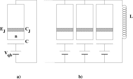
The simplest Josephson junction qubit is shown in Fig. 1a. It consists of a small superconducting island connected by a tunnel junction, with capacitance and Josephson coupling energy , to a superconducting electrode. An ideal voltage source, , is connected to the system via a gate capacitor (fluctuation effects will be discussed later). We choose a material such that the superconducting energy gap is the largest energy in the problem, larger even than the single-electron charging energy to be discussed below. In this case quasi-particle tunneling is suppressed at low temperatures, and a situation can be achieved where no quasiparticle excitations exist on the island***Under suitable conditions the superconducting state is totally paired, i.e. the number of electrons on the island is even, since an extra quasi-particle (odd number of electrons) costs the extra energy . This ‘parity effect’ has been established in experiments below a crossover temperature , where is the number of electrons in the system near the Fermi energy [13, 25, 26, 27]. For a small enough island, is typically one order of magnitude smaller than the superconducting transition temperature. For the case that — e.g. due to the initial preparation — an unpaired excitation exists on the island, a channel should be provided for the quasiparticle to escape to normal parts of the system [25]..
In the following we will consider the situation where only Cooper pairs tunnel in the superconducting junction. This system is described by the Hamiltonian
| (1) |
Here, is the number (operator) of extra Cooper pair charges on the island (relative to some neutral reference state) and the phase variable is its conjugate . The charging energy of the superconducting island is characterized by the scale , while the dimensionless gate charge, , acts as a control field. We consider systems where is much larger than the Josephson coupling energy, . In this regime a convenient basis is formed by the charge states, parameterized by the number of Cooper pairs on the island. In this basis the Hamiltonian (1) reads
| (3) | |||||
For most values of the energy levels are dominated by the charging part of the Hamiltonian. However, when is approximately half-integer and the charging energies of two adjacent states are close to each other, the Josephson tunneling mixes them strongly (see Fig. 2).

We concentrate on the voltage interval near a degeneracy point of two charge states, say and . For the parameters chosen, further charge states can be ignored, and the system (1) reduces to a two-state model, with Hamiltonian which can be written in spin- notation in terms of Pauli spin matrices as
| (4) |
The charge states and correspond to the spin basis states and , respectively. The charging energy , equivalent to a magnetic field in -direction in the spin problem, is controlled by the gate voltage. For convenience we can further rewrite the Hamiltonian as
| (5) |
where the mixing angle determines the direction of the effective magnetic field in the -plane, and the energy splitting between the eigenstates is . At the degeneracy point, , it reduces to . The eigenstates are denoted in the following as and . For some chosen value of they are
| (6) | |||||
| (7) |
For later convenience we can rewrite the Hamiltonian in the basis of eigenstates. To avoid confusion we introduce a second set of Pauli matrices, , which operate in the basis and , while reserving for the basis of charge states and . By definition the Hamiltonian then becomes .
By changing the gate voltage we can perform the required one-bit operations (gates). If, for example, one chooses the idle state far away from degeneracy, the eigenstates and are close to and , respectively. For definiteness, we choose the eigenstates and at the idle point as logical basis states. Then switching the system suddenly to the degeneracy point for a time and then switching back produces a rotation in spin space,
| (8) |
where . Depending on the value of , a spin flip can be produced, or, starting from , a superposition of states with any chosen weights can be reached. This is exactly the way the experiments of Nakamura et al. [17] were performed. At the same time, keeping the system at the idle point we achieve a phase shift between two logical states by the angle . A different phase shift during the same time period can be achieved using a temporary change of by a small amount which changes the energy difference between the ground and excited states.
The example presented above provides an approximate spin flip for the situation where the idle point is far from degeneracy and . But a spin flip in the logical basis can also be performed exactly. It requires that we switch from the idle point to the point where the effective magnetic field is orthogonal to the idle one, . This changes the Hamiltonian from to . To achieve that, the dimensionless gate charge should be increased by . In the limit discussed above, , the operating point is close to the degeneracy, .
Unitary - and -rotations described above are sufficient for all manipulations with a single qubit. By using a sequence (of no more than three) such elementary rotations we can achieve any unitary transformation of the qubit’s state.
In our discussion so far elementary rotations should have been performed one immediately after another. However, sometimes the quantum state should be kept intact for a certain time interval, for instance, while other qubits are manipulated during the computation. Even in the idle state , the energies of the two eigenstates are different. Hence their phases evolve relative to each other, which leads to the quantum mechanical ‘coherent oscillations’ of a system which is in a superposition of eigenstates. We have to keep track of this time dependence as is demonstrated by the following example (for simplicity again on the approximate level). Imagine we try to perform a rotation by angle in the spin space, which we can do by a suitable choice of in (8), and after some time delay we perform the reverse operation. The unitary transformation for this combined process is
Clearly the result depends on the intermediate time and differs from unity or a simple phase shift, unless . The time-dependent phase factors, arising from the energy difference in the idle state, can be removed from the eigenstates if all the calculations are performed in the interaction representation, with zero-order Hamiltonian being the one at the idle point. In this way the information which is contained in the amplitudes of the qubit’s states is preserved. However, there is a price for this simplification, namely the transformation to the interaction representation introduces additional time dependence in the Hamiltonian during the operations. Thus a general 1-bit operation induced by switching at from to for some time is described by the unitary transformation
| (9) |
This demonstrates that the effect of the operations depends not only on their time span but also on the moment when they start.
The transformation (9) is the elementary operation in the interaction picture in the sense that it can be performed in one step (one voltage switching). Can we perform an arbitrary single-bit gate using such an operation? To answer this question we note that all the unitary transformations of the two-state system form the group SU(2). The group is three-dimensional, hence one needs in general three controllable parameters to obtain a given single-bit operation. As is obvious from (9), depends exactly on three parameters: , and . It can be shown that any single-bit gate can be performed in one step if the voltage (i.e. ) and the times , are chosen properly.†††It is customary to consider rotations about two axes, say, - and -rotations, as device-independent elementary single-qubit gates. Then, any single-bit gate in a quantum algorithm is described as a combination of three consecutive elementary rotations given by their angles (e.g. Euler angles , , ). To realize such a gate we need to solve the equation to find the triple of , and . Since usually only a few different single-bit gates are used, corresponding triples can be calculated in advance. (The dependence on is periodic with the period . Hence the waiting time to a new operation is restricted to this period.)
As a final remark in this subsection, we notice that our choice of the logical basis is by no means unique. As follows from the preceding discussion, we can perform - and -rotations in this basis, which provides sufficient tools for any unitary operation. On the other hand, since we can perform any unitary transformation, we can as well perform - and -rotations in any basis of our two-dimensional system. Therefore, any basis can serve as the logical one. The Hamiltonian at the idle point is diagonal in the basis (6), while the controlled part of the Hamiltonian, the charging energy favors the charge basis. For this reason manipulation procedures for - and -rotations, in the interaction representation, are of comparable simplicity in all bases. The preparation procedure (thermal relaxation at the idle point) is easier described in the eigenbasis, while coupling to the meter (see Section IV) is diagonal in the charge basis. So, there is no obvious choice for the logical states and it is a matter of convention.
B Many-qubit system
For quantum computation a register, consisting of a (large) number of qubits is needed, and pairs of qubits have to be coupled in a controlled way. Such two-bit operations (gates) are necessary, for instance, to create entangled states. For this purpose we couple all qubits by one mutual inductor as shown in Fig. 1b. One can easily see that for the system reduces to a series of uncoupled qubits, while for they are coupled strongly. Finite values of introduce some retardation in the interaction. The Hamiltonian of this system, consisting of qubits and an oscillator formed by the inductance and the total capacitance of all qubits is [10]
| (10) | |||||
| (11) |
Here is the flux in the mutual inductor, is the flux quantum, and , the variable conjugated to , is related to the total charge on the gate capacitors of the qubits. For the oscillations in this -circuit the junction and gate capacitor of each qubit act in series, hence the relevant capacitance is . The voltage oscillations of the -circuit affect all the qubits equally, thus is coupled to each of the phases . The reduction factor describes the screening of these voltage oscillations by the gate capacitors. Here we have chosen to express the coupling via a shift of the phase in the Josephson coupling terms arising from the voltage oscillations. This form is reminiscent of the usual description of SQUIDs, except that is a dynamic variable and its effect is reduced by the ratio of capacitances. Alternatively, we could have added the oscillating charges to the gate charges in the charging energy. Both forms are equivalent and related by a canonical transformation. This and a more detailed derivation of (11) has been presented in Ref. [10].
The oscillator described by the charge and flux with characteristic frequency produces an effective coupling between the qubits. We choose parameters such that
| (12) | |||||
| (13) |
The first condition (12) assures that the oscillator remains in its ground state at all relevant operation frequencies. I.e. the logical operations on the qubits are not affected by excited states. The second condition (13) prevents the Josephson coupling in (11) from being “washed out” by the fluctuations of . Since they are limited by , hence , this condition imposes only weak constraints on the parameters.
Although the -oscillator remains in its ground state, it provides an effective coupling between the qubits. To analyze this we expand in (11) the Josephson coupling terms in and, because of (13), neglect powers higher than linear. The linear term is , where the current through the inductor is given by the sum of qubits’ contributions,
| (14) |
The linear term and the unperturbed Hamiltonian of the oscillator can be combined to a square,
| (15) |
As long as the frequency of the oscillator is large compared to characteristic frequencies of the qubit’s motion (12), one can use the adiabatic approximation and treat the slow qubit’s variables () as constant to find the energy levels of the oscillator. Since the lowest level of the first two terms in the rhs of Eq.(15), equal to , does not depend on , the correction to the ground state energy is given by the last term. This term provides the effective coupling between the qubits
| (16) |
where the energy scale is
| (17) |
In the spin- notation and the interaction term becomes (up to constant terms)
| (18) |
The ideal system would be one where the coupling between different qubits could be switched on and off, leaving the qubits uncoupled in the idle state and during 1-bit operations. This option requires a more complicated design [19]. With the present, simplest model the qubits are coupled at all times. But even in this case we can control the coupling in an approximate way by tuning the energies of the selected qubits in and out of resonance. If is smaller or comparable to and the gates voltages are all different, such that no two qubits are near a degeneracy, the interaction (18) has only weak effects. In this case, the eigenstates of, say, a two-qubit system are approximately , , and , separated by energies larger than . Hence, the effect of the coupling is weak. If, however, a pair of these states is degenerate, even a weak coupling lifts the degeneracy, changing the eigenstates drastically. For example, if , the states and are degenerate. In this case the correct eigenstates are: and with energy splitting between them.
With the coupling (18) we are able to perform two-bit operations and create, e.g., entangled states. In the idle state we bias all qubits at different voltages. Then we suddenly switch the voltages of two selected qubits to be equal, bringing those two qubits for a time into resonance, and then we switch back. The result is a two-bit operation, which is a rotation in the subspace spanned by :
| (19) |
where . The states merely acquire phase factors, relative to what they would acquire in the idle state. For all other qubits the interaction remains a small perturbation.
Similar to the situation with single-bit gates, the many-qubit states have time-dependent phase factors and the result of consecutive 2-bit gates depends on the waiting time between them. Again a transformation to the interaction representation makes this time dependence explicit. One can show that any two-qubit operation can, in principle, be performed exactly. However, the complexity of such exact manipulation grows with the number of qubits. The improved design proposed in [19] allows one to switch on and off the coupling between the qubits and to perform exact two-qubit operations in a simple way.
C Extensions and discussion
To check the experimental feasibility of the present proposal it is necessary to estimate the time-span of the voltage pulses needed for typical single-bit operations. We note that a reasonable value of is of the order of –1K. It cannot be chosen much lower, since the condition should be satisfied, and it should not be much larger since this would increase the technical difficulties associated with the time control. The corresponding time-span is nevertheless short, –ps, and is difficult to control in an experiment.
There exist, however, alternatives. On one hand, a controlled ramping of the coupling energy provides a well defined, though non-trivial single-bit operation. Since in general, any 1-bit gate can be performed with proper choice of 3 controlled parameters, a universal set of gates can be produced in this way. Another possibility is to follow the established procedures of spin resonance experiments. E.g. a coherent spin rotation can be performed as follows: The system is moved adiabatically to the degeneracy point. Then an ac voltage with frequency is applied. Finally, the system is moved adiabatically back to the idle point. The time-width of the ac-pulse needed, e.g., for a total spin flip depends on the ac-amplitude, therefore it can be chosen much longer then . Unfortunately, in comparison to the sudden switching, the slow adiabatic approach allows only a reduced number of operations during the phase coherence time.
Also the two-bit gates, instead of application of short voltage pulses, can be performed by moving the system adiabatically to a degeneracy point (say ), and then applying an ac voltage pulse in the antisymmetric channel .
To improve the performance of the device generalizations of the design of the qubits and their coupling may be useful. We mention here one which has been described in Ref. [19]. There we discuss a system where the Josephson coupling can be tuned to zero as well. This can be achieved by replacing each Josephson junction by a SQUID with two junctions, and controlling the effective coupling by an applied magnetic flux. While this design is more complicated to fabricate, it has considerable advantages: (i) In the idle state the Hamiltonian can be tuned to zero (), which removes the problem that the unitary transformations not only depend on the time span of their duration but also on the time when they are performed. (ii) The two-bit coupling is turned on only for those two qubits which have both . (iii) With only or non-zero, the unitary transformations depend in a simple way on the time integral of the corresponding Hamiltonian. Hence ramping the energies produces simple, well-defined gates. As a result of these improvements the manipulations can be performed with much higher accuracy.
III Circuit effects: dissipation and dephasing
A Johnson-Nyquist noise of the gate voltage circuit
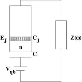
The idealized picture outlined above has to be extended to account for the possible dissipation mechanisms causing decoherence and relaxation. We focus on the dissipation and fluctuations which originate from the circuit of the voltage sources. In Fig. 3 the equivalent circuit of a qubit coupled to an impedance is shown. The latter is characterized by intrinsic voltage fluctuations (between its terminals when disconnected from the circuit), with spectrum
| (20) | |||||
| (21) |
When is embedded in a circuit, similar to that of Fig. 3 but with , the voltage fluctuations between the terminals of are characterized by a modified spectrum:
| (22) |
Here is the total impedance between the terminals of .
Following Caldeira and Leggett [28] we model the dissipative element by a bath of harmonic oscillators described by the Hamiltonian
| (23) |
It is assumed that the voltage between the terminals of is given by and the spectral function is chosen to reproduce the fluctuations spectrum (21), . Then, we embed the element in the qubit’s circuit and we use the Kirchhof constraints to derive the Hamiltonian of the whole system. Taking into account the possibility of a time-dependent external voltage , we arrive at the resulting Hamiltonian
| (24) | |||||
| (25) |
where the tilde-marking of the bath-related quantities reflects the fact that the bath has been modified and its spectral function corresponds now to the fluctuations spectrum (22), . Shifting the origins of all the oscillators , where is the time independent part of the external voltage, we get a more familiar form of the Hamiltonian:
| (26) | |||||
| (27) |
To be specific we will concentrate in the following on the fluctuations due to an Ohmic resistor in the bias voltage circuit.
B Relaxation and dephasing rates
In general, the environment has two effects: inelastic energy relaxation and dephasing, both characterized by their respective time scales, and . To illustrate this point we consider a qubit prepared in a superposition of eigenstates with non-vanishing coefficients and . This corresponds to an initial density matrix . In this case, one question is how fast the diagonal elements of the density matrix relax to their thermal equilibrium values. This relaxation is determined by . The second question is how fast the off-diagonal elements vanish, which is governed by the rate . In general, the two rates are not equal.
Both inelastic transitions and dephasing were addressed in the context of spin-boson models, in particular for a two-level system with purely Ohmic dissipation [29, 30]. Our system (27) reduces to a spin-boson model in the limit where only two charge states need to be considered, with a harmonic oscillator bath coupling to . It still differs from an Ohmic model due to the frequency dependence in the function . However, for the relevant frequencies, , the physics is dominated by the resistor. Hence we can take over the results from the model calculations of Refs. [29, 30] for purely Ohmic environments.
The strength of the fluctuations and, hence, the relaxation and dephasing effects are controlled by the resistance of the circuit. It turns out that it has to be measured in units of the quantum resistance k. Hence for low circuit resistances in the range of we can expect a weak effect. Furthermore, in our system the effect of fluctuation is reduced due to the weak capacitive coupling of the qubit to the circuit. Indeed, as is apparent from (27) the coupling of to the qubit’s charge involves the ratio . Thus, the relevant parameter characterizing the effect of the voltage fluctuations is .
In Ref. [29] only the unbiased case of the spin-boson model, corresponding to the qubit at the degeneracy point , has been analyzed rigorously in the limit of low dissipation (the only limit relevant for the quantum computation). The biased case of the spin-boson model at low dissipation (i.e. the qubit out of the degeneracy) was treated in Ref. [30]. The two rates, expressed in terms of the mixing angle introduced in (6), are
| (28) |
and
| (29) |
We note that out of the degeneracy the dephasing rate acquires a component proportional to the temperature. It should also be noted that the relaxation rate (28) may be obtained in a much simpler way [10] using the so called “” theory discussed in Refs. [31, 32, 33, 34].
Thus, the diagonal and off-diagonal elements in the basis of the qubit’s eigenstates relax with different rates described above, while the off-diagonal elements carry also an oscillating phase factor. The last is translated in the charge basis to the ‘coherent charge oscillations’, which are observed in the quantity . In the absence of dissipation this quantity oscillates coherently around some average value. With dissipation, this average value relaxes to equilibrium with rate , while the oscillations decay with rate [30].
The factors and in Eqs. (28,29) indicate the nature of different contributions to the relaxation and dephasing rates. In the basis of the eigenstates (6) the qubit’s part of the Hamiltonian (27) is diagonal. However, the circuit electromagnetic fluctuations couple to the charge. Hence, in the notation introduced after (6) we have
| (30) | |||||
| (31) |
Since the first term commutes with the qubit’s Hamiltonian, only the second one in (30) contributes to the transitions between the eigenstates. This explains the factor in (28). The first term in (30), while ineffective for transitions, makes the energy difference between the qubit’s levels fluctuate. Therefore, the off-diagonal elements of the density matrix acquire a random phase. The last process is “pure” dephasing. It occurs even when transitions are suppressed (e.g. when ). This particular case (, ) is quite simple and we can reproduce Eq. (29) in an exact calculation, examining also the zero temperature limit. To do this, we note that in the two state approximation the off-diagonal element of the reduced density matrix is given by . To calculate it we perform a canonical transformation , , after which the Hamiltonian (27) becomes:
| (32) | |||||
| (33) | |||||
| (34) |
The Josephson and the last terms are zero in our case and the evolution of {} is decoupled from the bath. In the two state approximation () the equations of motion read: , , where was introduced in Eq. (4). Thus, introducing , we get
| (35) | |||
| (36) | |||
| (37) |
The correlator was studied extensively by many authors [31, 32, 33, 34]. It is equal to , where
| (38) | |||
| (39) |
Since , we may roughly substitute the bath’s spectrum by a purely Ohmic one with a cut-off set at . Then, at non-zero temperature, for , and we reproduce Eq. (29) in the limit . At zero temperature for . Thus, the fact that the “pure” dephasing rate vanishes at zero temperature does not mean that there is no dephasing at all. The decay of the off-diagonal element of the reduced density matrix is just non-exponential but rather algebraic (see Refs. [35, 36]).
We conclude that the dephasing of the initial quantum state of the qubit is caused by two different processes: the dissipative transitions between the eigenlevels, and the fluctuations of the energy difference between the levels. The off-diagonal elements of the density matrix are suppressed by both of them. While the first process survives at low temperature, the second one produces the dephasing rate proportional to the temperature.
These results should be taken into account when selecting the optimum idle state for the qubit. If the temperature is low, , the best choice is obviously far from the degeneracy point (). Also at higher temperatures this regime has a longer coherence time than the degeneracy point, although only by a numerical factor. In all cases it is pure dephasing, rather than inelastic transitions which limits the coherence at the idle point.
C Discussion and extensions
In summary, the dephasing rate is small if the effective resistance of the circuit is low compared to the quantum resistance, . Furthermore, a low gate capacitance reduces the coupling of the qubit to the environment. Hence, with suitable parameters () at low temperatures the number of operations which can be performed before the environment destroys the phase coherence may be as large as –. The value of the phase coherence time in this case is of the order of 10–100 ns. Coherence times of this order of magnitude have been observed in experiments on quantum dots [37].
Longer phase coherence times would be achieved if the coupling of the qubit to the noisy environment could be further reduced, without weakening the coupling to the common inductor which provides the 2-bit coupling. The model discussed above is not ideal since the Ohmic resistor with Johnson-Nyquist noise is assumed to be in the immediate vicinity of the qubit, reduced in its effect only by a low gate capacitor. A suitable design with a combination of superconducting leads and filters can drastically improve the situation.
If the physical dephasing effects are reduced, the more serious will be the errors related to imperfections in the time control or imprecise parameters and coupling energies, e.g., non-vanishing 2-bit couplings during the idle periods. If the combination of all these effects is sufficiently reduced, allowing for – coherent manipulations steps, then eventually the remaining errors can be corrected by suitable codes [38]. It appears from our analysis that this goal can be reached with Josephson junction qubits.
IV Measuring the state of the qubit
A The model for a single-electron transistor attached to the qubit
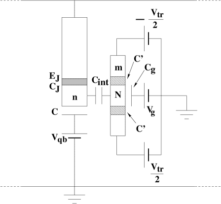
The read-out of the state of the qubit requires a quantum measurement process. Since the relevant quantum degree of freedom is the charge of the qubit island, the natural choice of measurement device is a single-electron transistor (SET). This system is shown in Fig. 4. The left part is the qubit, with state characterized by the number of extra Cooper pairs, , on the island, and controlled by its gate voltage, . The right part shows a normal island between two normal leads, which form the SET. It’s charging state is characterized by the number of extra single-electron charges on the middle island, . It is controlled by gate and transport voltages, and , and further, due to the capacitive coupling to the qubit, by the state of the latter. A similar setup has been studied in the experiments of Refs. [11] with the purpose to demonstrate that the ground state of a single Cooper pair box is a coherent superposition of different charge states. We will discuss the relation of these experiments to our proposal below.
During the quantum manipulations of the qubit the transport voltage across the SET transistor is kept zero and the gate voltage of the SET is chosen to tune the island away from degeneracy points. Therefore no dissipative currents flow in the system, and the transistor merely modifies the capacitances of the system. To perform a measurement one tunes the SET by to the vicinity of its degeneracy point and applies a small transport voltage . The resulting normal current through the transistor depends on the charge configuration of the qubit, since different charge states induce different voltages on the middle island of the SET transistor. In order to investigate whether the dissipative current through the SET transistor allows us to resolve different quantum states of the qubit, we have to discuss various noise factors, including the shot noise associated with the tunneling current and the measurement induced transitions between the states of the qubit. For this purpose we analyze the time evolution of the density matrix of the combined system. We find that for suitable parameters, which can be realized experimentally, the dephasing by the passive SET is weak. When the transport voltage is turned on the dephasing is fast, and the current through the transistor — after a transient period — provides a measure of the state of the qubit. At still longer times the dynamics of the SET destroys the information of the quantum state to be measured.
The Hamiltonian of the combined system
| (40) | |||||
| (41) |
contains the charging energy, the terms describing the microscopic degrees of freedom of the metal islands and electrodes, and the tunneling terms, including the Josephson coupling. The charging term is a quadratic form in the variables and . I.e. for the system shown in Fig. 4 it is
| (43) | |||||
The charging energy scales , and are determined by the capacitances between all the islands. Introducing
we can write them as
| (44) | |||||
| (45) | |||||
| (46) |
Here we have assumed that the two junctions of the SET have equal capacitances , and the approximate results refer to the limit , which we consider useful (see below). The effective gate voltages and depend in general on all voltages , , and the voltages applied to both electrodes of the SET. However, for a symmetric setup (equal junction capacitances) and symmetric distribution of the transport voltage, , between both electrodes of the SET (as shown in Fig. 4), and are controlled only by the two gate voltages,
| (47) | |||
| (48) |
The microscopic terms describe noninteracting electrons in the two leads and on the middle island of the SET transistor
| (49) |
The index labels transverse channels including the spin, while labels the wave vector within one channel.
Similar terms describe the electrode and island of the qubit; however, for the superconducting non-dissipative element the microscopic degrees of freedom can be integrated out [39], resulting in the “macroscopic” quantum description presented in Sect. II. In this limit the tunneling terms reduce to the Josephson coupling , expressed in a collective variable describing the coherent transfer of Cooper pairs in the qubit, .
The normal-electron tunneling in the SET transistor is described by the standard tunneling Hamiltonian, which couples the microscopic degrees of freedom,
| (50) | |||||
| (51) |
To make the charge transfer explicit, (50) displays two “macroscopic” operators, and . The first one describes changes of the charge on the transistor island due to the tunneling: . It may be treated as an independent degree of freedom if the total number of electrons on the island is large. We further include the operator which describes the changes of the charge in the right lead. It acts on , the number of electrons which have tunneled through the SET transistor, . Since the chemical potential of the right lead is controlled, does not appear in any charging part of the Hamiltonian. However, we have to keep track of it, since it is the measured quantity, related to the current through the SET transistor.
In equilibrium, i.e. when the SET is kept in the state , the qubit’s dynamics is described by the same Hamiltonian as discussed in previous sections, , where . We recall that in the limit where only the lowest energy charge states and are relevant, it reduces to a two state quantum system. In the basis of eigenstates (6), and , which are expressed in terms of the mixing angle , where , it becomes , where and . In this basis the number operator becomes non-diagonal,
| (52) |
For the following discussion we choose away from the degeneracy point, which combined with implies .
The mixed term in (43) provides the interaction Hamiltonian. With given by (52) it becomes
| (53) |
plus an extra term, , which together with further terms is collected in the Hamiltonian of the SET transistor,
| (54) |
The transistor’s gate charge became . The total Hamiltonian thus reads
| (55) |
The total system composed of qubit and SET is described by a total density matrix , which we can reduce, by taking a trace over the microscopic states of the left and right leads and of the island, to . In general, this reduced density matrix is a matrix in the index , which stand for the quantum states of the qubit or , in , and in . In the following we will assume that initially — as a result of previous quantum manipulations — the qubit is prepared in the quantum state , and at time we switch on a transport voltage to the single-electron transistor. We then proceed to further reduce the density matrix in two ways which provide complementary information about the measuring process.
The first, widely used procedure [23] is to trace over and . This yields a reduced density matrix of the qubit . Just before the measurement, it is in the state
| (56) |
The questions then arise how fast the off-diagonal elements of vanish, i.e. how fast is the dephasing, and how fast the diagonal elements change their values after the SET is switched to the dissipative state. These questions are the same as in our discussion of fluctuation effects in Section III. However, the coupling to the dissipative SET in general shortens these times. This description is enough when one is interested in the quantum properties of the measured system, i.e. the qubit only, and the measuring device serves merely as a source of dephasing [21, 22, 23, 24]. It does not tell us much about the quantity measured in an experiment, namely the current flowing through the SET.
The second procedure, pursued in the following, is to evaluate the probability distribution of the number of electrons which tunnel through the SET during time ,
| (57) |
This distribution provides the information about the experimentally accessible quantity during the measurement process. At no electrons have tunneled, so . Then the peak of the distribution moves in positive -direction and, simultaneously, it widens due to shot noise. Since two states of the qubit correspond to different tunneling currents, and hence shift velocities in -direction, one may hope that after some time the peak splits into two. If after sufficient separation of the two peaks their weights are still close to and , a good quantum measurement can be performed by measuring . After a longer time further processes destroy this idealized picture. The two peaks transform into a broad plateau, since transitions between the qubit’s states are induced by the measurement. Therefore, one should find an optimum time for the measurement, such that, on one hand, the two peaks are separate and, on the other hand, the induced transitions have not yet influenced the process. In order to describe this we have to analyze the time evolution of the reduced density matrix quantitatively.
B Quantitative description of the measurement process
The time evolution of the density matrix leads to Bloch-type master equations with coherent terms. Examples have recently been analyzed in contexts similar to the present [40, 41, 23]. In Ref. [40] a diagrammatic technique has been developed which provides a formally exact master equation as an expansion in the tunneling term , while all other terms constitute the zeroth order Hamiltonian , which is treated exactly. The time evolution of the reduced density matrix is given by . The propagator can be expressed in a diagrammatic form and finally summed up in a way reminiscent of a Dyson equation. Examples are shown in Fig. 5. In contrasts to ordinary many-body expansions, since the time dependence of the density matrix is described by a forward and a backward time-evolution operator, there are two propagators, which are represented by two horizontal lines (Keldysh contour). The two bare lines describe the coherent time evolution of the system. They are coupled due to the tunneling in the SET, which is treated as a perturbation. The sum of all distinct transitions defines a ‘self-energy’ diagram . Below we will present the rules how to calculate and present a suitable approximate form. The Dyson equation is equivalent to a (generalized) master equation for the density matrix, which reads
| (58) |
In the present problem the density matrix is a matrix in all three indices , , and , and the (generalized) transition rates due to single-electron tunneling processes (in general of arbitrary order), , connect these diagonal and off-diagonal states.

The transition rates can be calculated diagrammatically in the framework of the real-time Keldysh contour technique. We briefly review the rules for their evaluation; for more details including the discussion of higher order diagrams we refer to Ref. [40]. Typical diagrams, which will be analyzed below, are displayed in Fig. 6 and 7. Again the horizontal lines describe the time evolution of the system governed by the zeroth order Hamiltonian . Their properties will be discussed below. The directed dashed lines stand for tunneling processes, in the example considered the tunneling takes place in the left junction. According to the rules the dashed lines contribute the following factor to the self-energy ,
| (59) |
where is the dimensionless tunneling conductance, is the electro-chemical potential of the left lead, and is the high-frequency cut-off, which is at most of order of the Fermi energy. The sign of the infinitesimal term depends on the time-direction of the dashed line. It is negative if the direction of the line with respect to the Keldysh contour coincides with its direction with respect to the absolute time (from left to right), and positive otherwise. For example the right part of Fig. 6 should carry a minus sign, while the left part carries a plus sign. Furthermore, the sign in front of is negative (positive), if the line goes forward (backward) with respect to the absolute time. The first order diagrams are multiplied by if the dashed line connects two points on different branches of the Keldysh contour.


The horizontal lines describe the time-evolution of the system between tunneling processes. For an isolated transistor island they reduce to simple exponential factors , depending on the charging energy of the system. In the present case, however, where the island is coupled to the qubit we have to account for the nontrivial time evolution of the latter. For instance, the upper line in the left part of Fig. 6 corresponds to , while the lower line corresponds to .
In principle the density matrix is an arbitrary non-diagonal matrix in all three indices , , and . But, as has been shown in Ref. [40], a closed set of equations can be derived, describing the time evolution of the system, which involves only the diagonal elements in . The same is true for the matrix structure in . Therefore, we need to consider only the following elements of the density matrix . Accordingly, of all the transition rates we need to calculate only those between the corresponding elements of the density matrix, i.e. . In the present problem we further can assume that the tunneling conductance of the SET is low compared to the inverse quantum resistance. In this case, lowest order perturbation theory in the single electron tunneling, describing ‘sequential tunneling processes’, is sufficient. The diagrams for can be split into two classes, depending on whether they provide expressions for off-diagonal () or diagonal () in elements of . In analogy to the scattering integrals in the Boltzmann equation these can be labeled “in” and “out” terms, in the sense that they describe the increase or decrease of a given element of the density matrix due to transitions from or to other -states. Examples for the “in” and “out” terms are shown in Fig. 6 and Fig. 7, respectively.
We now are ready to evaluate the rates in Fig. 6 and Fig. 7. As an example we consider an “in” tunneling process in the left junction:
| (60) | |||
| (61) | |||
| (62) |
where is the usual Coulomb energy gain for the tunneling in the left junction in the absence of the qubit, and
| (63) |
provide corrections to the energy gain sensitive to the state of the qubit. Here is the -th block of the Hamiltonian (note that and are block-diagonal with respect to ). The indices and relate to the left and right side of the tensor product in (63) correspondingly.
The form of the master equation (58) suggests the use of the Laplace transform, after which the last term in (58) becomes . We Laplace transform (60) in the regime , i.e. we assume the density matrix to change slowly on the time scale given by . This assumption should be verified later for self-consistency. These inequalities also mean that we choose the operation regime of the SET far enough from the Coulomb threshold. Therefore, the tunneling is either “allowed” for both states of the qubit or it is “blocked” for both of them. At low temperatures () and for we obtain:
| (64) | |||
| (65) | |||
| (66) |
where and is Euler’s constant. The first term of (64) is the standard Golden rule tunneling rate corresponding to the so-called orthodox theory of single-electron tunneling [42]. The rate depends strongly on the charging energy difference, , before and after the process, which in the present problem is modified according to the quantum state of the qubit (the terms). At finite temperatures the step-function is replaced by . We denote the full matrix of such rates and we extensively exploit this matrix below. If the temperature is low and the applied transport voltage not too high, the leading tunneling process in the SET is the sequential tunneling involving only two adjacent charge states, say and . We concentrate here on this case (to avoid confusion with the states of the qubit we will keep using the notation and ).
The second, logarithmically diverging part of (64) produces a “coherent-like” term in the RHS of the master equation (58). These terms turn out to be unimportant in the first order of the perturbation theory. Indeed, for the left junction we obtain the following contribution to the RHS of (58):
| (67) |
where and is a matrix in and spaces. The eigenvalues of the matrix are at most of order . Neglecting terms of order in Eq.(67), we can replace by . Our analysis shows that these neglected “coherent-like” terms do not change the results as long as . Similar analysis can be made for the right tunnel junction of the SET.
Now we can transfer all the “coherent-like” terms into the LHS of the master equation,
| (68) |
and multiply Eq. (68) from the left by so that the corrections move back to the RHS. Since is itself linear in the corrections belong to the second order in ’s (more accurately, they are small if for both junctions). Thus, we drop the “coherent” corrections and arrive at the final form of the master equation which we use below:
| (69) |
To rewrite Eq. (69) in a matrix form we have to choose a particular basis for the qubit. We choose the charge basis since in this basis the matrix has the simplest form. The matrix structure in the variable simplifies considerably if we perform a Fourier transform with respect to , . To shorten formulas we introduce , , , and . Then, introducing a vector , we can rewrite (69) as
| (70) |
where is given by
| (71) |
and
| (72) | |||||
| (73) |
| (74) | |||||
| (75) | |||||
| (76) | |||||
| (77) |
The shifts are proportional to the interaction energy between the qubit and SET,
| (78) | |||||
| (79) |
As we will see, these shifts are responsible for the separation of the peaks of . Finally, the qubit’s charging energies are given by
| (80) | |||
| (81) |
C Analysis of the master equation in the zeroth order in . Measurement and dephasing times.
We are interested in the limit . In this case the system (70) may be analyzed perturbatively in . In zeroth order the system of equations (70) factorizes into three independent groups. The first one,
| (82) | |||||
| (83) |
has exponential solutions and eigenvalues
| (84) |
Here the rate of single-electron tunneling through the SET if the qubit is in the state is given by
| (85) |
When is small the first eigenvalue, , has a large imaginary part and the corresponding eigenmode quickly dies out. The second eigenvalue is small, and the corresponding eigenmode, with , survives. This solution describes a wave packet propagating with the group velocity , which widens due to shot noise of the single electron tunneling, its width being given by . The factor (see e.g. Ref. [43]) varies between in the symmetric situation () and in the extremely asymmetric case ( much larger or much smaller than ).
Analogously the second group of equations for and describe a wave packet which moves in -direction with the group velocity
| (86) |
and the width growing as . The two peaks correspond to the qubit in the states and , respectively. They separate when their distance is larger than their widths, i.e. . This means that after the time
| (87) |
which we denote as the measurement time, the process can constitute a quantum measurement.
To learn about the dephasing we analyze the last four equations of (70) at , which is equivalent to a trace over . These four equations may be recombined into two complex ones:
| (88) | |||||
| (89) |
The analysis of this set shows that if the imaginary parts of the eigenvalues are and . In the opposite limit the imaginary parts are and . The first limit is physically more relevant (we assume parameters in this regime), although the second one is also possible if the tunneling is very weak or the coupling between the qubit and the SET transistor is strong. In both limits the dephasing time, which is defined as the the longer of the two times,
| (90) |
is parametrically different from the measurement time (87). In the first limit, , it is
| (91) |
One can check that in the whole range of validity of our approach the measurement time exceeds the dephasing time, . This is consistent with the fact that a “good” quantum measurement should completely dephase a quantum state.
The reason for the difference between the measurement time and the dephasing time is the entanglement of the qubit’s state with additional microscopic states of the SET, — states which cannot be characterized by the number of electrons which have tunneled through the transistor, , only. Imagine that we know (with high probability) that during some time from the beginning of the measurement process exactly one electron has tunneled through the SET whatever the qubit’s state was. Does it mean that with that high probability there was no dephasing? The answer is no. The transport of electrons occurs via a real state of the island, . The system may spend different times in this intermediate state, i.e. different phase shifts are acquired between the two states of the qubit. Since the time spent in the state is actually random, some dephasing has occurred. Next we can ask where the information about this phase uncertainty is stored, i.e. which states has the qubit become entangled with. These may not be the states with different or since is equal to one and is again equal to zero irrespective of the state of the qubit. The only possibility are the microscopic states of the middle island and/or leads, which were subject to different time evolutions during different histories of the tunneling process. To put it in the language of Ref. [44], the initial state of the system evolves into , where stands for the quantum state of the uncontrolled environment. One may imagine a situation when , but and are orthogonal. In this situation the dephasing has occurred but no measurement has been performed.
Dephasing was also analyzed in Refs. [21, 22, 23]. In these works a quantum point contact (QPC) measuring device was used only as a source of dephasing, i.e. the information on the current flowing in the measuring device was disregarded. Thus a distinction between measurement and dephasing was not made. However the expressions for the dephasing time were given by expressions similar to (87). As it became clear later [45], the QPC does not involve an additional uncontrolled environment during the measurement process and, therefore, . Indeed, the tunneling in the QPC does not occur via a real intermediate state and the discussion above does not apply. In this sense the QPC may be regarded as a efficient measuring device. The additional environment in the SET, which, as mentioned, reduces the efficiency of the measuring device, plays, actually, a positive role in the quantum measurement, provided it dephases the state of the qubit only when the system is driven out of equilibrium. This is because the quicker dephasing suppresses the transitions between the states of the qubit (such a suppression of the transitions due to a continuous observation of the quantum state of the system is called the Zeno effect), while the initial probabilities are preserved. It is worth noting that a SET might also be used as a efficient device, if it was biased in the co-tunneling regime. However, this possibility has other drawbacks and hence is not considered here further.
D Higher orders in , the mixing time
Finally, we analyze what happens if we take into account the mixing terms proportional to in the system (70). We consider and investigate the eigenvalues of the matrix (71). Note that in the discussion above we have calculated all the eight eigenvalues for (the two eigenvalues of the complex system (89) are doubled when one considers it as a system of four real equations). In the diagonal part there were two zeros, which corresponded to two conserved quantities (for ), and . Six other eigenvalues were large compared to the amplitudes of the mixing terms. It is clear, that including the mixing, , changes only slightly the values of the six large eigenvalues. A more pronounced effect may be expected in the subspace of the two degenerate eigenvectors with zero eigenvalues. It turns out that this degeneracy is lifted in second order of perturbation theory. One of the resulting eigenvalues remains zero. This corresponds to the conservation of the total trace . The second eigenvalue acquires now a small imaginary part and this gives the time scale of the mixing between the two states of the qubit. In the limit of (our) interest we obtain
| (92) |
where , and . Comparing Eq. (92) and Eq. (87) we see that both cases and are possible.
Let us analyze a concrete physical situation. We assume . We choose far enough from the degeneracy point, which is , so that and the related Coulomb blockade energy, , is of the order of . To satisfy the conditions for the Golden Rule (see (64) and the discussion thereafter) we assume to be the largest energy scale of the system, , and the chemical potential of the left lead, , to exceed the Coulomb blockade energy by an amount of the order of . The transport voltage should not, however, exceed the value beyond which further charge states of the SET transistor, e.g. and , become involved. Thus and should be chosen far enough from zero as well. Thus we obtain
| (93) |
The measurement time in the same regime is given approximately by
| (94) |
For comparison we also give a rough value for the dephasing time, which is short when the measurement is performed. We assume the regime in which Eq. (91) is valid. Then
| (95) |
Note that the limit is not allowed in (95), since the validity of (91) eventually breaks down in this limit.
Thus,
| (96) |
One recognizes two competing ratios here: , which is small, and , which is large. The condition , thus, imposes an additional constraint on the parameters of the system. On the other hand, for low conductance barriers in the SET ( but not too small), the dephasing time is always shorter than the measurement time.
E Discussion and Extensions
Let us summarize what has been done thus far: To measure the quantum state of the qubit we attach a SET to the qubit and consider the time evolution of the whole system. We provide two complimentary descriptions of the measurement process. In the first we trace over the SET’s degrees of freedom and obtain a reduced density matrix of the qubit. From the time evolution of the last we deduce the dephasing time and the mixing time, i. e. the relaxation times for the off-diagonal and the diagonal elements of the reduced density matrix respectively. This description does not, however, contain information about the measurable quantity, the current in the SET. Therefore, in a second description, we calculate the probability distribution, , of the number of electrons which have passed through the SET during time . We will evaluate numerically for parameters to be specified in the next section. The results, shown in Fig. 8 and 9, display the time evolution on the time scale of , relevant for the measurement process.
We observe that under appropriate conditions splits into two separate peaks, whose weights are given by the initial probabilities of the eigenstates of the qubit. The splitting time is the minimum time after which one can distinguish between the states of the qubit and we call it, therefore, the measurement time, . The measurement time turns out to be longer than the dephasing time. This fact indicates that the state of the qubit gets entangled not only with the transport degree of freedom in the SET but also with other, microscopic degrees of freedom which we do not observe [45].
Note, that the knowledge of does not provide immediately the value of the current flowing in the SET at all times. Recently, attempts have been made to describe the measurement process in terms of the current in the measuring device [45, 46, 47]. However, further investigation of this problem is definitely needed.
V Discussion
A Choice of parameters
To demonstrate that the constraints on the circuit parameters can be met by available technology, we summarize the constraints and suggest a suitable set. The necessary conditions are: . The temperature has to be chosen low to assure the initial thermalization, and , and to reduce the dephasing effects. A good choice is since further cooling would not decrease the dephasing rate at the degeneracy point much further. Then, the dephasing rates during operations (at the degeneracy point) and in the idle state (off degeneracy) are close to each other.
Depending on the parameters chosen, the number of qubits and the total computation time are restricted. The dephasing times limits the number of operations to . This is the only restriction for a single qubit. If several qubits are coupled, the dephasing for the whole system is faster. Since the sources of dissipation for different qubits are independent, the dephasing time gets times shorter. In addition, the energy splittings of the qubits should fit into the range provided by Eq. (12), and the levels within this range should be sufficiently different from each other to minimize the errors introduced by non-zero inter-qubit coupling between 2-bit operations (cf. Section II). This provides a restriction on the number of qubits and the number of operations which can be performed. With circuit parameters discussed below and for not too many qubits these restrictions are weaker than those provided by the dephasing. Moreover, we note that these restrictions are removed if the interaction is effectively turned off. This can be achieved on the “software” level, by the use of refocusing voltage pulses. On the “hardware” level this is achieved with the improved design suggested in Ref. [19]. This allows for larger numbers of qubits and longer computations.
As an example we suggest a system with the following parameters:
(i) We choose junctions with the capacitance F,
corresponding to the charging energy (in temperature units) K, and a smaller gate capacitance F to reduce the
coupling to the environment. Thus at the working temperature of mK
the initial thermalization is assured. The superconducting gap has to be
slightly larger . We further choose mK,
i.e. the time scale of one-qubit operations is s.
(ii) We assume that the resistor in the gate voltages circuit has . Voltage fluctuations limit the dephasing time
(29). We thus arrive at an estimate of the decoherence rate
which allows for
coherent operations for a single bit.
(iii) To assure sufficiently fast 2-bit operations we choose H.
Then, the decoherence time is
times longer than a 2-bit operation.
In Table I we present alternative sets of parameters,
assuming throughout that the resistance is fixed as .
TABLE I.: Examples of suitable sets of parameters.
1-bit
2-bit
(aF)
(aF)
(mK)
(mK)
(H)
oper-s
oper-s
2.5
400
100
50
3
650
2.5
400
250
125
1
500
2.5
400
250
125
3
1600
40
400
40
20
1
85
10
400
100
50
1
200
40
400
100
50
0.5
100
The quantum measurement process introduces additional constraints on the parameters. In order to demonstrate that the conditions assumed in this paper are realistic we chose the charging energies , and as follows: The capacitance of the Josephson junction is F, the gate capacitance of the qubit F, the capacitances of the normal tunnel junctions of the SET F, the gate capacitance of the SET F, and the capacitance between the SET and the qubit F. We obtain: K, K, K. Taking , and K we get K, K, and K (for definitions see subsection IV D). We also assume . The measurement time in this regime is s. For this choice of parameters we calculate using Eq. (92). Assuming first K we obtain s. Thus and the separation of peaks should occur much earlier than the transitions happen. Indeed, the numerical simulation of the system (70) for those parameters given above shows almost ideal separation of peaks (see Fig. 8). On the other hand, for K, and we obtain . This is a marginal situation. The numerical simulation in this case (see Fig. 9) shows that the peaks, first, start to separate, but, later, the valley between the peaks is filled due to the mixing transitions.
These numbers demonstrate that the quantum manipulations of Josephson junction qubits, as discussed in this paper, can be tested experimentally using the currently available lithographic and cryogenic techniques. We have further demonstrated that the current through a single-electron transistor can serve as a measurement of the quantum state of the qubit, in the sense that in the case of a superposition of two eigenstates it gives one or the other result with the appropriate probabilities.


B Comparison with existing experiments
The demonstration that the qubit is in a superposition of eigenstates should be distinguished from another question, namely whether it is possible to verify that an eigenstate of a qubit is actually a superposition of two different charge states, which depends on the mixing angle as described by Eq. (52). This question has been addressed in the experiments of Ref. [11]. They used a setup similar to the one shown in Fig. 4, a single-Cooper-pair box coupled to a single-electron transistor. They could demonstrate that the expectation value of the charge in the box varies continuously as a function of the applied gate voltage as follows from (52). Another experiment along the same lines has been performed by Nakamura et al. [15]. They demonstrated by spectroscopy that the energy of the ground state and of the first excited state have the expected gate-voltage dependence of superpositions of charge states.
Our theory can also describe stationary-state measurements of Ref. [11]. The measurement was performed in the whole range of voltages including the vicinity of the degeneracy point, and we need a different pertrubation expansion which is valid in this region [20]. For this purpose we have to analyze the rates in the master equation (69) for general values of the mixing angle , relaxing the requirement . To this end we rewrite the master equation (71) in the qubit’s eigenbasis (6) and consider the mixing terms as a perturbation. Then, the expansion parameter is which extends the region of the validity of the perturbative treatment. It turns out that each eigenstate of the qubit, or , corresponds to a single, though -dependent tunneling rate . Thus, if the qubit is prepared in one of its eigenstates, only one peak is observed. This is the case even close to the degeneracy point where the eigenstates are superpositions of two charge states with substantial weight of both components. On the other hand a charge state, being a superposition of two eigenstates, would produce two peaks in the current distribution. In this sense the measurement provides information about occupation probabilities of the eigenstates rather than charge states of the qubit. The correction to the tunneling rate is proportional to the average charge in the corresponding eigenstate of the qubit, in accordance with the experiments of Bouchiat et al. [11]. Close to the degeneracy it is more difficult (takes longer) to distinguish the eigenstates since the peaks get closer.
In our solution of the master equation we neglected dissipative effects due to the environment discussed in Section III. It is justified on time scales shorter than the environment-induced relaxation and dephasing times given by (28), (29). It is also justified at longer times as long as the environment-induced effects are weaker than the measurement-induced mixing, i.e. the rates (28), (29) are smaller than the mixing rate (92). In this limit thermal relaxation is ineffective, and in the stationary regime () the qubit is in the equally-weighted mixture of two states, corresponding to the infinite effective temperature. The current in the SET, , is insensitive to the gate voltage in the qubit’s circuit. In the opposite limit of weaker mixing, which is relevant to the experiments of Bouchiat et al. [11], mixing is ineffective and thermal relaxation takes over. At low temperature dissipation keeps the system in the ground state, and the stationary current value is .
C Related theories
It is also interesting to compare our proposal with the “quantum jumps” technique employed in quantum optics in general, and with the realizations of the qubits by trapped ions in particular (for a review see Ref. [48]). Indeed, the concepts are very close in spirit: the state of the system is examined by an external nonequilibrium current (electrons in our case and photons in the quantum jumps technique). There is, however, an important difference. In the quantum jumps measurements only one of the logical states scatters photons. Therefore, the efficiency of the measurement is limited by the ability to detect photons. In principle we could realize this situation also in our system, if we bias the SET transistor such that different states of the qubit switch the transistor between the off and on regimes. Then the efficiency of the measurement is determined by the ability to detect individual electron — which is possible in single-electron devices, for instance by charging a single-electron box — and the measurement time would be given by the time it takes the first electron to tunnel. However, this mode of operation would require that the SET transistor is kept near the switching point, where thermal fluctuations and higher order processes could modify the picture substantially. Therefore, we have concentrated here on a situation in which the SET transistor conducts for both states of the qubit, and the measurement requires distinguishing large numbers of charges or macroscopic currents. Accordingly, the measurement time is limited by the shot noise.
D Summary
To conclude, the fabrication of Josephson junction qubits is possible with current technology. In these systems fundamental features of macroscopic quantum-mechanical systems can be explored. More elaborate designs as well as further progress of nano-technology, will provide longer coherence times and allow scaling to larger numbers of qubits. The application of Josephson junction systems as elements of a quantum computer, i.e. with a very large number of manipulations and large number of qubits, will remain a challenging issue, demanding in addition to the perfect control of time-dependent gate voltages a still longer phase coherence time. We stress, however, that many aspects of quantum information processing can initially be tested on simple circuits as proposed here.
We have further shown that a single-electron transistor capacitively coupled to a qubit may serve as a quantum measuring device in an accessible range of parameters. We have described the process of measurement by deriving the time evolution of the reduced density matrix. We found that the dephasing time is shorter than the measurement time, and we have estimated the mixing time, i. e. the time scale on which the transitions induced by the measurement occur.
ACKNOWLEDGMENTS
We thank E. Ben-Jacob, T. Beth, C. Bruder, L. Dreher, Y. Gefen, S. Gurvitz, Z. Hermon, J. König, A. Korotkov, Y. Levinson, J. E. Mooij, T. Pohjola, and H. Schoeller for stimulating discussions. This work has been supported by a Graduiertenkolleg and the SFB 195 of the DFG, the A. v. Humboldt foundation (Y.M.) and the German Israeli Foundation (Contract G-464-247.07/95) (A.S.).
REFERENCES
- [1] K.K. Likharev. Proc. IEEE 87, 606 (1999).
- [2] S. Lloyd, Science 261, 1589 (1993); C.H. Bennett, Physics Today 48 (10), 24 (1995); A. Barenco, Contemp. Phys. 37, 375 (1996); D.P. DiVincenzo, Science 269, 255 (1995), and in Mesoscopic Electron Transport, ed. L.L. Sohn et al., Kluwer, 1997.
- [3] J.I. Cirac and P. Zoller, Phys. Rev. Lett. 74, 4091 (1995).
- [4] B.E. King, C.S. Wood, C.J. Myatt, Q.A. Turchette, D. Leibfried, W.M. Itano, C. Monroe, and D.J. Wineland, Phys. Rev. Lett. 81, 1525 (1998).
- [5] B.E. Kane, Nature 393, 133 (1998); D. Loss and D.P. DiVincenzo, Phys. Rev. A 57, 120 (1998); G. Burkard et al., Phys. Rev. B 59, 2070 (1999).
- [6] R. Rouse, S. Han, and J.E. Lukens, Phys. Rev. Lett. 75, 1614 (1995).
- [7] J.E. Mooij, T.P Orlando, L. Levitiov, Lin Tian, C. H. van der Wal, and S. Lloyd, Science 285, 1036 (1999).
- [8] L.B. Ioffe, V.B. Geshkenbein, M.V. Feigel’man, A.L. Fauchere, and G. Blatter, Nature 398, 679 (1999).
- [9] C. Cosmelli et al., to be published in ‘Quantum Coherence and Decoherence – ISQM – Tokyo 98’, North-Holland Publ. Delta Series.
- [10] A. Shnirman, G. Schön, and Z. Hermon, Phys. Rev. Lett. 79, 2371 (1997).
- [11] V. Bouchiat, Ph. D. Thesis, Université Paris 6 (1997); V. Bouchiat, D. Vion, P. Joyez, D. Esteve, and M.H. Devoret, Physica Scripta T76, 165 (1998).
- [12] A. Maassen van den Brink, G. Schön, and L.J. Geerligs, Phys. Rev. Lett. 67, 3030 (1991).
- [13] M.T. Tuominen, J.M. Hergenrother, T.S. Tighe, and M. Tinkham, Phys. Rev. Lett. 69, 1997 (1992).
- [14] J. Siewert and G. Schön, Phys. Rev. B 54, 7421 (1996).
- [15] Y. Nakamura, C.D. Chen, and J.S. Tsai, Phys. Rev. Lett. 79, 2328 (1997).
- [16] P. Hadley, E. Delvigne, E.H. Visscher, S. Lähteenmäki, and J.E. Mooij, Phys. Rev. B 58, 15317-20 (1998).
- [17] Y. Nakamura, Yu.A. Pashkin, and J.S. Tsai, Nature 398, 786 (1999).
- [18] D.V. Averin, Solid State Commun. 105, 659 (1998).
- [19] Yu. Makhlin, G. Schön, and A. Shnirman, Nature 386, 305 (1999).
- [20] A. Shnirman and G. Schön, Phys. Rev. B 57, 15400 (1998).
- [21] Y. Levinson, Europhys. Lett. 39, 299 (1997).
- [22] I.L. Aleiner, N.S. Wingreen, Y. Meir, Phys. Rev. Lett. 79, 3740 (1997).
- [23] S.A. Gurvitz, Phys. Rev. B 56, 15215 (1997).
- [24] E. Buks, R. Schuster, M. Heiblum, D. Mahalu, and V. Umansky, Nature, 391, 871 (1998).
- [25] P. Lafarge, P. Joyez, D. Esteve, C. Urbina, and M.H. Devoret, Phys. Rev. Lett. 70, 994 (1993).
- [26] G. Schön and A.D. Zaikin, Europhys. Lett. 26, 695 (1994).
- [27] M. Tinkham, Introduction to Superconductivity, 2nd edition, McGraw-Hill (1996).
- [28] A.O. Caldeira and A.J. Leggett, Ann. Phys. (NY) 149, 374 (1983).
- [29] A.J.Leggett, S. Chakravarty, A.T. Dorsey, M.P.A. Fisher, A. Garg, and W. Zwerger, Rev. Mod. Phys. 59, 1 (1987).
- [30] U. Weiss and M. Wollensak, Phys. Rev. Lett. 62, 1663 (1989); R. Görlich, M. Sassetti and U. Weiss, Europhys. Lett. 10, 507 (1989).
- [31] S.V. Panyukov and A.D. Zaikin, J. Low. Temp. Phys. 73, 1 (1988).
- [32] A.A. Odintsov, Sov. Phys. JETP 67, 1265 (1988).
- [33] Yu.V. Nazarov, Sov. Phys. JETP 68, 561 (1989).
- [34] M.H. Devoret, D. Esteve, H. Grabert, G.L. Ingold, and H. Pothier, Phys. Rev. Lett. 64, 1824 (1990).
- [35] V. Hakim and V. Ambegaokar, Phys. Rev. B 32, 423 (1985).
- [36] D.S. Golubev and A.D. Zaikin, In Quantum Physics at Mesoscopic Scale, eds. T. Glattli, M. Sanquer and Tran Thanh Van, Frontieres, Gif-sur-Yvette, 1999; cond-mat/9907497.
- [37] L.P. Kouwenhoven, private communication.
- [38] P.W. Shor, Phys. Rev. A, 52, 2493 (1995); A. Steane, Proc. Roy. Soc. of London A, 452, 2551 (1996); E.H. Knill and R. Laflamme Phys. Rev. A 55, 900, (1997); E. Knill, R. Laflamme and W. Zurek, Science, 279, 342 (1998).
- [39] V. Ambegaokar, U. Eckern and G. Schön, Phys. Rev. Lett. 48, 1745 (1982); G. Schön and A.D. Zaikin, Physics Reports 198, 237 (1990).
- [40] H. Schoeller and G. Schön, Phys. Rev. B 50, 18436 (1994).
- [41] Yu.V. Nazarov, Physica B 189, 57 (1993); T.H. Stoof and Yu.V. Nazarov, Phys. Rev. B 55, 1050 (1996); S.A. Gurvitz and Ya.S. Prager, Phys. Rev. B 53, 15932 (1996).
- [42] D.V. Averin and K.K. Likharev, in Mesoscopic Phenomena in Solids, edited by B.L. Altshuler, P.A. Lee, and R.A. Webb (Elsevier, Amsterdam, 1991), p. 173.
- [43] A. Korotkov, Phys. Rev. B 49, 10384 (1994).
- [44] A. Stern, Y. Aharonov, and Y. Imry, Phys. Rev. A 41, 3436 (1990).
- [45] A.N. Korotkov, Phys. Rev. B 60, 5737 (1999).
- [46] S.A. Gurvitz, preprint, quant-ph/9808058.
- [47] L. Stodolsky, Phys. Lett. B 459, 193 (1999).
- [48] D.J. Wineland, C. Monroe, W.M. Itano, D. Leibfried, B. King, and D.M. Meekhof, J. Res. Natl. Inst. Stand. Tech. 103, 259 (1998).