Evidence for saturation of channel transmission from conductance fluctuations in atomic-size point contacts
Abstract
The conductance of atomic size contacts has a small, random, voltage dependent component analogous to conductance fluctuations observed in diffusive wires (UCF). A new effect is observed in gold contacts, consisting of a marked suppression of these fluctuations when the conductance of the contact is close to integer multiples of the conductance quantum. Using a model based on the Landauer-Büttiker formalism we interpret this effect as evidence that the conductance tends to be built up from fully transmitted (i.e., saturated) channels plus a single, which is partially transmitted.
PACS-numbers 73.23.Ad, 72.10.Fk, 73.40.Jn, 72.15.Lh
Metallic contacts consisting of only a few atoms can be obtained using scanning tunneling microscopy (STM) or mechanically controllable break-junction [1] techniques. The electrical conductance through such contacts is described in terms of electronic wave modes by the Landauer-Büttiker formalism [2]. Each of the modes forms a channel for the conductance, with a transmission probability between 0 and 1. The total conductance is given by the sum over these channels , with the quantum of conductance. By recording histograms of conductance values [3] for contacts of simple metals (Na, Au), a statistical preference was observed for conductances near integer values. This statistical preference was interpreted as an indication that transmitted modes in the most probable contacts are completely opened (, i.e. saturation of channel transmission), in analogy with the conductance quantization observed in 2D electron gas devices [4]. Here, we test this interpretation by performing a new type of measurement giving access to the second moment of the distribution of the ’s. We measure simultaneously, for a large number of gold atomic contacts obtained with the MCB technique, the conductance and its derivative with respect to the voltage.

The atomic contacts are formed by breaking a gold wire at low temperatures, and then finely adjusting the size of the contact between the fresh fracture surfaces using a piezo-electric element [1]. Fig. 1 shows the differential conductance, measured as a function of bias voltage for three atomic size contacts with different conductance values, using a modulation voltage (with the temperature). For each contact, in order to illustrate reproducibility, both the curves for increasing and decreasing bias voltage are given. Measurements such as those of Fig. 1 suggest that the fluctuation pattern changes randomly between contact configurations, and that the amplitude of the fluctuations is suppressed for conductance values near . In order to establish such a relation it is necessary to statistically average over a large number of contacts. We do this by measuring the voltage dependence of the conductance () and the conductance itself () by applying a voltage modulation, and measuring the first and second harmonic of the voltage over a resistor in series with the contact. These are recorded continuously, while the contact is broken by increasing the voltage, , over the piezo-electric element, producing curves as shown in Fig. 2. We use a relatively large modulation amplitude of 20 mV over the contact (at a frequency of 46 kHz) in order to have sufficient sensitivity and speed of measurement, thus allowing averaging over many different contacts. The integration time of the lock-in amplifiers was 10 ms and a reading was taken every 100 ms. Between curves the contact was pushed together to a contact with conductance , to ensure that a new contact geometry was measured each time. Frequently the contact required manual readjustment and, at these occasions, was pushed completely together. All measurements were performed on gold samples of 6N purity, in vacuum at 4.2 K.

The conductance in Fig. 2 shows the typical behavior when breaking gold contacts [5], which consists of plateaus with steps of the order and a last plateau close to before entering the tunneling regime. The steps and plateaus in correspond with atomic rearrangements and elastic deformation respectively, as the contact is pulled apart and finally breaks [6]. At each step in we find corresponding steps in . Even tiny steps in , such as between 7 and 8 , can produce dramatic jumps in .
has a random sign and magnitude with a bell-shaped distribution. Fig. 3a shows the standard deviation , as a function of together with a histogram of conductance values (Fig. 3b) determined from 3500 individual curves similar to the one shown in Fig. 2. The squares in Fig. 3a represent the standard deviation for a fixed number of 2500 data points each, calculated after sorting the combined data of the 3500 curves as a function of conductance. Below 0.8 where very few points could be measured we use 300 data points (circles). Using fixed numbers of data points in calculating avoids influence of the histogram statistics (Fig. 3b) on . One clearly observes a very sharp minimum in Fig. 3a at a conductance and less pronounced minima near 2, 3 and even 4 . This new observation forms the central result of this paper. Fig 3a shows the combined results for three gold samples. The global features reproduce in all three cases, but some sample dependence is observed in the shape and height of the maxima. The histogram of conductance values (Fig. 3b) is in accordance with previous measurements for gold at low temperature, e.g. [7].
The effect we observe has the same origin as that noted by Maslov et al. [8] in numerical simulations on constrictions with defects. The principle can be understood by considering a contact with a single conducting mode having a finite transmission probability , described by transmission and reflection coefficients , , and (coming in from left and right, respectively), with and . As illustrated in Fig. 3 (inset), electron waves transmitted by the contact with amplitude , and backscattered to the contact by diffusing paths with amplitude , have a probability amplitude to be reflected at the contact. This wave interferes with the directly transmitted partial wave and modifies the total conductance. A similar contribution comes from the trajectories on the other side of the contact. These interference terms will be sensitive to changes in the phase accumulated along the trajectories, which is determined by the electron energy and the path length. We can change the energy by the applied voltage, giving rise to the fluctuations shown in Fig. 1. Changes in path length of the order of the Fermi wavelength, which is the atomic scale, occur at the steps in the conductance in Fig. 2, explaining the correlation with the steps in . Each time when the contact is opened, and closed again to sufficiently large conductance values, random atomic reconfigurations take place, leading to a completely new set of scattering centers. Thus the result presented in Fig. 3 can be interpreted as the ensemble average over defect configurations.
In the following paragraphs, we derive an analytical expression for to lowest order in . In our model, the system is divided into a ballistic central constriction connected to diffusive conductors on each side (Fig. 3, inset). The central part is described by a transfer matrix , with elements giving the amplitude for the mode on the left to be transmitted into mode on the right of the constriction. After diagonalization only a few non-zero diagonal elements remain, corresponding to the number of conducting modes at the narrowest part of the conductor [9]. The are energy dependent, but only on a very large energy scale so that we can ignore this in first approximation. For the total transmission of the combined system, in terms of the return amplitudes on the left and right hand side of the contact ( and respectively), we obtain the expression , with , and , (now in the general multimode case) the matrices of reflection and transmission coefficients of the constriction. and are the transmission matrices through the left and right diffusive regions, respectively. For the non-linear conductance can be expressed as ,
The fluctuations in the conductance are described by (where is the conductance averaged over impurity configurations) of which we will consider the voltage dependence . When we take into account that scattering processes in the left and right banks are uncorrelated, product terms of and disappear when we average. For the purpose of calculating the small fluctuating part of the conductance we can assume , although their deviation from unity will affect , which we will address briefly below. Considering first a contact with only a single transmitted mode, we obtain an expression for the voltage dependence of the conductance squared, averaged over impurity configurations:
| (1) | |||
| (2) |
Products of the form can be expressed as in terms of the classical probability, to return to the contact after a diffusion time . We assume the diffusion is into a cone of opening angle (Fig. 3, inset), is the diffusion constant and with the elastic scattering time [10]. The differentiation of in Eq. (2) only affects the phase factors (to very good approximation), and produces a factor under the integral over the diffusion time, . Further, taking into account that the finite modulation amplitude is the limiting energy scale ( with the inelastic scattering time), we obtain
| (3) |
The dependence results in minima in the amplitude of the voltage dependent fluctuations in the conductance at or and a maximum at . This result can be extended to multiple conducting modes, when we assume that the probability to be scattered back to the contact is independent of the mode index, i.e. that defects scatter a wave equally into all available modes. The term in Eq. (3) is replaced for the -mode problem by .
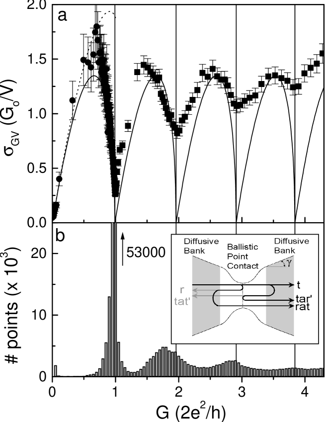
When comparing the experimental data for with our theoretical model, we need to be aware that the experimental data have been sorted according to their conductance value. A given value for can be constructed in many ways from a choice of transmission values . The experimental values for are, therefore, an average over impurity configurations and transmission values. Assuming these averages are independent, we can compare the data with various choices for the distribution of the transmissions. The dashed curve in Fig. 3a shows the behavior of for a random distribution of two ’s in the interval under the constraint , where the amplitude has been adjusted to fit the data. Alternatively, the full curve shows the behavior for a single partially open channel, i.e. in the interval there is a single channel, in there are two channels with one fully open, etc. The latter description works surprisingly well, in particular for the minimum near 1 , and for the fact that the maxima are all nearly equal.
Note that the minima in Fig. 3a are found slightly below the integer values. A reduction of the conductance with respect to the bare conductance of the contact, , results from total probability for back scattering on the same defects which give rise to the fluctuations. We can estimate the correction as the sum over incoming channels, , and their probability to return via any channel, , . The total return probability we approximate by the substitution . Thus we expect a correction term ). In Fig. 3 the vertical gray lines indicate the shift below integer values for , which is equivalent to a classical series resistance of 130 . From this value for we obtain an estimate for nm, which is consistent with the value obtained from the fluctuation amplitudes discussed below.
In our experiment we measure the second derivative with a modulation amplitude of 20 mV. This limits the path lengths to which we are sensitive to those smaller than 100 nm (). From the amplitude of the full curve in Fig. 3a we obtain an estimate of nm, assuming reasonable values for the opening angle of 30o-50o [11]. This value is consistent with our assumption that , where is the contact diameter. The estimate for is sensitive to the functional form of the factors in front of the -term in Eq. (2), which was not tested in detail. Measurements of the dependence on modulation amplitude are under way. However, the thermopower of atomic size gold contacts was recently measured [12] and has been found to be determined by the same mechanism, but it was measured on an energy scale nearly two orders of magnitude lower. It gives the same estimate of nm, consistent with the present value.
Conductance fluctuations [13] have been observed previously in ballistic contacts with diameters an order of magnitude larger compared to our contacts, and were measured as a function of both magnetic field and bias voltage [14]. In that work, the quantum suppression of the fluctuations which we report here, is not observable due to the fact that many nearly-open channels contribute to the conductance for large contacts. The model introduced by Kozub et al. [15] to describe the results of Ref. [14] contains only terms due to the interference of two diffusing trajectories, which are second order in .
The minimum observed at in Fig. 3a is very sharp, close to the full suppression of fluctuations predicted for the case of a single channel. To describe the small deviation from zero, it is sufficient to assume that there is a second channel which is weakly transmitted, , and such that . For this case it is easy to show that the value of at the minimum is proportional to the average value of . We obtain , implying that, on average only 0.5 % of the current is carried by the second channel. For the minima near 2, 3 and 4 we obtain higher values: 6, 10 and 15 %, respectively.
The well-developed structure observed in , with a dependence which closely follows the behavior of Eq. 2, demonstrates a property of the contacts which we refer to as the saturation of transmission channels: There is a strong tendency for the channels contributing to the conductance of atomic-size gold contacts to be fully transmitting, with the exception of one, which then carries the remaining fractional conductance. Fig. 3 shows that the positions of the minima in do not all coincide with those of the maxima in the histogram. This is most pronounced for the feature below . We conclude that the statistically preferred values of the histograms do not necessarily correspond with perfect transmission of the bare contact. We propose that the appearance of peaks in the histograms, such as the one at 1.75 , arises from preferred atomic configurations.
The concept of the saturation of transmission channels is consistent with recent work, which shows that, for monovalent metals, the conductance at of a single atom is carried by a single mode [16, 17, 18]. Conversely, based on the analysis of the subgap structure for superconducting aluminum by Scheer et al. [17, 19], which showed that typically three channels contribute to the conductance at , we should expect that aluminum does not show a pronounced suppression of conductance fluctuations near integer values. Indeed, preliminary measurements of on this - metal, exhibit results for that are close to a random distribution over 3 transmission channels, while the monovalent metals Ag and Cu show behavior similar to Au.
This work is part of the research program of the ”Stichting FOM”, which is financially supported by NWO. BL and JMvR acknowledge the stimulating support of L.J. de Jongh, and we thank E.Scheer and J.Caro for helpful discussions.
REFERENCES
- [1] For a review, see J.M. van Ruitenbeek, in: Mesoscopic Electron Transport, L.L. Sohn et al., eds. (Kluwer Academic Publishers, 1997)
- [2] R. Landauer, IBM J. Res. Dev. 1, 223 (1957)
- [3] J.M. Krans, et al., Nature 375, 767 (1995), M. Brandbyge, et al., Phys. Rev. B 52, 8499 (1995)
- [4] B.J. Wees, et al., Phys. Rev. Lett. 60, 848 (1988), D.A. Wharam, et al., J. Phys. C 21, L209 (1988)
- [5] N. Agraït, J.G. Rodrigo and S. Vieira, Phys. Rev. B 47, 12345 (1993); J.I. Pascual, et al., Phys. Rev. Lett 71, 1852 (1993)
- [6] G. Rubio, N. Agraït, S. Vieira, Phys. Rev. Lett. 76, 2302 (1996)
- [7] C. Sirvent, J.G. Rodrigo, N. Agraït, S. Vieira, Physica B 218, 238 (1996)
- [8] D.L. Maslov, C. Barnes and G. Kirczenow, Phys. Rev. Lett. 70, 1984 (1993)
- [9] M. Brandbyge, M.R. Sørensen, K.W. Jacobsen, Phys. Rev. B 56, 14956 (1997)
- [10] Strictly, we should consider the probability until the first return to the contact, but we estimate the correction to be of order , with the contact diameter.
- [11] C. Untiedt, et al., Phys. Rev. B 56, 2154 (1997)
- [12] B. Ludoph. J.M. van Ruitenbeek, Phys. Rev. B, submitted.
- [13] For a review of the theory, see B.Z. Spivak and A. Yu. Zyuzin, in: Mesoscopic Phenomena in Solids, B.L. Altshuler, P.A. Lee and R.A. Webb, eds. (Elsevier Science Publishers, 1991).
- [14] P.A.M. Holweg, et al., Phys. Rev. Lett. 67, 2549 (1991); P.A.M. Holweg, et al., Phys. Rev. B 48, 2479 (1993); D.C. Ralph et al., Phys. Rev. Lett. 70, 986 (1993).
- [15] V.I. Kozub, J. Caro, P.A.M. Holweg, Phys. Rev. B 50, 15126 (1994)
- [16] J.C. Cuevas, A. Levy Yeyati, A. Martín-Rodero, Phys. Rev Lett. 80, 1066 (1998)
- [17] E. Scheer et al. Nature 394, 154 (1998)
- [18] H.E. van den Brom, J.M. van Ruitenbeek, Phys. Rev. Lett. (this issue).
- [19] E. Scheer, et al., Phys. Rev Lett. 78, 3535 (1997)