Metal-Insulator Transition in a Disordered Two-dimensional Electron Gas in GaAs-AlGaAs at Zero Magnetic Field
Abstract
A metal-insulator transition in two-dimensional electron gases at is found in Ga[Al]As heterostructures, where a high density of self-assembled InAs quantum dots is incorporated just 3 nm below the heterointerface. The transition occurs at resistances around h/e2and critical carrier densities of . Effects of electron-electron interactions are expected to be rather weak in our samples, while disorder plays a crucial role.
pacs:
71.30.+h, 73.20.Jc 73.40.KpThe metal-insulator transition (MIT) is one of the central questions in the understanding of two-dimensional systems[2]. Theoretically it has been shown that a two-dimensional system without interactions is expected to behave as an insulator[3]. Recent experiments on silicon metal-oxide-semiconductor field-effect transistors (MOSFETs) with low disorder[4, 5, 6, 7] have clearly demonstrated a MIT at zero magnetic field (B=0). Meanwhile, metallic phases have also been found with holes in SiGe quantum wells[8] and holes in Ga[Al]As heterostructures[9, 10]. Scaling theory has been crucial in order to characterize the metallic and the insulating states[2, 3], even in the presence of interactions[11, 12, 13]. The resistivity has been found to scale with temperature as well as with electric field, in agreement with theoretical considerations[2],[14]. By studying both scalings, the dynamic exponent z and the correlation length exponent can be obtained independently[15]. In general, samples in which a MIT at B=0 was experimentally observed, were optimized towards low disorder and large electron-electron interaction, i.e. clean samples with large effective carrier masses and low carrier densities have been used.
Here, we report on the observation of a MIT in a disordered two-dimensional electron gas (2DEG) in a Ga[Al]As heterostructure, both as a function of temperature and electric field at B=0. The MIT in our samples is observed at a critical carrier densities of , a mobility of and at resistances of the order of . The parameters of our samples are very different to the ones used in previous work in two respects. First, the electron-electron interaction energy is comparable to the kinetic energy of the electrons. In our samples, the ratio , is only 0.9 at ( denotes the dielectric constant of GaAs, i.e. , and the effective electron mass in GaAs is where is the free electron mass) this ratio is in the samples studied in Refs. [4, 5, 6, 7, 8, 9, 10, 15]. Second, our samples are highly disordered. The Drude scattering time at is , almost 2 orders of magnitude below the scattering times in the experiments cited above. It is also two orders of magnitude below the typical dephasing time in our samples. The high disorder is generated by a layer of InAs self-assembled quantum dots (SAQD) located at the site of the electron gas. The details of the scattering centers, namely attractive InAs dots filled with electrons, are rather different from conventional disorder predominately originating from residual doping atoms. We observe the MIT at B=0 only in samples with very high dot densities of about Scaling behavior in electric field is found. Scaling in temperature is difficult to confirm because of a poorly defined fix point in the temperature dependence. Nevertheless, we can estimate z and and find values in the same range as those reported in Ref.[15]. The layout of the paper is as follows: first, we will describe the samples and the experimental setup. We proceed by discussing the temperature dependence of the MIT, followed by its electric field dependence. We speculate on a possible explanation and conclude with a summary .
The details of our samples are described in[16], but the crucial parameters are given below. A layer of InAs SAQDs is embedded in the GaAs buffer layer 3 nm from the interface that defines a 2DEG (upper right inset in Fig. 1). The substrate was not rotated during growth of the dot layer, leading of a gradient in dot density across the wafer from dots cm-2 up to dots cm-2. From TEM studies and transport measurements, the dot density is known within a factor of 2 for each part of the wafer. A -doping (n-type with Si) layer within the 30 nm from the interface provides the carriers for the 2DEG. The MIT at B=0 was observed for the sample with the highest density of dots, namely sample 7 from[16]. To ensure a homogeneous dot density, the sample size was kept sufficiently small. The width of the Hall geometries is , while the voltage probes used to measure are separated by Gate electrodes are used to change the carrier density. The samples are immersed in the mixing chamber of a dilution refrigerator with a base temperature of . Resistivites were measured at low frequencies () in a four-probe configuration at a current level of 1nA. For the electric field scaling, the DC bias current was swept and the voltage drop was measured.
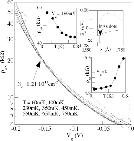
In the following, we focus on the sample with the high dot density. Fig. 1 shows traces
as a function of gate voltage at zero
magnetic field for temperatures between and .
The traces cross each other at a
resistivity slightly below and at a gate voltage of ,
corresponding to . At lower densities (), the sample
behaves insulating, i.e. the resistivity
increases with decreasing
temperature (upper left inset in Fig. 1). At densities above the
fix point, the resistivity
drops with decreasing T, indicating a metallic character (lower right
inset in Fig. 1). The T dependence
saturates around . The saturation of in the metallic phase
at low T is not due to current heating, since the same traces do not saturate in the insulating
regime. Rather, the T dependence
can be fitted by, as observed in[10] and predicted
theoretically from two different
models[14],[17]. Since the
fix point of the MIT is poorly defined, scaling according to
, and denotes the scaling function
in T) is difficult to confirm, although from scaling attempts (not shown)
we can estimate .
Samples with lower dot density from the same wafer did not display a
MIT at B=0. They displayed
insulating behavior for all available carrier densities, with the
temperature dependence of the
resistance becoming very small for high carrier densities.
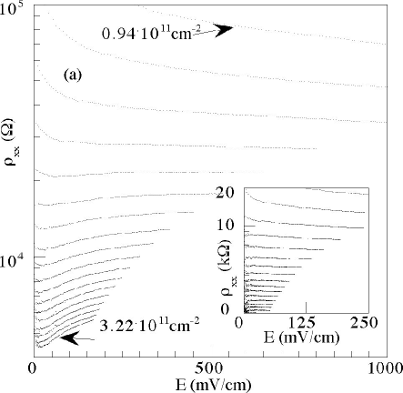
In Fig. 2a, as a function of the electric
field is shown for various electron densities. Again, a MIT is
clearly visible, similar to the results
in[15]. and at the
transition are the same as those
found in the T dependence. The inset in Fig.2a shows the result of
a similar experiment on a sample
with lower dot density of about dots No metallic
phase could be found.
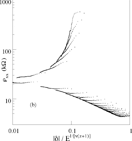
Fig. 2b shows the result of scaling according to . For the best visual
collapse of the curves onto one trace, we find
The scaled curves show a stronger asymmetry
than those obtained from
scaling in Si MOSFETs[15], but similar to the asymmetry observed
for hole systems in GaAs[9]. This asymmetry, however, is not surprising, since it is a
measure for the nonlinearity of the
function around the critical point[12]. Each individual curve
contains several points that
deviate from the scaled function. These points correspond to the low
electric field range
Fig.2a). At these small electric fields, the
resistivity increases slightly and may indicate are-entrant behavior
into an insulating phase. Due to the small
sample size, however, the experimental error is larger at small electric
fields. This low-electric field regime at high electron densities
needs further study and is not discussed here.
Combining the results for the scaling exponent obtained from
electric field scaling and the
estimated value for the temperature scaling as described above, we
find and
Due to the large error bars, we do not attempt to
give a detailed interpretation.
However, these numbers are in agreement with the values reported
in[15] and
in agreement with theoretical
considerations, i.e. for an interacting system [2] and
from percolation theory[14].
At present, we do not
have a full understanding of the
existence of a metallic phase in our samples. It is clear, however,
that a high density of SAQDs is needed for its formation. In the following, we speculate on possible
explanations on what the metallic phase consists of and discuss
magnetoresistance measurements. Within a two-phase model[14],
a gaseous phase can coexist with a liquid phase
which can undergo a percolation
threshold that defines the transition point from a metal to an
insulator. In our sample, the
liquid phase could be formed by the disordered electron gas, while the
localized gas phase may consist of minibands or quasi-bound states that
emerge from the SAQDs.
The conduction band is lowered in regions were the InAs dots form. For the first electron in the empty conduction band this leads to an attractive potential well. As more electrons populate the conduction band they first fill the InAs dots and then build up a Fermi sea. For the mobile electrons in the GaAs conduction band the filled InAs quantum dots now represent repulsive scattering centers. The potential landscape can be viewed as a random antidot lattice with possible short-range ordering. From our previous experiments we know that each dot is populated by about two electrons[16]. The depth of the InAs wells (100-200 meV) is about an order of magnitude larger than the Fermi energy (). However, the presence of the InAs dots can lead to quasi-bound states in the continuum of the dots close to the range of the Fermi energy. Since the InAs dots are rather homogeneous in size (the dot diameter varies by only about 7% [18] ) and energetic structure[19], these quasi-bound states are expected to be rather narrow as well. In principle, mobile electrons can scatter into and out of such quasi-bound states which leads to a decreased conductivity compared to the 2DEGs without SAQDs. The states that are available for the electrons to scatter into are within an energy window of . In this picture, a lower electron temperature would lead to a smaller number of available states and thus to an increasing conductivity with decreasing temperature, as in a metallic state. A similar situation is considered in[20], where the structure of 2D electronic states in a strong magnetic field in the presence of a large number of resonant scatterers is calculated. So far, in transport experiments on electron gases with InAs SAQDs nearby[21], such states have not been observed; however, note that higher dot densities than in these experiments are needed. In case a short-range order between the SAQDs exists, a local bandstructure may arise leading to an increased effective mass. This could give rise to an enhancement of the Coulomb interaction.
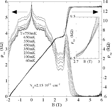
Clearly, the electrons form a quantum Hall liquid at sufficiently high magnetic fields in all our samples. The longitudinal magnetoresistivity as well as the Hall resistivity for the sample with the high dot density shown in Fig.3. At , the sample is in a metallic state. Above , the sample is in a quantum Hall state with filling factor 2 (i.e. 2 Landau levels are occupied). In , a fix point occurs at a magnetic field of as shown in the inset. Such magnetic field driven insulator-to-quantum Hall-liquid transitions have been experimentally observed in other disordered 2DEGs (for a review, see [2] and references therein). In our system, a fix point occurs in , while increases for increasing temperature over the entire magnetic field range. A scaling analysis around the fix point in reveals a scaling exponent of , in good agreement with exponents found in standard spin-degenerate quantum Hall systems [22]. These transitions can also be observed in samples with lower density of InAs dots, where a fix point is also observed in . This is in tune with the fact that these samples always display insulating behavior at and crossing points at finite magnetic fields are therefore possible.
In our high dot density sample, the metallic phase is not destroyed by the application of parallel magnetic fields. Under parallel magnetic fields up to , the electric field scaling of the metallic phase remains unchanged.
To conclude, our experimental data clearly indicate the occurrence of a metal-insulator transition at zero magnetic field in a disordered two-dimensional electron gas in a Ga[Al]As heterostructure. Scaling theory has been applied to both the temperature dependence and the electric field dependence. While electric field scaling works well, temperature scaling is poor since the fix point in temperature is poorly defined. We have estimated the scaling exponents for our sample to and , in agreement with the current framework of scaling theory and percolation theory. We speculate that it is the special kind of disorder potential in our samples that possibly modifies the ratio between the electron-electron interaction energy and the kinetic energy and thus drives this transition. In that sense the metal-insulator transition in two-dimensional systems remains a research topic that is far from being understood and requires more experimental as well as theoretical work.
We are grateful to T. Ihn, C. F. Zhang, T. M. Rice, and S. Ulloa for helpful discussions. This work was supported by the Schweizerische Nationalfonds and by QUEST. E. R. acknowledges financial support from Fundação de Amparo à Pesquisa do Estado de São Paulo.
REFERENCES
- [1] Present address: Instituto de Física “Gleb Wataghin”, Universidade Estadual de Campinas, 13081-970 Campinas, SP, Brazil.
- [2] For a recent review, see S. L. Sondhi, S. M. Girvin, J. P. Carini, and D. Sahar, Rev. Mod. Phys. 69, 315 (1997)
- [3] E. Abrahams, P. W. Anderson, D. C. Licciardello, and T. V. Ramakrishnan, Phys. Rev. Lett. 42, 673 (1979)
- [4] S. V. Kravchenko, G. V. Kravchenko, J. E. Furneaux, V. M. Pudalov, and M. D’Iorio, Phys. Rev. B 50, 8039 (1994)
- [5] S. V. Kravchenko, W. E. Mason, G. E. Bowker, J. E. Furneaux, V. M. Pudalov, and M. D’Iorio, Phys. Rev. B 51, 7038 (1995)
- [6] D. Simonian, S. V. Kravchenko, M. P. Sarachik, and V. M. Pudalov, Phys. Rev. Lett. 79, 2304 (1997)
- [7] D. Popovic, A. B. Fowler, and S. Washburn, Phys. Rev. Lett. 79, 1543 (1997)
- [8] J. Lam, M. D’Iorio, D. Brown, and H. Lafontaine, Phys. Rev. B 56, R12741 (1997)
- [9] M. Y. Simmons, A. R. Hamilton, M. Pepper, E. H. Linfield, P. D. Rose, D. A. Ritchie, A. K. Savchenko, and T. G. Griffiths, Phys. Rev. Lett. 80, 1292 (1998)
- [10] Y. Hanein, U. Meirav, D. Sahar, C. C. Li, D. C. Tsui, and H. Shtrikman, Phys. Rev. Lett. 80, 1288 (1998)
- [11] A. M. Finkel’stein, Zh. Eksp. Teor. Fiz. 84, 168 (1983) [Sov. Phys. JETP 57, 97 (1983)]
- [12] V. Dobrosavljevic, E. Abrahams, E. Miranda, and S. Chakravarty, Phys. Rev. Lett. 79, 455 (1997)
- [13] C. Castellani, C. Di Castro, and P. A. Lee, Phys. Rev. B 57, R9381 (1998)
- [14] Song He and X.C. Xie, Phys. Rev. Lett. 80, 3324 (1998)
- [15] S. V. Kravchenko, D. Simonian, M. P. Sarachik, W. Mason, and J. E. Furneaux, Phys. Rev. Lett. 77, 4938 (1996)
- [16] E. Ribeiro, E. Müller, T. Heinzel, H. Auderset, K. Ensslin, G. Medeiros-Ribeiro, and P. M. Petroff, Phys. Rev. B 58, 1506 (1998)
- [17] V. M. Pudalov, JETP Lett. 66, 175 (1997)
- [18] D. Leonhard, M. Krishnamurthy, C. M. Reaves, S. P. Denbaars, and P. M. Petroff, Appl. Phys. Lett. 63, 3203 (1993)
- [19] H. Drexler, D. Leonhard, W. Hansen, J. P. Kotthaus, and P. M. Petroff, Phys. Rev. Lett. 73, 2252 (1994)
- [20] T. V. Shahbazyan and S. E. Ulloa, Phys. Rev. Lett. 79, 3478 (1997)
- [21] H. Sakaki, G. Yusa, T. Someya, Y. Ohno, T. Noda, H. Akiyama, Y. Kadoya, and H. Noge, Appl. Phys. Lett. 67, 3444 (1995); G. Yusa and H. Sakaki, Appl. Phys. Lett. 70, 345 (1997); N. Horiguchi, T. Futatsugi, Y. Nakata, and N. Yokoyama, Appl. Phys. Lett. 70, 2294 (1997)
- [22] H. P. Wei, S.W. Hwang, D.C. Tsui, and A. A. M. Pruisken, Surf. Sci. 229, 34 (1990)