Skipping orbits and enhanced resistivity
in large-diameter
InAs/GaSb antidot lattices
pacs:
73.50.Jt, 05.45+b, 73.20.DxPeriodically modulated two-dimensional electron gases (2DEGs) offer the possibility to study electron motion in artificially tailored periodic potentials.[2] If the modulation potential is strong enough to deplete parts of the 2DEG around the potential maxima the system is called an antidot (AD) array. Antidot lattices are model systems to study both the classical chaotic motion of electrons in the potential landscape as well as resulting bandstructure effects.[2] Investigations so far have essentially focused on the low field regime where the low-temperature magnetoresistance reflects peaks whenever the classical cyclotron diameter fits around a (geometry-dependent) specific number of antidots.[3] The last maximum appears in the resistivity when is equal to the period of the array. Here we focus on novel structure appearing at slightly higher fields corresponding to -values where holds. While antidot lattices are usually based on GaAs/AlGaAs heterojunctions, we used here the material system InAs/GaSb to fabricate antidot arrays. Due to the pinning of the Fermi energy within the conduction band at open surfaces of InAs,[4] depletion regions around the antidots should be significantly smaller than in GaAs based systems. This should allow, due to the resulting steep potential posts, to fabricate very short period antidot arrays or, as it is the case here, the fabrication of large antidots with small constrictions between neighboring antidots.
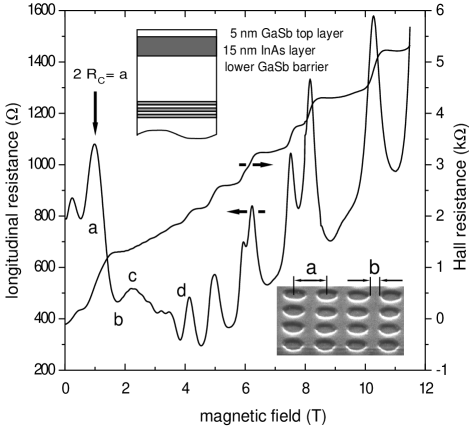
Our samples are fabricated from InAs/GaSb heterostructures grown on undoped GaAs substrates by molecular beam epitaxy. The epitaxial layers on the substrate consist of a m AlGaSb layer, a m thick GaSb buffer followed by a ten period AlSb/GaSb superlattice, the GaSb barrier of thickness, the InAs quantum well and a GaSb top layer (see upper inset in Fig. 1). While the heterostructure is nominally undoped, the carrier concentration can be adjusted by the top layer thickness.[5, 6, 7] Typical values of in our unpatterned samples were about . Hall-bars were defined by standard photolithography and wet chemical etching. [8] It turned out that the alkaline photoresist developer attacks the GaSb-layer and decreases the carrier mobility from about to about . An annealing step at C in a continuous flow of forming gas restored the mobility to about . This corresponds to a mean free path of m which is much larger than the lattice period nm, thus making commensurability features observable. Since InAs does not form a Schottky barrier to metals, it was not necessary to use alloyed contacts. Instead of gold, which proved to react with GaSb in the final annealing step, we used evaporated indium contacts. The antidots were defined with electron beam lithography and etched with the solution described above. A scanning electron micrograph of the samples showed the antidots to be uniform in size and shape with an AD diameter of .
The four-point magnetotransport measurements were carried out at temperatures ranging from K to K using standard lock-in techniques. Utilising the negative persistent photo-conductivity of InAs quantum wells,[9] the carrier density could be varied by illuminating the sample with a red LED. The magnetoresistance and Hall resistance traces at a carrier density of and a temperature of K are shown in Fig. 1. At low fields two commensurability peaks in the magnetoresistance curve can be observed. The peak at about T belongs to trajectories going around one antidot, the other one at T corresponds to a deformed cyclotron orbit around four antidots. In the simplest model, the enhanced resistivity at these field values can be ascribed to electrons pinned on commensurate cyclotron orbits, which cannot carry current.[3, 11] At fields above T strong Shubnikov-de Haas (SdH) oscillations appear and from T spin-splitting of the Landau levels is resolved. By comparison to an unpatterned reference sample, we can conclude that the quality of the 2DEG was not seriously affected by the patterning process. In the region between T and T we find a new broad peak structure whose origin will be discussed below. In earlier work, a corresponding shoulder was ascribed to etch-induced defects.[10] For a sample with triangular antidots, a high-field shoulder at was explained by electrons being reflected on the straight antidot edges.[12]
Figure 2 shows the dependence of the magnetoresistance traces on the carrier density (changed by illumination) and temperature (inset). The novel peak structure shifts similar to the main commensurability maximum at . This suggests, together with the weak temperature dependence of the peaks (see lower inset of Fig. 2), a classical origin of the phenomenon. Associating the magnetic field value at which the broad maxima start to appear (marked by arrows) with the matching condition we find a value of nm. This value corresponds to the distance between neighboring antidots in our device. This finding is consistent with the assumption that the broad maximum is associated with rosetta shaped orbits skipping around one antidot, as we will show below.
Superimposed on the classical peak we find -periodic quantum oscillations. While the periodicity of these oscillations is similar to the period of the SdH-oscillations at higher magnetic field, there is a distinct transition between the high-field oscillations and the ones superimposed upon the classical maximum. This can be seen in the upper inset of Fig. 2 where the filling factor is plotted versus . At around 4 T there is a pronounced kink in the otherwise linear slope which is observed at the transition between the classical peak regime and the quantum mechanical regime in which Shubnikov-de Haas oscillations dominate. Compared to the Shubnikov-de Haas oscillations the amplitude of oscillations superimposed upon the classical peak structure is strongly suppressed. We speculate that the weak -periodic oscillations in the low field regime stem from quantization of the skipping orbits. The quantum oscillations are suppressed at temperatures above a few Kelvin (see lower inset of Fig. 2) while the classical features survive up to temperatures of K where they are blurred as the GaSb substrate becomes conducting.

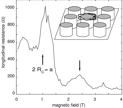
In order to clarify the origin of the classical maximum between T and T we carried out numerical calculations following recent work.[11] We evaluated the Kubo formula [13]
to calculate the conductivity tensor where the indices and stand for the - and -direction. The trajectories and the resulting velocities and were calculated numerically assuming a hard wall potential. The brackets denote the average over phase space. Previously only chaotic trajectories were considered in the evaluation of the Kubo formula.[11] Since the features we are interested in appear at relatively high magnetic field values, most of the phase space is occupied by regular non-chaotic trajectories. Therefore we included both regular and chaotic trajectories in our calculations.By inverting the conductivity tensor we obtain the experimentally determined diagonal resitivity . The results of a simulation using the simple model with perfectly hard walls are shown in Fig. 3. The calculated traces are remarkably close to the experimental results: the additional structure between 1.5 and 3.5 T was nicely reproduced.[14]
To obtain information about the types of trajectories involved in the observed magnetoresistance anomalies we analysed the Poincaré surfaces of section at different magnetic field values. This is done by injecting electrons at (between two antidots; see left hand side of the lower inset of Fig. 4) with velocity into the lattice and recording the and values of the injected electrons intersecting the line . To take into account possible soft wall effects we assumed here an antidot potential of the form
with . The trajectories and velocities of the injected electrons were obtained by solving the classical equations of motion numerically at several magnetic fields (indicated with letters a to d in Figs. 1 and 4).

At about T (letter a), the commensurability condition is satisfied, and the Poincaré surface of section exhibits a stable island in Fig. 4a belonging to cyclotron orbits around one antidot. This leads to the fundamental commensurability peak in . The minimum in the magnetoresistance at T (letter b) is due to the fact that the large antidots leave no room for stable trajectories. This minimum is not found in antidot lattices with smaller AD diameters.If the magnetic field gets higher, the Poincaré surface of section c shows that a large fraction of phase space is occupied by periodic and quasi-periodic trajectories. These are rosetta shaped orbits, which encircle one antidot and remain stationary even if an electric field is applied in the simulation, giving rise to a maximum in the magnetoresistance at T. The situation is quite similar to pinned orbits, which are responsible for the commensurability peak at . The high field behaviour (letter d, T) of the classical structure is governed by the formation of unstable rosetta orbits. Instead of being composed more or less of semicircles, the small cyclotron diameter at high fields permits orbits which resemble circles revolving around one antidot. These orbits tend to drift perpendicular to an electric field, thus reducing , even though the stable orbits still occupy a large volume in phase space.
When the magnetic field exceeds T, the amplitude of the SdH-oscillations increases drastically. At lower fields the cyclotron diameter exceeds the width of the constriction between adjacent antidots. Therefore, electrons can move easily from one edge of the sample to the other by hopping from AD to AD. As soon as the cyclotron diameter becomes smaller, this backscattering process is no longer possible and the SdH-oscillations become much more pronounced. From the magnetic field position of this point we determine this critical cyclotron diameter to be . If we assume a very steep antidot potential, this leads to an antidot diameter of which is a little larger than the lithographic diameter of . Since on InAs surfaces the Fermi level is pinned in the conduction band,[4] one would not expect a depleted region enlarging the antidots. However, the exact pinning position of the Fermi level depends on the detailed conditions of the etch-exposed surfaces and may well be different from the bulk Fermi level in the 2DEG.[15] Consequently, the enhancement of the antidot diameter can be due to a softer potential.
In summary, we fabricated and measured antidot arrays on InAs/GaSb with large AD diameters. We find a broad maximum in the magnetoresistance at intermediate magnetic fields characterized by as lower and as upper edge, which we show to be of classical origin. The trajectories responsible for this maximum are identified to be rosetta orbits around single ADs. We also observe weak quantum oscillations on this maximum, which we speculate to originate from quantized rosetta orbits. Finally, we estimate the effective diameter of the ADs and find that it is comparable with the lithographic diameter.
We would like to thank D. Heisenberg for helpful discussions. The authors acknowledge the financial support of the German Bundesministerium für Bildung und Forschung under Contract No. 01 BM 622/5.
REFERENCES
-
[1]
Electronic address:
jonathan.eroms@physik.uni-regensburg.de - [2] Mesoscopic Physics and Electronics, edited by T. Ando, Y. Arakawa, K. Furuya, S. Komiyama, and H. Nakashima (Springer-Verlag, Berlin, 1998)
- [3] D. Weiss, M. L. Roukes, P. Grambow, K. von Klitzing, G. Weimann, Phys. Rev. Lett. 66, 2790 (1991).
- [4] L. Ö. Olsson, C. B. M. Andersson, M. C. Håkansson, J. Kanski, L. Ilver, U. O. Karlsson, Phys. Rev. Lett. 76, 3626 (1996).
- [5] M. Altarelli, J. C. Maan, L. L. Chang, L. Esaki, Phys. Rev. B 35, 9867 (1987).
- [6] C. Nguyen, B. Brar, H. Kroemer, J. H. English, Appl. Phys. Lett. 60, 1854 (1992).
- [7] C. Nguyen, B. Brar, H. Kroemer, J. Vac. Sci. Technol. B 11, 1706 (1993).
- [8]
- [9] F.-C. Wang, W. E. Zhang, C. H. Yang, M. J. Yang, B. R. Bennett, Appl. Phys. Lett. 69, 1417 (1996).
- [10] D. Többen, M. Holzmann, S. Kühn, H. Lorenz, G. Abstreiter, J. P. Kotthaus, F. Schäffler, Phys. Rev. B 50, 8853 (1994).
- [11] R. Fleischmann, T. Geisel, R. Ketzmerick, Phys. Rev. Lett. 68, 1367 (1992).
- [12] A. Lorke, S. Wimmer, B. Jager, J.P. Kotthaus, Proc. EP2DS-12 105 (1997), to appear in Physica B.
- [13] R. Kubo, J. Phys. Soc. 12, 570 (1957).
- [14] The calculation shows a double peak structure (with maxima at 2.4 and 3.3T). This double peak structure is not unlike the one observed in experiment, see e.g. the bottom trace in Fig.2. While the structure can be ascribed to rosetta orbits we have no clear picture yet about the origin of the splitting.
- [15] B. J. van Wees, G. I. Meijer, J. J. Kuipers, T. M. Klapwijk, W. van de Graaf, G. Borghs, Phys. Rev. B 51, 7973 (1995).