Gain Dependence of the Noise in the Single Electron Transistor
Abstract
An extensive investigation of low frequency noise in single electron transistors as a function of gain is presented. Comparing the output noise with gain for a large number of bias points, it is found that the noise is dominated by external charge noise. For low gains we find an additional noise contribution which is compared to a model including resistance fluctuations. We conclude that this excess noise is not only due to resistance fluctuations. For one sample, we find a record low minimum charge noise of in the superconducting state and in the normal state at a frequency of 4.4 kHz.
1 Introduction
With the introduction of the Single Electron Transistor (SET) one decade ago, it became possible to directly measure changes in charge quantities below that of an electron [1, 2]. Based on the Coulomb blockade, the device has been shown to be the most sensitive electrometer existing today. The sensitivity of the SET is predicted to be limited by the shot noise [3] generated when electrons tunnel across the tunnel barriers [4]. Shot noise was observed in a two junction structure (without gate) [5]. In most experiments involving SETs, the noise for low frequencies has been dominated by the device itself, whereas external sources set the noise limit for frequencies above the kHz regime.
Several experimental studies of low frequency noise of various SET configurations have been performed [6]-[18]. Below 1 kHz, noise is observed in all SETs regardless of mode of operation [7]-[16]. The input equivalent charge noise at 10 Hz in all these experiments is of the order of to , with recently reported as the lowest figure [17]. Deviations from an spectrum are often observed, usually in combination with telegraph noise [7, 15]. The source of the latter is believed to be random excitations of a single charge trap. Theoretically, the random trapping process of a single trap shows a Debye-Lorentzian power spectrum [19] which is also observed experimentally [8, 12, 13]. It has been shown that an ensemble of traps produces a noise spectrum, see e.g. [22].
There are at least three possible locations of these fluctuators: the tunnel junction dielectric, the substrate on which the device is fabricated, and the oxide layer covering the device. The role of the substrate has been examined in at least two sets of experiments [12, 18]. Those experiments did not show a strong dependence of the noise on the substrate material. The barrier dielectric has been proposed as the location of charge traps [8, 9, 15, 17]. The role of the surface oxide of the island has not yet been investigated.
Several groups have found that the noise at the output of the SET varies with the gain of the SET and that the maximum noise is found at the bias point with maximum gain [8]-[11]. This indicates that the noise source acts at the input of the device, i.e. as an external fluctuating charge. However, a detailed comparison of the noise to the gain has not been done.
In this Letter, we report the low frequency current noise of one
SET and one SET and make a detailed comparison with the
gain. (Hereafter, we
will refer to the two SETs as the Al SET and the Nb SET). For the Al SET,
we find that the
noise follows the gain in such a manner that the SET is dominated by input
noise for almost all values of bias and gate voltage. For the Nb SET
however, we find a contribution from other sources when analysing the noise
in the points where the gain is low.
2 Experimental Techniques
The samples were fabricated on oxidised Si substrates using electron beam lithography and the standard double-angle evaporation technique [20].
The resistance of the Al SET directly after fabrication was k, which after a storage for six months, had increased to k. The Nb SET had a resistance of k.
We used a symmetric, current sensitive amplifier which voltage biased the SET [10]. To optimize the preamplifier noise performance low noise operational amplifiers with low noise were used. Furthermore, the bias (feedback) resistors were chosen to M to lower the amplifier noise floor at low frequencies.
The SETs were attached to the mixing chamber of a dilution refrigerator which was cooled to a temperature below 30 mK. All measurement leads were filtered with 0.5 m Thermocoax [21] followed by capacitors to ground. The total line capacitance was =1 nF.
Evaluating the frequency performance, we found a gain bandwidth of the SET setup of 7.5 kHz while the noise bandwidth was about 300 Hz (without any SET connected). Both these figures were set by the line capacitance and the preamplifier [10].
The noise spectra were recorded by a HP 35665A Dynamic Signal Analyzer, which performs real-time FFT analysis of the input signal. The frequency range from 1 to Hz was divided into four subranges to increase the resolution. The time to acquire all noise data for one bias point was 5 min.
3 Results and Discussion
Two samples were tested. The current-voltage characteristics for the Al SET are shown in Fig. 1a, both for the normal and the superconducting state. A total island capacitance of fF was deduced from the IV-curves. The Nb SET had fF. The output impedance, , was calculated from the curves. In the superconducting state was always above k while in the normal state, was on the order of, or above for both SETs. The gate coupling capacitances were aF and aF for the Al and the Nb SETs, respectively.
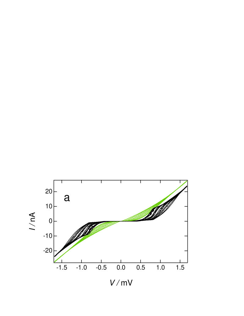
Due to its low resistance, the AL SET had a very high maximum gain of nA/e and nA/e in the normal and superconducting states, respectively. The Nb SET had nA/e and nA/e in the normal and superconducting states. The gain increase in the superconducting state is in accordance with earlier observations [14, 15].
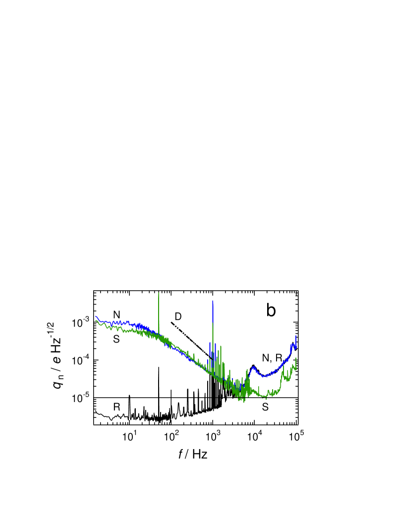
Noise spectra for the normal and superconducting states of the Al SET are shown in Fig. 1b. Each spectrum has been referred to the input of the SET by dividing by the frequency dependent gain. The spectra N and S were measured at the bias points which gave maximum gain. For reference, a spectrum with no SET connected, R, is also shown and is divided by the same gain as in the normal state to obtain the input referred noise floor set by the amplifier. Minimum charge noises of and at a frequency of 4.4 kHz was found in the superconducting and normal states, respectively. The limit is set by the preamplifier and mechanical resonances within the cryostat. These numbers are, to our knowledge, the lowest values reported for any SET. The noise at 10 Hz was and for the superconducting and normal states, respectively. A cross-over from input dominated to output dominated noise can be seen as the frequency increases. Below 1 kHz, the input referred noise is actually the same in both normal and superconducting states, indicating that the noise source acts as an apparent charge noise, and thus is independent of gain. Above 1 kHz the noise is dominated by sources acting at the output of the SET. When referred to the input, this noise appears as a lower equivalent charge noise in the superconducting state as compared to the normal state, due to the higher gain in the superconducting state.
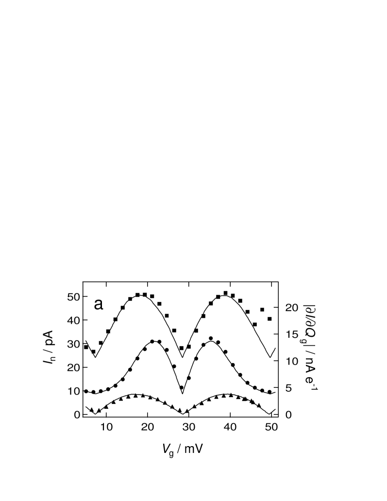
We now turn our attention to the noise below 1 kHz. To determine the origin of the noise, we measured noise for 130 bias and gate voltages and compared it with the measured gain of the SET. All points were taken in the normal state at a temperature of mK. The output current noise and the gain versus gate bias for the Al SET are shown in fig. 2a for three bias voltages. To reduce fluctuations, the noise was integrated in the band 51 to 99 Hz. By using the gate charge offset as the only fitting parameter, we were able to get an excellent fit of the noise to the gain. This result clearly shows that the noise source acts at the input of the SET. It is supposedly due to the motion of background charges somewhere in the vicinity of the SET-transistor. For the points of large gain we can deduce the spectral density of the charge fluctuations, . The Nb SET also showed a gain dependent output noise, but with more spread in the data.
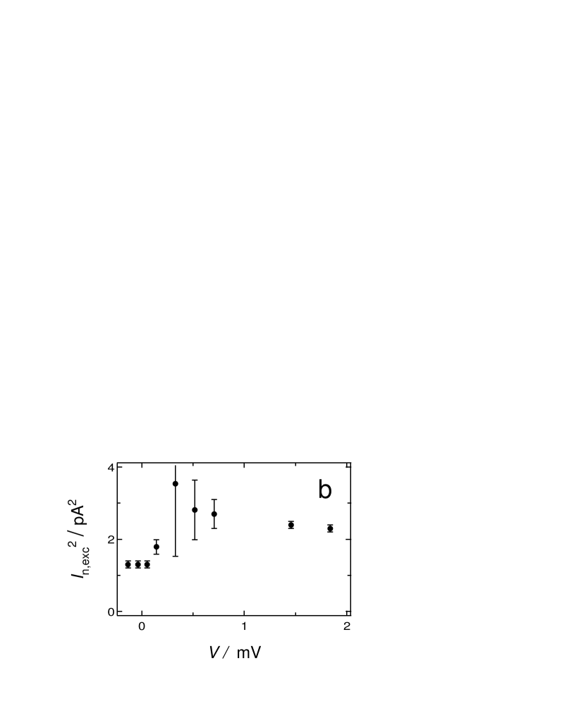
In bias points with low gain (high bias or ) it is possible to examine other noise contributions. For each , we define the excess noise current as
| (1) |
where , and , are the measured current power spectra and gains for each at minimum and maximum gain respectively. This quantity is zero when the gain dependent noise is the only contribution.
The Al SET showed excess noise only at the highest bias point, , whereas the Nb SET showed excess noise at several bias points. To gain more knowledge about the noise contributions we next discuss the different components of the measured noise.
Except for charge noise sources somewhere in the vicinity of the transistor, current noise can also be induced by fluctuations in the tunnel barrier resistance. As we will see, these two contributions can generally not be separated. There are also contributions from shot noise and amplifier noise. In our case, the amplifier noise is dominated by the thermal noise of the two feedback resistors and the noise generated by the input equivalent voltage noise, , of the amplifier. For low temperatures, the shot noise is given by , where , with for strongly correlated tunneling and for uncorrelated tunneling [4]. The total measured current noise in the system can be modelled by
| (2) |
where is the temperature of the feedback resistors and is the combined spectral density due to charge and resistance fluctuations. The first two terms represent amplifier noise and are frequency independent in the range of interest (51-99 Hz). The third term is the shot noise of the SET which also is independent of frequency. These terms are of order for the worst case with lowest and high I. Thus, the sum of these three terms varies only slightly between and for all bias points. To evaluate the last term let us start with a model in which the only fluctuating parameter is the background charge . Assuming small variations we can write
| (3) |
If only the first (linear) term is taken into account, then obviously where and are the background charge spectral densityand the charge induced current spectral density. As seen in fig. 2a we are close to this situation in the experiment.
Close to the operation points for which , the contribution from the quadratic term in eq. (3) becomes important. Assuming Gaussian noise we get
| (4) |
where . For the SETs, we find . This is smaller than the two orders of magnitude of dynamic range we have in the noise measurement and we can thus neglect the second term.
Now let us consider a different model in which does not fluctuate, and the only fluctuating parameter is the tunnel resistance of the first junction. (The fluctuations of the tunnel junction resistance have been extensively studied in large area junctions, see e.g., Refs. [22].) For simplicity let us limit ourselves to the linear term of the series expansion, so that , where can be calculated [4]. Note that is asymmetric around as a function of for [23], while it becomes independent of and proportional to for large . Furthermore, the fluctuations of can in principle change with , , and (however, a strong dependence on and is unlikely).
On the other hand the current noise which is due to fluctuations decreases for sufficiently large because of the decrease in and is symmetric around for a symmetric SET-transistor. Therefore, the bias dependence and this asymmetry could be used to distinguish the charge fluctuations from the resistance fluctuations.
In general, the noise can also be caused by simultaneous fluctuations of , , and . If they are uncorrelated, the corresponding current spectral densities should simply add. However, fluctuators inside the tunnel barrier, which have been suggested as the source of the noise by several authors [8, 9, 15, 17], can be responsible for both resistance and charge fluctuations. Then, these contributions are correlated and we arrive at the following expression
| (5) |
is the dimensionless correlation coefficient between and fluctuations, .
The first term in eq. (5) describes the dominating gain dependent noise, while the other terms contribute to the excess noise. We can now compare the bias dependence of the excess noise measured in the Nb SET to that of eq. (5). From the integrated noise spectra we calculate the measured excess current noise , according to eq. (1) and plot it versus in fig.2b. seems to increase with bias voltage, but there is no quadratic dependence which would be expected from eq. (5). It thus seems likely that the excess noise is not due to resistance fluctuations, but has a different origin. One possible explanation is that the increasing current heats the SET and generates more noise. Furthermore, at the highest bias point we can set an upper level for the resistance fluctuation in the frequency range from 51-99 Hz, . Assuming a symmetric SET ( and ) we get for the Nb SET and for the Al SET.
In conclusion we have measured the low frequency noise of two single electron transistors. In both transistors, the noise at the output closely followed the gain. This shows that low frequency noise in the SET is mainly due to external charge noise. When the gain was low, we observed an excess noise in the Nb SET for all bias voltages and in the Al SET for the highest bias voltage. From the bias dependence of the excess noise in the Nb SET we conclude that the main source of the excess noise is not resistance fluctuations. We also set an upper limit for the resistance fluctuations. The Al SET had a very high gain and showed a minimum charge noise and in the superconducting and normal state, respectively.
4 Acknowledgements
We gratefully acknowledge discussions with K.K. Likharev and A.B. Zorin. The samples were fabricated in the Swedish Nanometer Laboratory. This work was sponsored by the Swedish SSF and NFR, by the ESPRIT project CHARGE and by the Japanese NEDO.
References
- [1] Likharev K. K., IEEE Trans. Mag. 23, 1142 (1987)
- [2] Fulton T. A. and Dolan G. J., Phys. Rev. Lett. 59, 109 (1987)
- [3] Schottky W., Ann. Phys. 57, 541 (1918)
- [4] Korotkov A. N., Averin D. V., Likharev K. K. and Vasenko S. A. in Single Electron Tunneling and Mesoscopic Devices, edited by H. Koch (Springer, New York, 1992) p. 45
- [5] Birk H., de Jong M. J. M. and Schoenenberger C., Phys. Rev. Lett. 20, 1610 (1995)
- [6] Kuzmin L. S., Delsing P., Claeson T. and Likharev K. K., Phys. Rev. Lett. 62, 2539 (1989)
- [7] Zimmerli G., Eiles T. M., Kautz R L. and Martinis J.M., Appl. Phys. Lett. 61, 237 (1992)
- [8] Verbrugh S. M., Benhamadi M. L., Visscher E. H. and Mooij J. E., J. Appl. Phys. 78 (1995), 2830
- [9] Zorin A. B., Ahlers F.-J. , Niemeyer J., Weimann T., Wolf H., Krupenin V. A. and Lotkhov S. V., Phys. Rev. B 53, 13682 (1996)
- [10] Starmark B., Delsing P., Haviland D. B. and Claeson T., in Ext. Abstr. 6th International Superconductive Electronics Conference, pp. 391-393, (Berlin, 1997)
- [11] Tavkhelidze A. N. and Mygind J., J. Appl. Phys. 83, 310 (1998)
- [12] Bouchiat V., Ph.D. Thesis, Paris 6 (1997), pp. 202
- [13] Zimmerman N. M., Cobb J. L. and Clark A. F., Phys. Rev. B 56, 7675 (1997)
- [14] Hergenrother J. M., Tuominen M. T., Tighe T. S. and Tinkham M., IEEE Trans. Appl. Supercond. 3, 1980 (1993)
- [15] Song D., Amar A., Lobb C. J. and Wellstood F. C., IEEE Trans. Appl. Supercond. 5, 3085 (1995)
- [16] Zorin A. B., Pashkin Y. A., Krupenin V. A. and Scherer H., in Ext. Abstr. 6th International Superconductive Electronics Conference, pp. 394-396, (Berlin, 1997)
- [17] Krupenin V. A., Presnov D. E., Scherer H., Zorin A. B. and Niemeyer J., cond-mat/9804197.
- [18] Niemeyer J. et. al., private communication
- [19] Machlup S., J. Appl. Phys. 25, 341 (1954)
- [20] Dolan G. J., Appl. Phys. Lett. 31, 337 (1977)
- [21] Zorin A. B., Rev. Sci. Instrum. 66, 4296 (1995)
- [22] Rogers C. T. and Buhrman R. A., Phys. Rev. Lett. 53, 1272 (1984); Phys. Rev. Lett. 55, 859 (1985) Savo B., Wellstood F. C., and Clarke J., Appl. Phys. Lett. 50, 1757 (1987).
- [23] The noise is larger when the current is determined by the fluctuating junction resistance to a greater extent than by the other junction.