Observation of Strong Coulomb Blockade in Resistively Isolated Tunnel Junctions
Abstract
We report measurements of the Coulomb-blockade current in resistively isolated ( tunnel junctions for the temperature range mK mK where the charging energy is much greater than the thermal energy. A zero-bias resistance of up to (the tunnel resistance of the bare junction) is obtained. For the - curves for a given scale as a function of , with over a range of The data agree well with numerical calculations of the tunneling rate that include environmental effects.
pacs:
PACS number: 73.23.Hk, 73,40,Rw, 71.10.Pm, 73.40.GkCoulomb blockade in small-capacitance tunnel junctions has been intensively studied in the past decade[2, 3]. In general, Coulomb blockade is observed when the electric charge is localized on a small conducting island, i.e. when both thermal and quantum fluctuations of the charge are suppressed. Thermal fluctuations are suppressed when the temperature is below the charging energy of the island capacitance . Suppression of quantum fluctuations requires the isolation resistance between the island and the “outside world” to be much greater than the quantum resistance . In systems of several tunnel junctions, where the electrodes are physically isolated by tunnel barriers, this condition is easily satisfied, leading to strong Coulomb blockade[4]. However, in a single, current-biased tunnel junction, the localization of charge can only be achieved in practice with an Ohmic resistor[5]. This requires the fabrication of a compact resistor of large magnitude, . The major problem in achieving this is that the isolating resistor acts as a lossy (RC) transmission line (unless it is very short), with an impedance for frequencies approaching , which are important for the tunneling process. Previously published reports on resistively isolated junctions[6, 7, 8, 9, 10, 11] showed relatively small increases in the zero-bias resistance compared to the high-bias tunnel resistance . In this Letter we report the observation of strong ( up to Coulomb blockade in a resistively isolated junction, and the first observations of the predicted power-law variation of the tunneling current in the blockade region with an exponent dependent on , in analogy to recent observations of similar behavior in Luttinger liquids[12, 13, 14, 15]. This strong blockade enables us to quantitatively test the “environment” theory, based on the electrodynamic description of the resistor.
The theory for the effect of such resistive environments (characterized by continuous charge transfer) on the tunneling rate through the junction is now well developed for the case [17, 18, 19, 20]. These calculations predict that at zero temperature and for ( the current varies as a power of energy change of the system when an electron tunnels. Since, for a single junction, , this gives:
| (1) |
For finite (but sufficiently low) temperatures, the zero-bias resistance varies as a power
| (2) |
The origin of these power laws is the one-dimensional nature, i.e. the linear variation with frequency, of the number of the “photon modes” used to model the resistors. In this respect, they are analogous to the power law ( recently predicted and observed for tunneling in Luttinger liquids[12, 13, 14, 15]. The two systems are very different on the microscopic level: a strictly 1D ballistic conductor for the Luttinger liquid, and a disordered macroscopic conductor with a large number of transverse electron modes leading to 3D electron motion for the Ohmic resistor. Nonetheless, the correlation functions of both systems are dominated by bosonic excitations with a linear spectrum. This particular spectrum gives rise to the power-law - characteristics.
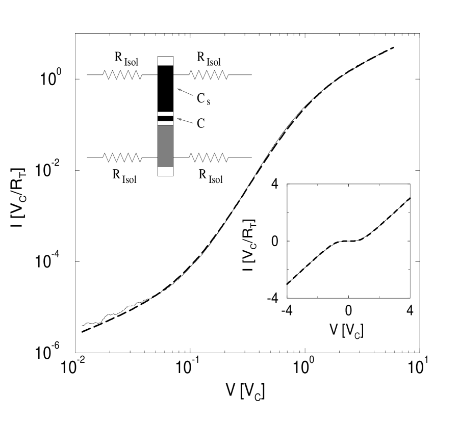
The sample (see upper inset of Fig. 1) is fabricated with a three-level process. First, the resistor level is patterned and a bilayer film of 3nm Cr and 25nm of Au is sequentially deposited without breaking vacuum. An etch window is then patterned over parts of the leads and Au removed to form the Cr wires, which are approximately 100nm wide and have a resistivity of about 10 km. Finally, the junction-level mask is patterned, and the standard shadow-evaporation technique with a vertical offset is used to form the Al/AlOx/Al tunnel junctions (dark rectangles in upper inset). The specific capacitance of 4.5 fF/m2 gives a nominal capacitance for the small junction of about 230 aF. Adding to this is the parasitic capacitance of the leads between the junction and the resistors, which we estimate to be 35 aF based on calculations of the self capacitance of other structures with similar wires [21]. The spaces between the resistors are 1.5 m horizontally and 1.5 m vertically. Calculations show that the isolating resistors can be treated as ideal lumped resistors for frequencies up to 100 GHz. The resistors have nearly temperature-independent, linear - characteristics to the lowest temperature. Their noise properties, measured down to 1.2 K, are found to be consistent with Johnson noise for the range of bias currents used in the data presented below. Measurements are made with the sample enclosed in a liquid-He-filled copper cell located on the temperature-regulated platform of a dilution refrigerator. All leads entering this cell pass though high-attenuation microwave filters[22], which are thermally anchored to the platform. A magnetic field of 1 T is applied to suppress superconductivity in the sample.
The fabrication process, chosen to minimize , results in a secondary series junction with an area (and capacitance ) about 15 times that of the small junction, making the device into an asymmetric transistor, albeit one whose conductance is almost entirely determined by the small junction. The energy change as an electron tunnels through the small junction is given by , where is the island charge and . For the region of interest, , where the current is determined by the forward tunneling rate through the small junction, the voltage for a fixed bias current is minimized for . In this case, and, within the sequential tunneling model, the asymmetric transistor is predicted to behave essentially as a single junction[20]: It has no blockade for , has a blockade voltage when , and exhibits the power-law behavior of Eqs. 1 and 2 with . Both the smaller “bare” resistance of the secondary junction and the much weaker effect of the high impedance environment () ensure that the first junction is the bottleneck for the electron transfer across the device. If the resistance of the (probably leaky) secondary junction is much less than , , and the correspondence between the transistor with and the single junction is even closer, with simply increasing slightly.
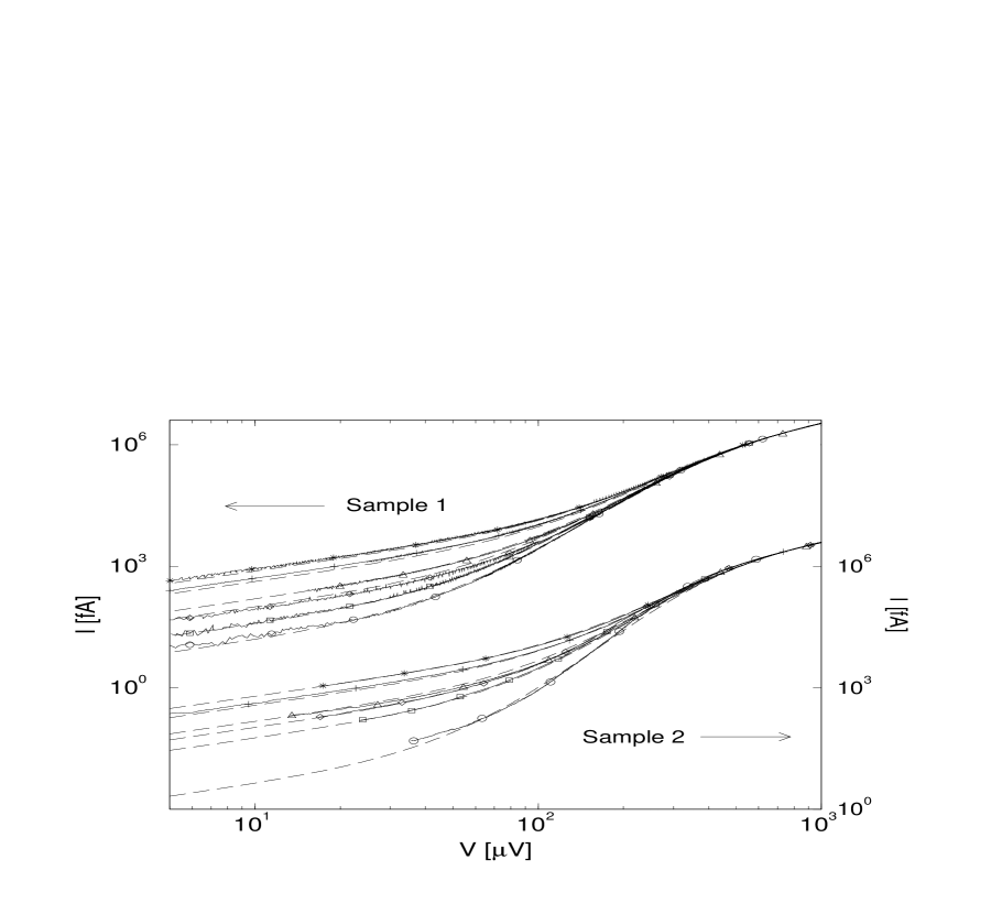
We present data from two samples with nominally identical junctions but with isolating resistors of different length and resistance: 4 m (40 k for sample 1 and 8 m (75 k for sample 2. The parameters for these samples are summarized in Table I. All data are taken with as determined by adjusting the back-plane gate to minimize for . A low-temperature - curve for sample 1 is shown in Fig. 1. The voltage offset, V, due to Coulomb blockade is clearly seen in the linear-scale lower inset. The current variation for is more clearly seen in the main log-log plot, where it is compared with the numerical solution of the theory. The large current suppression () indicates the strong blockade seen in this sample. Figure 2 shows - curves taken at several temperatures for both samples, again compared with the result of numerical solution. One can see that sample 2, which has a larger , has a stronger blockade and a steeper power-law region at the lowest temperature.
The current (dashed lines in Figs. 1 and 2) is calculated using the standard golden-rule approach with the effects of the environment included through the correlation function of phase fluctuations due to the total environmental impedance [17, 18, 19]. We take the real part of this impedance to be: Re where and is the effective junction capacitance corresponding to the experimentally determined value of (see Table I). and are determined from the high-voltage data, where the corrections due to finite temperature and are negligible. The isolating resistance is then used as the only adjustable parameter in fitting the data for , giving an excellent fit over six orders of magnitude in the current. In view of the essentially identical behavior of the transistor with and the single junction, and the impossibility of accurately determining , we treat the sample as a single junction and admit some uncertainty in our comparison of the measured and fitted values of . Table I compares this best-fit value of with the independently measured value. For both samples the best-fit value is approximately 10 k higher than the measured value. This may very well be the resistance of
As noted, the physical basis for the power-law behaviors seen in these samples and in Luttinger liquid is the same. Therefore it is of considerable interest to examine in more detail the region of validity for those behaviors in our devices. While the full theory (Figs. 1 and 2) requires numerical integration, analytical expressions illustrating the power-law behaviors in Eqs. 1 and 2 for the conductance can be derived for the limit and :
| (3) |
where is the zero-bias conductance given by
| (4) |
with () being the cutoff frequency of excitations, and
| (5) |
is the Gamma function. Equation 4 explicitly shows the power-law temperature dependence of () for k. For , the Gamma functions in Eq. 5 can be expanded, yielding the voltage power law .
Equation 3 shows that, at low bias and fixed , the conductance can be scaled to a function of as seen in Fig. 3. The main figure shows this scaled conductance compared to the prediction of Eq. 5 (solid line). The arrows associated with the data sets at different temperatures indicate the points at which , where deviations from the low-voltage approximation begin to appear. For this scaling, has been used as a free parameter at each temperature. The resulting values for for both samples are compared with the numerical results (solid lines) in the inset of Fig. 3 (Note that is scaled to for each sample.). Again, agreement is quite good. Sample 2, which has a larger (see Table I), shows the predicted decrease in and increase in the power-law exponent compared to sample 1. However, the low-temperature approximation (Eq. 4, dashed lines) deviates significantly from the data (and the finite-temperature theory) at . The scaling of voltage with temperature as well as the power-law dependence of on are much more robust, with deviations of less than 15% from Eq. 5 for , independent of temperature and . This fit, along with the strong temperature dependence of , indicates that the heating in is not significant, at least for . For mK, the data become nearly independent of T. We cannot presently rule out experimental artifacts as the explanation for this effect, which requires further study.
In summary, we have measured the -characteristics of resistively isolated tunnel junctions with . We find strong Coulomb blockade with an increase of up to 104 in the zero-bias resistance compared to the high-bias tunnel resistance of the junctions. For temperatures above 60 mK, the results agree well with the theory based on an “environmental” description of the resistor as a collection of oscillators with a linear spectrum. In particular we clearly observe the predicted power-law dependences of and with the power-law exponents dependent on in a manner consistent with the theory.
We thank K.K. Likharev and A. Rylyakov for useful and stimulating discussions. This work was supported in part by AFOSR.
REFERENCES
- [1] Present address: Dept. of Physics and Astronomy, Univ. of Kansas, Lawrence, KS 66045.
- [2] D.V. Averin and K.K. Likharev in Mesoscopic Phenomena in Solids, ed. by B.L. Altshuler, P.A. Lee, and R.A. Webb (Elsevier, Amsterdam, 1991).
- [3] Single Charge Tunneling, ed. by H. Grabert and M.H. Devoret (Plenum, New York and London, 1993);
- [4] L.J. Geerligs, V.F. Anderegg, P.A.M. Holweg, J.E. Mooij, H. Pothier, D. Esteve, C. Urbina, and M.H. Devoret, Phys. Rev. Lett. 64, 2691 (1990).
- [5] P. Delsing, K.K. Likharev, L.S. Kuzmin, and T. Claeson, Phys. Rev. Lett. 63, 1180 (1989).
- [6] A.N. Cleland, J.M. Schmidt, and J. Clarke, Phys. Rev. Lett. 64, 1565 (1990).
- [7] L.S. Kuzmin and Yu. A. Pashkin, Physica B 194-196, 1713 (1994).
- [8] T. Holst, D. Esteve, C. Urbina, and M.H. Devoret, Phys. Rev. Lett. 77, 3889 (1996).
- [9] J.P. Kauppinen and J.P. Pekola, Phys. Rev. Lett. 77, 3889, (1996).
- [10] D. Popovic, C. J. B. Ford, J. M. Hong and A. B. Fowler, Phys. Rev. B, 48, 12349 (1993).
- [11] Since the submission of this manuscript, related work on resistively isloated junctions in the strong tunneling regime has appeared: P. Joyez, D. Esteve, and M.H. Devoret, Phys. Rev. Lett. 80, 1956 (1998).
- [12] C.L. Kane, and M.P.A. Fisher, Phys. Rev. Lett. 68, 1220 (1992).
- [13] F.P. Milliken, C.P. Umbach, and R.A. Webb, Solid State Comm. 97, 309 (1996).
- [14] A.M. Chang, L.N. Pfeiffer, and K.W. West, Phys. Rev. Lett. 77, 2538 (1996).
- [15] M. Grayson, D.C. Tsui, L.N. Pfeiffer, K.W. West and A.M. Chang, Phys. Rev. Lett. 80, 1062 (1998).
- [16] A.O. Caldeira and A.J. Leggett, Ann. Phys. (N.Y.) 149, 374 (1983).
- [17] Yu.V. Nazarov, Pis’ma Zh. Eksp. Teor. Fiz. 49, 105 (1989) [JETP Lett. 49, 126 (1989)].
- [18] M.H. Devoret, D. Esteve, H. Grabert, G.-L. Ingold, H. Pothier, and C. Urbina, Phys. Rev. Lett. 64, 1824 (1990).
- [19] S.M. Girvin, L.I. Glazman, M. Jonson, D.R. Penn, and M.D. Stiles, Phys. Rev. Lett. 64, 3183 (1990).
- [20] G.-L. Ingold and Yu.V. Nazarov, chapter 2 in [3].
- [21] K.A. Matsuoka, K.K. Likharev, P. Dresselhaus, L. Ji, S. Han. and J. Lukens, J. Appl. Phys. 81, 2269 (1997).
- [22] D.J. Flees and J.E. Lukens, Meeting Abstracts, 96-2, 553 (1996) (The Electrochemical society, Pennington, NJ).

| Sample No. | 1 | 2 | |
|---|---|---|---|
| 170 | 152 | ||
| 5.28 | 4.89 | ||
| 455 | 422 | ||
| 71 | 41 | ||
| 0.84 | 0.48 | ||
| 40 | 75 | ||
| 52 | 84 |