Shot Noise Enhancement in Resonant Tunneling Structures in a Magnetic Field
Abstract
We have observed that the shot noise of tunnel current, , in GaSb-AlSb-InAs-AlSb-GaSb double-barrier structure under a magnetic field can exceed . The measurements were done at T=4K in fields up to 5T parallel to the current. The noise enhancement occurred at each of the several negative-differential conductance regions induced by the tunneling of holes through Landau levels in the InAs quantum well. The amount of the enhancement increased with the strength of the negative conductance and reached values up to . These results are explained qualitatively by fluctuations of the density of states in the well, but point out the need for a detailed theory of shot noise enhancement in resonant tunneling devices.
pacs:
PACS Numbers: 73.40.Gk, 73.50.Td, 73.50.Jt, 73.20.DxSince shot noise is sensitive to correlation effects that result from Pauli exclusion principle and the Coulomb interaction between charged particles, noise measurements can give information about the kinetic of electrons in a conductor. The realization of this fact has spurred recent interest in shot noise in a variety of systems [1], including the double-barrier resonant-tunneling diode (RTD).
The current-voltage characteristic (I-V) of an RTD usually has a quasi-triangular shape, with an initial region of positive differential conductance (PDC) before the current peak, followed by a sharp region of negative differential conductance (NDC) just after the peak. So far, most studies of shot-noise have focused on the PDC region, probably because experimentally the NDC region is often masked by an external instability that depends on the circuit to which the diode is connected. Measurements in GaAlAs-GaAs-GaAlAs RTDs have shown a significant noise suppression relative to the ”full” shot noise ( is the electron charge and I the tunneling current), which has been explained by correlation between tunneling electrons [2].
The deviation of the actual shot noise from is quantified by a Fano factor, defined as the ratio of the noise spectral density, , to the full shot noise. Using either a quantum-transport [3] or a semiclassical theory [4] it has been shown that the Fano factor can be expressed in terms of the tunneling probabilities and , through the two potential barriers:
| (1) |
The value for ranges from , for very asymmetric barriers, to , when . For completely incoherent transport we can view the two barriers as two resistances in series and if each resistance generates full shot noise then tunneling probabilities in (1) are replaced by differential resistances of the barriers [5]. As Landauer [6] has pointed out, the maximum noise suppression is readily obtained then for two identical diodes in series.
The few results available in the NDC region exhibit a behavior very different from the suppression found in the PDC region. Li et al.[2] showed enhancement of noise in the NDC region, although, their focus being on noise suppression in the PDC region, they did not discuss that result in detail. Brown [7] has reported an enhancement of the current noise for a single voltage in the NDC region, confirmed by Iannaccone et al. [8] in measurements for voltages throughout the entire NDC region. They have explained their observation in terms of correlation produced by shifts in the density of states for tunneling, and have accounted for the noise enhancement with a calculation that extends a formalism originally developed for noise suppression in the PDC region [9].Theoretically, Pytte and Thomas studied long ago the fluctuations in Gunn diodes, whose I-V characteristics are similar to those of resonant-tunneling structures, but they did not consider in detail the NDC region [10].
In this paper we report the observation of multiple peaks in the noise characteristics of a RTD when a magnetic field is applied parallel to the tunnel current. Similarly to previous works, we find that whenever there is an NDC region in the I-V characteristics of the diode the noise is enhanced over its background and shows a peak. But the fact that in our experiments the number of NDC regions and their strengths depend on the intensity of the magnetic field has allowed us to correlate directly the enhancement of shot noise with the corresponding NDC values, which should be valuable to theories aiming at explaining in detail the enhancement of shot noise.
The experiments have been done in a type II GaSb-AlSb-InAs-AlSb-GaSb double-barrier structure. The top of the valence band of GaSb (electrode) lies above the bottom of the conduction band of InAs (quantum well). As a consequence, there is a charge transfer between the two materials, with two-dimensional (2D) electrons accumulating in the InAs well and comparable number of 2D holes accumulating on the GaSb side of the GaSb-AlSb interfaces. AlSb barriers provide charge confinement and separation. When a voltage is applied between the GaSb electrodes, holes tunnel from the emitter to the collector via a quantum state in the conduction band of InAs [11] (See upper inset of Fig. 1). With increasing voltage more states are available for tunneling and the current increases, until misalignment between states prevents further tunneling and the current abruptly goes to zero [12]. Our structure is different from the conventional GaAs/AlGaAs heterostructure in that at large bias the quasi-Fermi level in the well is always above the valence band of the emitter. Thus, it is possible for holes tunneling into the well to be scattered inelastically above the emitter valence band, in which case Pauli exclusion principle has no effect and correlation is only due to Coulomb repulsion.
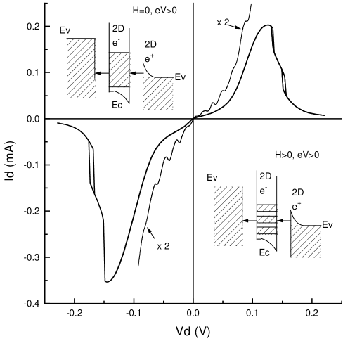
Figure 1 shows the experimental I-V characteristics, at T = 4.2K, for a 20m diode that consists of the following regions: 3,000Å p+ GaSb (Na=2x1018 cm-3); 500Å p GaSb (1x1017 cm-3); 50Å undoped GaSb; 50Å undoped AlSb; 150Å undoped InAs; 50Å undoped AlSb; 50Å undoped GaSb; 500Å p GaSb (1x1017 cm-3), (2x1018 cm-3) p+ GaSb substrate. The small current asymmetry between both voltage polarities in Fig.1 is possibly due to an effective asymmetry between the two AlSb barriers. The hysteresis regions are from instabilities in the circuit external to the diode and will not be discussed here.
Also shown in Fig.1 is the I-V characteristic when the diode is subject to a magnetic field parallel to the tunnel current. At the Landau-level energies the field creates sharp maxima in the density of states of the well and deep minima (or gaps) in between (See lower inset of Fig. 1). As a result, the I-V characteristic exhibits distinct features associated with tunneling via individual Landau levels. These features become more pronounced with increasing field and eventually show NDC, as illustrated in Fig. 1 for H = 3T. Moreover, for a fixed field, especially if it is weak or moderate, the strength of those features varies. This variation (whose origin is not clear), combined with that offered by the change in field, allows for a wide range of stable NDC regions.
The shot noise of the diode was measured at T = 4K, with the device grounded at one end and in series with a load resistor R0 close to it. (The value of R0 was 420 up to a field of 3T, and 77 for 4T and 5T.) The sample was connected with low-impedance coaxial cables to a room-temperature circuit which included a R1 = 110 k resistor through which an AC signal was applied to the sample and measured simultaneously with the noise spectrum. The voltage noise across the device in parallel with the load resistor was measured by a low voltage noise preamplifier (voltage noise of 1.4nV/Hz1/2 and noise resistance of about 1k) followed by a spectrum analyzer with a 100kHz frequency band.
The procedure for calculating the current noise of the device was as follows. First the voltage noise of the preamplifier and the leads (measured separately) was subtracted from the output noise, and then the result was divided by the normalized AC signal, which is the product of the differential resistance and coefficient of amplification. Finally, the small background current noise of the preamplifier was subtracted. The spectrum of the noise was ”white” up to 100kHz. When repeated for both directions of the voltage sweep (each took several hours), the experimental curves were reproducible, which indicates stability of both the sample and the electronics.
At zero magnetic field and small tunnel currents, the measured shot noise for the PDC region follows the value for uncorrelated electrons (), as shown in Fig. 2. For larger currents the noise is significantly suppressed, but eventually increases, crosses the classical value and then is enhanced over the value. For positive bias the suppression is about one-half of the full shot noise, as expected for a symmetric double barrier structure [13], but for negative bias the suppression is larger. Although we do not know the origin of this large suppression, we have no reason to believe that is related to the materials configuration of our heterostructure. To our knowledge, such a large suppression has been reported only once [7] and, with the exception of a numerical calculation [14], existing theories do not predict noise reduction larger than one-half [9, 15].
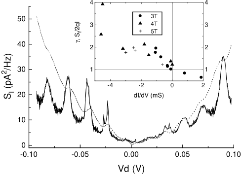
In the presence of a small field the noise in the diode is modified in two ways, as seen in Fig.2 for H = 3T. There is a deviation of the 3T background from H=0 curve, especially at low currents, where the field suppresses shot noise beyond . The most visible change is the appearance of sharp peaks superimposed on a noise background. Some of the noise peaks are as large as to even exceed the full shot noise value. The pronounced loop of the peak at -0.05mA indicates that the current itself peaks at this value in the I-V characteristic, as is better seen on Fig. 3, where the measured noise is plotted as a function of bias along with the quantity .
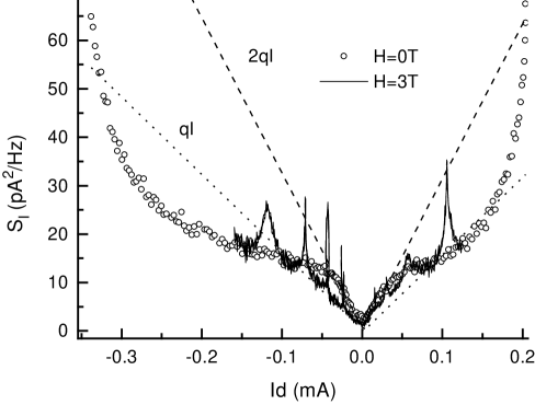
The correlation between peaks in the noise and the features in the I-V characteristic is apparent in Fig. 3: the voltages at which the noise peaks occur correspond to those of negative (or close to negative) differential conductance in the current. Moreover, the values of the peak maxima in the noise spectrum are correlated with the values of concomitant differential conductance features: the smaller the conductance, the larger the noise peak. Thus, when the conductance is small but still positive, the noise peak is above the suppressed noise value but below . (See, for instance, the peak at about -0.08V.) When the conductance is around zero full shot noise is approximately recovered. (See the peak at 0.08V). And when the conductance becomes negative (for example, at -0.04V and -0.06V) the noise is enhanced well beyond . It should also be noted that the peaks that show this enhancement pass the value at voltages at which the conductance is approximately zero.
This behavior can be explained by realizing that noise is sensitive to the variation of the density of states with a change of the number of electrons in the well [8]. Let us consider first the case of zero magnetic field, in which the density of states is constant above the edge provided by the quantum-state energy. The tunnel current increases as long as the voltage is such that the quantum-state energy is below the effective edge of the valence band of the emitter electrode (Upper inset of Fig. 1). When a hole from the GaSb emitter tunnels into the InAs well, the density of states in the well goes down and the number of states available for subsequent tunneling holes is smaller. In this case, there is a correlation between tunneling holes (in other words, there is a negative feedback between tunneling holes) and noise is suppressed. But when the voltage is such that the quantum-state energy is just below the emitter valence-band edge, the feedback is positive: by going down in energy when a hole tunnels, the density of states is now increased and additional holes can tunnel. This opposite correlation between holes enhances shot noise, and the rapid increase of noise in Fig. 2 beyond 0.16 mA (for positive current) and -0.25 mA (for negative current) reflects such an enhancement.
An external magnetic field modifies drastically the density of states in the well from a step function to a series of quasi-delta functions (Landau levels). Although for the moderate fields considered here it may be more appropriate to speak of a step function modulated by an oscillatory component, for simplicity in this discussion we assume a density of states that consists of Gaussian distributions centered at the Landau-level energies, the widths of which are a measure of the energy broadening of the states. With increasing voltage, the successive alignment of the emitter edge with the centers of those Gaussians gives rise to peaks in the tunnel current, followed by regions of negative differential conductance. Each of these regions, then, results from an alignment of the emitter with a decreasing density of states. If a hole tunnels now into the well, the density of state goes down and the emitter becomes aligned with a portion of the distribution that can accommodate more states, thus favoring the tunneling of a second hole and therefore enhancing shot noise. The sharper the density-of-states distribution (because of higher field or reduced broadening), the more pronounced is the NDC and the stronger is the enhancement of noise.
The direct connection between shot noise and negative differential conductance is seen in the insert of Fig. 3, where we have plotted the Fano factor for the maxima of the noise peaks versus , for three values of the magnetic field. The graph shows a monotonic increase of noise above () with increasingly negative conductance, from when the conductance is zero. Although the value of seems to level off at around 2 before resuming its increase up to a maximum value of 4, more experiments are needed before the details of such a behavior are confirmed. Previous experiments at zero field have yielded for values between 2 and 9 (Refs. 2, 7, 8).
Iannacone et al. [8] have expressed the Fano factor in terms of the characteristic times , for the processes of generation and recombination of electrons in the well:
| (2) |
and used this expression to explain noise enhancement. When is zero full shot noise is recovered, and as it becomes negative in the NDC region (while remains positive) shot noise is enhanced. This expression can be understood in simple terms with the two-resistance analogy mentioned above, by which the characteristic times of Eq. (2) are replaced by the differential resistances of the two barriers. Then, the resistance of the emitter barrier is infinite at the resonance and negative in the NDC region, and becomes one and larger than one, respectively.
In conclusion, we have shown that by changing the shape of the density of states in the quantum well with a magnetic field the value of the shot noise relative to the classical value can change from suppression to enhancement. A quantitative comparison between the prediction of Eq. (2) and the experimental results of Fig. 3 is not possible without knowing the transition rates as a function of the number of holes in the well. A calculation of these rates along the lines of Ref. 8 is not trivial, especially in the presence of a magnetic field. In any case, the validity of Eq. (2) is somewhat surprising since it follows from a linearization of the transition rates in the NDC region, in which large charge fluctuations are expected [16]. A microscopic theory that includes these non-linear effects seems therefore needed.
The authors have benefited from discussions with R. Landauer. This work has been sponsored by the Department of Energy (DOE’s Grant No. DE-FG02-95ER14575).
REFERENCES
- [1] For a recent review, see M. J. M. de Jong and C. W. J. Beenakker, cond-mat/9611140 (1996).
- [2] Y. P. Li, A. Zaslavsky, D. C. Tsui, M. Santos, and M. Shayegan, Phys. Rev. B 41, 8388 (1990).
- [3] L. Y. Chen and C. S. Ting, Phys. Rev. B 43, 4534 (1991); M. Buttiker, Physica B 175, 199 (1991).
- [4] J. H. Davies, P. Hyldgaard, S. Hershfield, and J. W. Wilkins, Phys. Rev. B 46, 9620 (1992); L. Y. Chen and C. S. Ting, Phys. Rev. B 46, 4714 (1992).
- [5] C. W. J. Beenakker and M. Buttiker, Phys. Rev. B 46, 1889 (1992).
- [6] R. Landauer, Physica B 227, 156 (1996).
- [7] E. R. Brown, IEEE Trans. Electron Devices 39, 2686 (1992).
- [8] G. Iannaccone, G. Lombardi, M. Macucci, and B. Pellegrini, Phys. Rev. Lett. 80, 1054 (1998).
- [9] G. Iannaccone, M. Macucci, and B. Pellegrini, Phys. Rev. B 55, 4539 (1997).
- [10] E. Pytte and H. Thomas, Phys. Rev. 179, 431 (1968).
- [11] Equivalently, the process can be seen as electrons tunneling out of the InAs well to the valence band of GaSb, followed by electrons from the other GaSb electrode tunneling into the InAs well. See, for example, Ref. 12.
- [12] E. E. Mendez, H. Ohno, and L. Esaki, Phys. Rev. B 43, 5196 (1990); E. E. Mendez, J. Nocera, and W. I. Wang, Phys. Rev. B 45, 3910 (1992).
- [13] H. C. Liu, J. Li, G. C. Aers, C. R. Leavens, M. Buchanan, and Z. R. Wasilewski, Phys. Rev. B 51, 5116 (1995); H. Birk, M. J. M. de Jong, and C. Schonenberger, Phys. Rev. Lett. 75, 1610 (1995).
- [14] M. M. Jahan and A. F. Anwar, Solid State Electronics 38, 429 (1995).
- [15] L.Y.Chen, Phys. Rev. B 48, 4914 (1993); J. H. Davies, J. C. Egues, and J. W. Wilkins, Phys. Rev. B 52, 11259 (1995).
- [16] R. Landauer, private communication.