Two-dimensional arrays of low capacitance tunnel junctions:
general properties, phase transitions and Hall effect
Abstract
We describe transport properties of two-dimensional arrays of low capacitance tunnel junctions, such as the current voltage characteristic and its dependence on external magnetic field and temperature. We discuss several experiments in which the small capacitance of the junctions plays an important role, and we also describe the methods for fabrication and measurements.
In arrays where the junctions have a relatively large charging energy, ( when they have a low capacitance) and a high normal state resistance, the low bias resistance increases with decreasing temperature and eventually at very low temperature the whole array may become insulating even though the electrodes in the array are superconducting. This transition to the insulating state can be described by thermal activation, characterized by an activation energy. We find that for certain junction parameters the activation energy oscillates with magnetic field with a period corresponding to one flux quantum per unit cell.
In an intermediate region where the junction resistance is of the order of the quantum resistance and the charging energy is of the order of the Josephson coupling energy, the arrays can be tuned between a superconducting and an insulating state with a magnetic field. We describe measurements of this magnetic-field-tuned superconductor insulator transition, and we show that the resistance data can be scaled over several orders of magnitude. Four arrays follow the same universal functin provided we use a modified scaling parameter. We find a critical exponent close to unity, in good agreement with the theory.
At the transition the transverse (Hall) resistance is found to be very small in comparison with the longitudinal resistance. However, for magnetic field values larger than the critical value. we observe a substantial Hall resistance. The Hall resistance of these arrays oscillates with the applied magnetic field. Features in the magnetic field dependence of the Hall resistance can qualitatively be correlated to features in the derivative of the longitudinal resistance, similar to what is found in the quantum Hall effect.
I Introduction
The electrical transport in two-dimensional (2D) arrays of small Josephson tunnel junctions can be described either in terms of charges or in terms of vortices Mooij/Schon-LH ; Fazio/Schon . Transport of charge generates a current which acts as a driving force for the vortices. The charge transport may be obstructed by a large charging energy, , being the capacitance of the individual junction. On the other hand, transport of vortices generates a voltage which acts as a driving force for the charges. The vortex transport may be hindered if the Josephson coupling energy is large. At low temperature the Josephson coupling energy is given by , where is the normal state resistance of the individual junctions, k is the quantum resistance , and is the superconducting energy gap of the electrodes.
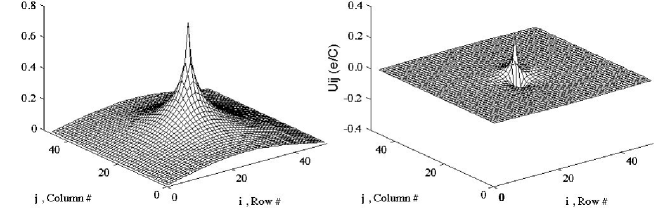
Adding a single charge to an electrode in the array gives rise to an electrostatic potential distribution which is sometimes referred to as a charge solitonBakhvalov-2D . A missing charge gives rise to the counterpart, an anti-soliton. The charge solitons can move in the array by single-charge tunnel events. When the electrodes are superconducting, both Single Electron Solitons (SES) and Cooper Pair Solitons (CPS) can exist. An exact calculation of the potential distribution in a junction array assuming only nearest neighbor coupling, is shown in Fig. 1, for two different cases: A single electron in the center of the array, giving rise to a SES, and the fundamental excitation, a soliton/anti-soliton pair at adjacent electrodes. The size of the soliton is given by as long as . is the capacitance between an electrode in the array and infinity. However if is of the order of the nearest neighbor approach is not a good approximation Orlando-APL96 .
On the other hand, due to the existence of a macroscopic phase of the superconductor, a vortex, i.e. a phase winding of 2, with an associated magnetic flux quantum , can exist in a loop of the array. In a two-dimensional (2D) array of small Josephson tunnel junctions the duality between charges and vortices is especially pronounced. Therefore it is a very suitable object to study the dynamics of both charges and vortices.
The arrays which have high junction resistance, and large charging energy, , become insulating at low temperature due to the Coulomb blockadeAverin/Likharev ; LesHouches , regardless of whether the electrodes are superconducting or normal.
In the opposite limit, and , superconductivity prevails and the resistance goes to zero at low temperature. In this limit where the Josephson energy dominates, vortices act as classical or quasi-classical particles and there is a large number of papers describing such systems theoretically Mooij-NATO86 ; Mooij/Schon ; Frascati-95 ; Minnhagen-RMP as well as experimentally Voss/Webb ; LAT ; Wees-PRB87 ; Tighe-PRB91 ; vdZant-PRB93 ; Rzchowski-PRB94 ; CCD-PRB96 With normal electrodes and the array goes insulating at low temperature while in the opposite limit , the array stays resistive even down to very low temperature.
In this paper we will concentrate on the arrays where the charging energy is comparable to or larger than the Josephson coupling energy, and where the junction resistance is of the order of or larger than . Throughout this paper, we will refer to an array with normal electrodes as being in the N-state, and to an array with superconducting electrodes as being in the S-state.
If the interaction between the charges (or vortices) is logarithmic, the transition to the insulating (superconducting) state would be of the Kosterlitz-Thouless-Berezinskii (KTB) typeKT(B) ; (KT)B . As the temperature is increased, an insulating 2D array can undergo a charge unbinding transitionMooij-PRL90 at some transition temperature, which results in a conductive state. Likewise, a superconducting array can undergo a vortex unbinding transition to a resistive state. It has been shown that the superconducting transition can be described as a vortex unbinding, KTB transitionVoss/Webb . In more recent years there has also been a lot of interest in arrays where the dynamics is best described in terms of charges Mooij-PRL90 ; GeerligsPhysicaB ; Geerligs-PRL89 ; CCD-PhysicaScripta ; Delsing-SQUID91 ; Tighe-PRB93 ; Delsing-PRB94 ; Kanda/Kobayashi . In several papers there has been a discussion whether the observed transition to the insulating state can be described as a KTB transition as wellMooij-PRL90 ; Delsing-SQUID91 ; Tighe-PRB93 . In a paper by Tighe et al.Tighe-PRB93 it was pointed out that the transition could be well described by thermal activation of charge solitons. Comparing results of three different groupsMooij-PRL90 ; Delsing-SQUID91 ; Tighe-PRB93 , they found an activation energy in the N-state, a value which can be theoretically justified. They also suggested that in the S-state at , should be , where is the superconducting energy gap at and . An interesting new result is that of Kanda and Kobayashi Kanda/Kobayashi where they find a thermal activation behavior at higher temperatures but a stronger dependence at lower temperature in the N-state. An interesting theoretical development in this field is a recent paper by Feigelman et al.Feigelman , where they treat the posibility of parity effects 2D arrays. In section IV we will describe measurements where we have investigated the transition to the insulating state extensively.
For arrays in the intermediate regime ( and ) which just barely go superconducting, a small magnetic field can drastically change the low bias resistance and in fact drive the array into the insulating state vdZant-PRL92 . In a theoretical description of this effect Fischer-PRL90 , the field induced excess vortices drive the system from a vortex glass superconducting phase into a Bose-condensed insulating phase. The zero-magnetic-field KTB vortex-unbinding transition is replaced by a field-tuned vortex-delocalization transition. A superconductor-insulator(SI) transition can also be driven by other external variables such as electric field Bruder ; Lafarge-95 or dissipation Rimberg-PRL97 . In Section V we show experiments on the magnetic-field-tuned superconductor-insulator transition. The zero bias resistance, was measured as a function of temperature and frustration. The frustration, is defined as the magnetic field normalized to , where is the field corresponding to one flux quantum per unit cell in the array. The scaling curves demonstrate how , plotted as a particular function of and , display a transition from insulator to superconductor. According to theory the resistance at the critical frustration should be universal and equal to . From the data of four different arrays we find a value which is of the order of but sample dependent. We can also deduce a dynamic exponent close to unity, which is in agreement with the theory Fischer-PRL90 .
Right at the critical frustration, the Hall resistance is very small compared with the longitudinal resistance, indicating a small Hall effect at the SI transition. However for frustration values larger than the critical frustration the Hall resistance can be relatively large. Hall measurements in both conventional superconductors Graybeal-PRB94 ; Smith-PRB94 and high- superconductors Samoilov-PRB94 ; Harris-PRB94 have shown a sign reversal of the Hall resistivity in the vicinity of the superconducting transition temperature , where the samples are in a mixed state. Hall measurements have also been performed on disordered superconductors near the superconductor-to-insulator transition Paalanen-PRL92 . In Section VI we present the frustration dependence of the longitudinal resistance and the Hall resistance . Both the longitudinal and Hall resistance are periodic functions of the magnetic filed, and the Hall resistance changes sign at several magnetic fields within one period. We also describe the dc measurements of longitudinal voltage and the Hall voltage as a function of bias current .
II Sample Fabrication and Measurements
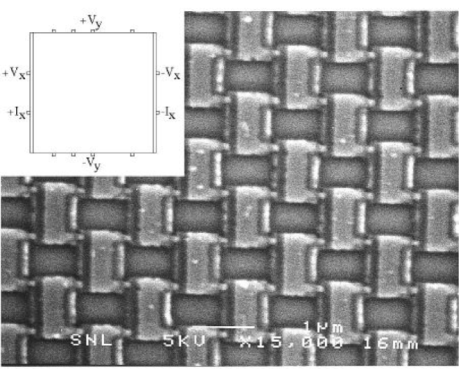
The arrays are fabricated on unoxidized silicon substrates, using a combination of photo- and electron-beam-lithography and an angle evaporation technique. Aluminum is used for both top and bottom electrodes. The number of junctions in each row, N, is the same as the number of junctions in each column, with N ranging between 10 and 168. Therefore, the array resistance equals the individual junction resistance, assuming a homogeneous array.
The samples are made in two steps. First a gold contact pattern is made with conventional photo lithography, and then the actual array is made with electron-beam lithography The contact pattern contains a large number of 7x7 mm2 chips distributed over a 2 inch wafer area, each with 16 contact pads leading to a central area of 160x160 m2. A double metal layer of 20 nm chromium-nickel and 80 nm gold is evaporated and the redundant metal is lifted off in acetone. The chromium-nickel film makes the gold stick better to the surface.
A double layer e-beam resist consisting of a 210 nm thick bottom layer of P(MMA/MAA) copolymer is spun onto the wafer and a 60 nm thick top layer of PMMA(950k) is used. The chip is mounted in an e-beam lithography instrument and the central area of each chip is exposed using the array pattern. A current of 20-30 pA corresponding to a beam size of about 10 nm is used. The beam voltage is 50 kV and the area dose is 160-200 C/cm2.
Each chip is then developed in two different developers: first for 10-20 s in the PMMA developer which consists of a 1:3 mixture of toluene and isopropanol, then for 20-40 s in the copolymer developer which consists of a 1:5 mixture of ethyl-cellosolve-acetate (ECA) and ethanol. As an alternative the nontoxic mixture of 5-10 % water in isopropanol can be used to develop both layers in one step, with a development time of 1-2 minutes.
After development, the resist mask contains an undercut pattern with suspended bridgesNiemeyer ; Dolan which will be used to form the junctions. By depositing bottom and top electrodes from different angles the overlap can be controlled. The base and top electrodes are evaporated from tungsten boats, while the substrate holder is tilted at two different angles () to give the desired overlap. Before the top electrode is deposited, a tunnel barrier is formed by introducing 0.01-0.1 mbar of oxygen to the chamber for 3-10 minutes, by adjusting the oxidation parameters we get the desired junction resistance.
A drawback with the angle evaporation technique is that a relatively large junction is formed in series with the small tunnel junction, see Fig. 3. The effect of this larger junction can in most cases be neglected, if its area is much larger than the area of the smaller junction. This is easy to make, but this requirement limits the minimum unit cell size of the array, which in turn decreases the soliton size.
The fabrication procedure results in junctions with normal state resistances in the range 4 to 150 k, capacitances of the order of 1 fF, and V per junction. The typical unit cell size is of the order of m2 These values are deduced from the -characteristics, assuming an offset voltage of (for a discussion of the offset value see Ref.Tighe-PRB93 ). The Josephson coupling energies of the individual junctions are determinedAmbegaokar/Baratoff from and . The superconducting transition temperature for the aluminum is in the range of 1.35 to 1.60 K.
The self capacitance of each electrode depends on the size of the electrode and the size of the array, and can be estimated to be of the order 10-20 aF for the smaller arrays (#2 and #3) and about 2 aF for the other arrays. This results in a soliton size in the range of 11 to 35, measured in units of the lattice spacing.
The most important parameters of the 2D arrays described in this paper are listed in Table 1. The arrays are divided into 3 groups. Arrays #1-3 show a decreasing resistance for decreasing temperature, and are referred to as the ”superconducting” arrays. They have a low resistance, and a relatively large Josephson coupling energy, .
Arrays #4-8 show also go superconducting at low temperature, but they display the magnetic field tuned SI transition, and are referred to as the ”intermediate” arrays. They have and .
Arrays #9-15 show an increasing resistance for decreasing temperature, and are referred to as the ”insulating” arrays. They have a high resistance, k and a relatively small Josephson coupling energy, .
| # | |||||||||
|---|---|---|---|---|---|---|---|---|---|
| 1 | 112 | ||||||||
| 2 | 20 | ||||||||
| 3 | 10 | ||||||||
| 4 | 146 | ||||||||
| 5 | 168 | ||||||||
| 6 | 146 | ||||||||
| 7 | 168 | ||||||||
| 8 | 146 | ||||||||
| 9 | 146 | ||||||||
| 10 | 80 | ||||||||
| 11 | 80 | ||||||||
| 12 | 100 | ||||||||
| 13 | 100 | ||||||||
| 14 | 80 | ||||||||
| 15 | 100 |
The arrays are mapped onto a so called quasi-Schmid diagramSchmid ; quasiSchmid in Fig. 2, showing the and the parameters of each array. The and values in the range 0 to are scaled onto the horizontal and vertical axes in the range 0 to 2, using the function f(z)=2z/(1+z). The diagonal line represents , i.e. where the charging energy for a Cooper-pair is equal to 2. The dotted line represents the border to the insulating region predicted by Fazio and Schön Fazio/Schon . The dashed line corresponds to a Stewart MacCumber parameter of . Above this line a classical Josephson junction (in the upper right part of the diagram) shows hysteresis Stewart ; MacCumber .
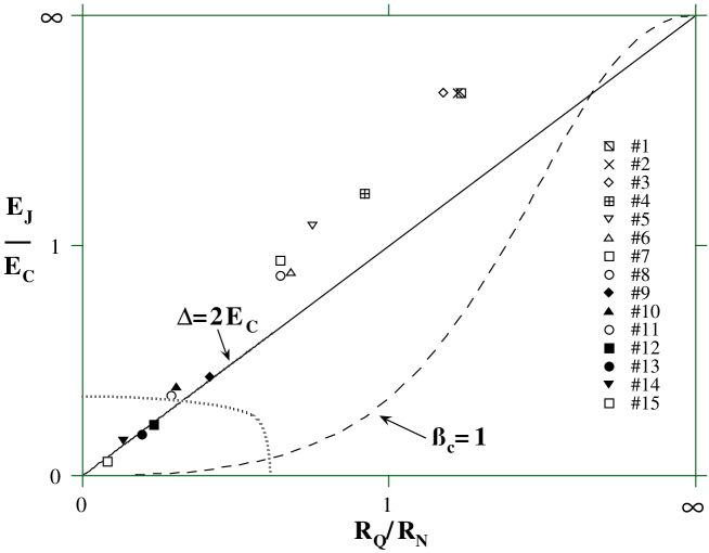
Our classification of the “insulating” arrays roughly agrees with the classification suggested by Fazio and SchönFazio/Schon shown as a dashed line in Fig. 2. However, a few of the arrays (#9-11) which show ”insulating” behavior fall slightly outside the insulating area predicted by Fazio and Schön.
In Section IV, we will concentrate on the ”insulating” arrays, but we will also present the N-state properties of the ”superconducting” arrays. The N-state may be thought of as lying on the x-axis of the diagram in Fig. 2. Sections V and VI will discuss the “intermediate” arrays.
Fig. 3 shows a typical sample, and the inset shows the probe layout for the Hall measurements. There are four Hall probe pairs situated at 1/6, 1/3, 1/2 and 5/6 the distance between the ends of the array. Each Hall probe is actually an array of junctions, with the outer side shorted by a strip from which the Hall voltage is taken. In this way we can reduce the influence on the sample behavior arising from the presence of the voltage probes, and we are less sensitive to local defects possibly occurring in the probe. The resistance of the probe arrays is presumably similar to that of the array itself. This resistance is much smaller than the input impedance of our voltage amplifiers.
The measurements are performed in a dilution refrigerator which is situated in an electrically shielded room. A magnetic field up to about 1400 G is applied perpendicular to the substrate. The magnetic field needed to produce one magnetic flux quantum per unit cell, , varied between 10.4 G and 43.1 G for the different arrays. This is much less than the critical magnetic field, ( G), which was needed to bring the aluminum electrodes into the N-state.
All measurements are made with the biasing and the measurement circuitry symmetric with respect to ground. The current-voltage()-characteristics of the arrays are recorded at temperatures down to about 25 mK. The threshold voltages are deduced from the IVC measured as the voltage at which the current has dropped to two times the noise level (going from large bias). The rms current-noise determined at low voltage is typically of the order of 0.1 pA or less.
For the insulating arrays we deduce the zero bias resistance from the -characteristics. For the “superconducting” and “intermediate arrays”, can also be measured with an ac-technique using lock-in amplifiers, with excitation currents in the range 0.01-3 nA, and frequencies of the order of 10 Hz.
The longitudinal voltage is measured at the superconducting strips at the ends of the array, and the Hall voltage is measured on the probes located on opposite sites of the array. The Hall data presented here were measured from the probes located in the center of the array, see the inset of Fig. 3
III Current voltage characteristics
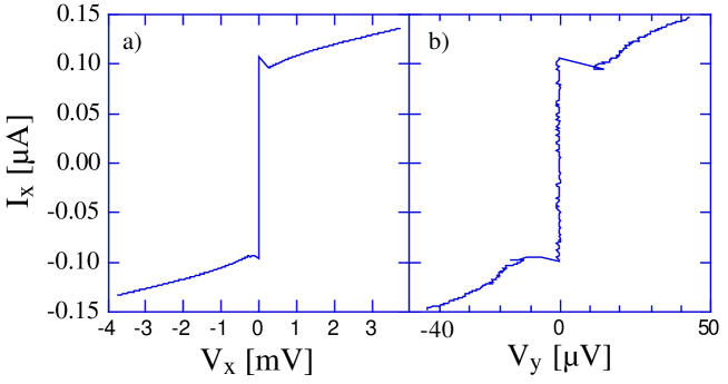
The large scale -characteristics of the arrays are very similar for the 11 arrays and they resemble the -characteristics of a single high resistance Josephson junction. In the S-state there is a sharp rise in the conductance at a voltage . At high voltages the -characteristics are linear and there is the usual offset voltage which is due to the Coulomb blockade Averin/Likharev ; LesHouches . In the N-state the gap feature disappears but the offset voltage remains.
For low bias in the S-state, the -characteristics differ drastically for the different arrays. Qualitative similarities can be found between these -curves and those of single junctions biased through high impedance resistors Haviland-ZPB . Arrays #1-8 show a supercurrent-like feature at low bias, and decreases for decreasing temperature. Arrays #9-15 show a Coulomb blockade feature at low bias, and increases for decreasing temperature.
III.1 The threshold voltage
The threshold voltage is the voltage at which solitons can be injected into the array. According to theory Bakhvalov-2D , the threshold voltage for injection of SESs in the N-state should be
| (1) |
for a symmetrically biased array with . It is important to make the distinction between symmetric and asymmetric (one side grounded) bias of the array, since the latter gives a factor of two lower threshold voltage. However, it has been show by Middelton and Wingreen Middelton/Wingreen that the background charges modifies the picture and that the threshold voltage actually scales with the length of the array if the effect of random background charges is taken into account.
In the N-state, all arrays show Coulomb blockade feature at low temperature and low bias, but the threshold is smeared. However there is no sharp threshold voltage in the N-state for most of the arrays. Only for array #15 , which has the largest , we can deduce a threshold voltage of about 0.25 mV(see Fig. 4). Note that the onset of current occurs at a substantially higher voltage for intermediate magnetic fields. For those fields however the onset was more gradual. A similar behavior was observed in all of the ”insulating” arrays.
All of our arrays were symmetrically biased and for array #15 we get a theoretical value of mV, according to Eq. 1. The fact that the measured value is substantially lower than the theoretically predicted one, is consistent with the picture that quantum fluctuations effectively lower the energy barrier for injection of charge Delsing-PRB94 .
In the S-state there was a sharp threshold for all the ”insulating” arrays, except for arrays #10 and #11. is shown as a function of for four of the arrays in Fig. 5. For several of the arrays oscillates with , demonstrating that Cooper pair solitons are injected at low magnetic fields. The period of oscillation corresponds to one flux quantum per unit cell and agrees well with the values of the different arrays. The oscillations in correspond to the oscillations in activation energy, described in Section IV, and the oscillation peaks in and occur at the same values (compare Figs. 8 and 5). For increasing magnetic field the threshold voltage increases and peaks at a field in the range of 250 to 450 G, which is well below the critical field for the electrodes. then decreases rapidly at larger .
The threshold voltage in the S-state has, to our knowledge, not been described theoretically in the literature. However, following the arguments in Ref.Bakhvalov-2D , and neglecting the Josephson coupling energy, we can estimate for two different situations. For direct injection of Cooper pair solitons, we get a threshold voltage which is two times higher than the value for single electron solitons, . The other possibility is that a Cooper-pair is broken up and then a single electron is injected. Then the threshold would be for the case of symmetric bias. For all our arrays at , and therefore we would expect injection of Cooper pairs to be responsible for the threshold.
This agrees well with our observation of the oscillating at low magnetic field. The increase of with increasing magnetic field can be understood in the following way. Since , and thereby , decreases with increasing magnetic field it becomes harder to inject Cooper-pairs, and therefore increases. At some magnetic field the threshold for single electrons will become equal to that for Cooper-pairs () and we would expect a crossover from Cooper-pair injection to single electron injection. This is observed in all the samples as a peak in at magnetic fields in the range 250 to 450 G. Beyond this crossover decreases as a function of increasing , due to the decreasing .
To get a more quantitative description, other effects depending on the array size and the background charge, as well as co-tunneling and the Josephson coupling, would have to be included. The fact that the observed values at are generally lower than the ”theoretical” value , can possibly be explained if the Josephson coupling energy is taken into account. A step in this direction is a recent paper on 1D-arrays where the threshold dependence on is discussed Haviland/Delsing . The current above the threshold has been analyzed using scaling theory by Rimberg et al. Rimberg-PRL95 .
III.2 Hall voltages
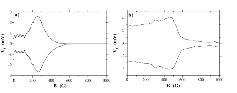
In an array which is strongly superconducting there is no Hall voltage since the Hall probes would be shorted. In an array with a strong Coulomb blockade the whole array is insulating and therefore the Hall probes are effectively disconnected, and no Hall voltage can be measured. Therefore it is not surprising that it is only the “intermediate” arrays which show some Hall voltage. In Fig. 6a we see the characteristics for sample #5 which shows a sharp dip in the current before entering the flux-flow regime, characterized by being proportional to . The curve, shown in Fig. 6b, displays a very similar feature, but the Hall voltage is about two orders of magnitude smaller. As the current is reversed, the Hall voltage changes sign as expected.
In the flux-flow regime, both and increases linearly with applied current until the longitudinal voltage reaches the sum gap voltage of the entire array ( mV). At this point, the Hall voltage reaches a maximum of about 0.2 mV and then starts to fluctuate, gradually decreasing almost to zero. At still higher currents, the Hall voltage displays rich structure, which can also be seen in the derivative of with respect to .
At very high currents, when is on the normal resistance branch of the curve, the Hall voltage also increases linearly with the applied current, with slope . Because this slope is a small fraction of (0.02% for array #5 and 0.1% for array #7) we conclude that small non-uniformities exist in the array. For array #7, the Hall voltage as a function of bias current shows very similar behavior to that of array #5.
IV The insulating transition
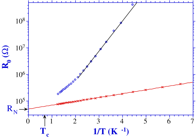
The zero bias resistance was measured as a function of both temperature and magnetic field. All arrays showed an ”insulating” behavior in the N-state, meaning that increased as a function of decreasing temperature. Over a fairly wide range of temperature the dependence was exponential as can be seen in Fig. 7, indicating thermal activation of charge solitons. However, saturates and is no longer temperature dependent at the lowest temperatures, (beyond the range displayed in Fig. 7). This saturation has been discussed in Ref.Delsing-PRB94 and here we will concentrate on the thermal activation.
In the S-state, increased even more rapidly as a function of decreasing temperature for the ”insulating” arrays. The versus curves can be divided into three temperature regions (see Fig. 7). i) In a temperature range below 500 mK, increases exponentially with decreasing temperature, and an activation energy can be defined. ii) At higher temperatures the dependence was not purely exponential due to the temperature dependence of the superconducting gap. iii) For the lowest temperatures became larger than 1 G (not shown in the figure), and could not be measured accurately with our experimental setup.
In a temperature interval roughly between 200 mK and 500 mK, for the ”insulating” arrays could be fitted by a thermal activation dependence over the whole magnetic field range, such that
| (2) |
where is the activation energy and is a constant. It should be noted that there is a region of magnetic field slightly below where the superconducting gap goes to zero in the temperature interval where the fit is made to determine . Therefore, the vs. plots are not perfectly linear at those magnetic fields. However the Arrhenius law (2) is still a fair approximation.
The fact that we do not observe a KTB charge unbinding transition in these arrays is not altogether surprising. It was shown by Zaikin and Panyukov Zaikin/Panyukov-LT21 , that the effect of offset charges will effectively cut of the logarithmic interaction between the charges. Also, the finite size of our samples is probably a limiting factor.
In the N-state, was found to be close to (see Table 1), and b was very close to , for all the ”insulating” arrays. This value of agrees well with that of Tighe et al.Tighe-PRB93 . If the conduction is caused by thermal activation of single electron solitons we expect that in the N-state. The energy required to create a soliton anti-soliton pair starting from an uncharged array, i.e. the tunneling of a single charge, is the so called core energy for single electrons, and four times as high for Cooper-pairs. Similarly to thermal activation in other systems the activation energy becomes half of the core energy.
We next consider the S-state case, where we can imagine two alternative transport mechanisms. On one hand, we can calculate the energy needed to brake up a Cooper pair and to create a SES pair. We would expect and therefore, if the charge transport was entirely due to SESs, created from broken Cooper pairs. If on the other hand, we assume that only CPSs are activated, we would expect the activation energy to be four times higher (because of the 2e charge) than for SESs in the N-state, so that . This picture is of course a bit naive because the Josephson coupling energy is not taken into account. Nevertheless, if this simple picture holds, we would expect that for arrays with , thermal excitation of SESs would always be advantageous, and we would expect . If on the other hand , we would expect a crossover from activation of CPSs to activation of SESs as is suppressed by the magnetic field. All the ”insulating” arrays had , and we thus expect the crossover behavior with magnetic field.
Our observations suggest a somewhat more complicated picture. As we enter the S-state, by lowering the magnetic field below, increases for all the ”insulating” arrays. At zero magnetic field, we find that is equal to or smaller than but larger than , for all seven arrays. In Fig. 8 the magnetic field dependence of is shown for two of the arrays, and it is compared to , which is represented by a dashed line. Here, is measured for each array and the form of the function is also determined from the measurements Delsing-PRB94 .
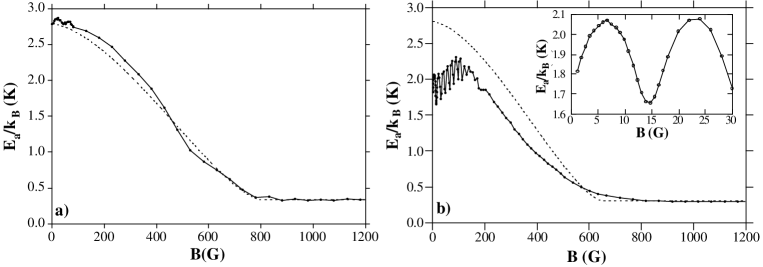
From our simple picture outlined above we would expect the ratio to be important. We find that for arrays with a ratio less than 2, (arrays #12,13, and 15), has a behavior which is very close to , as can be seen for array #13 in Fig. 8a. Arrays #12 and #15 show a very similar behavior. Tighe et al.Tighe-PRB93 have also obtained the same result at for arrays where the ratio was less than 2. However, for the other arrays #9-11, and #14, where was larger than 2, is lower than . This can be seen in Fig. 8b, for array #9. It is obvious that the ratio is important. We find that the critical value is about 2.
In several arrays, we observe oscillations in . The period of oscillation corresponds to one flux quantum per unit cell (see the inset of Fig. 8b). The period agrees very well with the values, determined from geometry. The oscillations show that the Josephson coupling affects the activation energy. The oscillations are observed in all arrays where the measurements were taken with sufficiently small steps of the magnetic field. The amplitude of the oscillations is roughly . Arrays with a large also showed an increase of (the average of) with increasing resulting in a peak at 100 to 200 G (Fig. 8b).
These effects can be understood since the creation of CPS/antiCPS pairs should be dependent on the Josephson coupling. For a weaker Josephson coupling, it should be harder to create CPS/anti-CPS pairs and should increase. The Josephson coupling is affected in two ways by the magnetic field. At low field the cosine part is affected, resulting in an oscillating with maxima where , n being an integer. The oscillations of demonstrate clearly that at least part of the current at low bias is carried by Cooper-pair solitons. At higher magnetic field the increasing with increasing may be explained by a decreasing , and thereby also a decreasing . At even higher fields becomes smaller than 2 so that SES creation dominates, and thus decreases with increasing field
In summary, our results for the N-state agree well with thermal activation behavior, and an activation energy of for single electron solitons can be extracted. For the S-state we find that as long as , pairs of SESs are created by breaking up Cooper pairs so that . For larger values, , pairs of CPSs are responsible for a substantial part of the charge transport and oscillates as a function of temperature.
V The magnetic field tuned superconductor insulator transition
As mentioned previously arrays which are superconducting a low temperature can display a vortex-unbinding KTBKT(B) transition to a resistive state above a certain critical temperature . In zero magnetic field, the theory for KTB vortex-unbinding gives a relation between the superconducting correlation length and the transition temperature . The correlation length is determined by a control parameter which, for example, can be the disorder of the system. A Josephson junction array can be described by the classical 2D-XY model and can be associated to the KTB transition in continuous films LAT . In the presence of disorder, the conductivity at low temperature is governed by variable-range hopping(VRH) Fischer-PRB89 and should scale with . In a highly disordered film, the long-range vortex-pair order is destroyed, and is substantially suppressed compared with that of a disorder-free film. Provided that the transition between insulator and superconductor is continuous, right at a critical disorder, should diverge and should vanish. If the disorder is smaller than but close to the critical disorder, Fisher Fischer-PRL90 predicted, based on the analogy of VRH of vortices to VRH of electrons, that should diverge as ( with exponent , where d=2 is the dimension of the system. The scaling theory developed for the zero field case implies a power law dependence of on , i.e. , with an exponent of unity. Furthermore, the dual transformation suggests a , fixed point where the magnitude of the resistivity (vector sum of the longitudinal and transverse components of the resistivity) should also be universal and equal to .
| # | z | |||||
|---|---|---|---|---|---|---|
| (K) | (k) | () | ||||
| 4 | 1.57 | 0.700.04 | 0.1220.012 | 4.750.5 | 2.450.15 | - |
| 5 | 1.24 | 0.460.04 | 0.0390.007 | 8.201.0 | 1.230.10 | 285 |
| 6 | 0.80 | 0.440.05 | 0.0470.005 | 1.470.2 | 2.200.15 | - |
| 7 | 0.90 | 0.350.04 | 0.0340.010 | 4.450.5 | 1.610.15 | 345 |
Experiments on homogeneous thin films in zero magnetic field demonstrated a SI transition by changing the film thickness. The transition was found to occur when the film sheet resistance was close to a critical value of Haviland-PRL89 . A magnetic field tuned transition was found for films close to the critical resistance Paalanen-PRL92 ; Hebard/Paalanen ; Seidler ; Tanda-PRL92 ; Wu/Adams and agreement with the scaling theory Fischer-PRL90 was obtained. In Josephson junction arrays, a SI transition can be achieved by changing the junction normal state resistance and the junction capacitance CCD-PhysicaScripta ; Fischer-PRL90 . The transition is found to occur near a critical point at RQ and . We therefore expect a magnetic-field-tuned SI transition for arrays near the critical point. However, there is a major difference between a uniform film and a regular array in the presence of an external magnetic field. In the former case the vortices form an Abrikosov (triangular) lattice in the ground state Tinkham-book whereas in the latter case the vortices are pinned in a periodic potential, imposed by the array lattice Halsey . The array lattice results in a ground state energy which is an oscillatory function of the applied magnetic field with period =1 Halsey . The ground state energy is not only periodic, but has minima at rational frustrations, i.e. =1/2, 1/3, 2/3, etc. From one point of view, frustration is simply proportional to magnetic field and should be related to in the scaling theoryFischer-PRL90 . From another point of view, frustration can be consider as introducing defects from the ordered lattice at rational values, in which case the KTB transition under consideration is the melting of the vortex lattice. We thus expect that the value can act as a control parameter for the SI transition, and the scaling theory can be applied, provided one accepts that the correlation length diverges at some critical value of as . Experimentally, we find that the SI transition occurs at =n and n+1/2 (where n is an integer and ), and that the scaling analysis is applicable to both cases.
The important parameters are listed in Table 2. The charging energies were judged from the offset voltage of the -characteristics at large bias. was about 16 G for all the intermediate arrays. For sample #6 the superconducting mean-field-transition temperature, =1.51 K, was measured on an aluminum wire which was fabricated on the same chip as the array. The KTB transition temperature could be deduced from the onset of the linear dependence of CCD-PRB96 , the values are listed in Table 2. This method of deducing has been confirmed both theoretically KT(B) ; Halperin/Nelson and experimentally Hebard/Paalanen ; Martin-PRL89 .
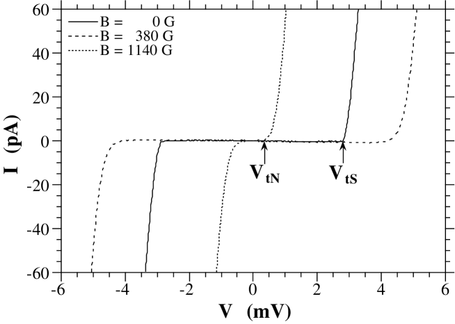
() for sample #4 at is depicted in Fig. 9. Below a critical frustration 0.12, the resistance is lower for lower temperature, indicating a superconducting transition. Above , the resistance is higher for lower temperature, implying an insulating transition. The resistance at , , can be identified from Fig. 9a and is about 2.4 k.
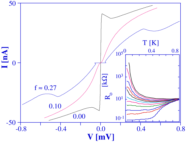
Fig. 9b illustrates the dependence for sample #6 at low temperatures. While arrays #4 and #5 do not show a resistance higher than their normal resistances at any in the accessible temperature range, the resistance of arrays #6 and #7 in the most insulating case (at ) are much greater than their . Remarkably, the resistance of array #6 changes by more than five orders of magnitude going from to at 15 mK. The IV characteristics measured in the superconducting state and in the insulating state for array #6 are displayed in Fig. 10. In the superconducting state, the array exhibits clear Josephson-like current, with 130 , whereas in the insulating state, the array shows an insulating behavior with 0.27) 37 M and a back-bending feature in the IV characteristics similar to the behavior of higher resistance arrays (17 k) reported earlier GeerligsPhysicaB ; CCD-PhysicaScripta . This feature is easily smeared by increasing temperature, resulting in a drastic decrease in the measured in the insulating phase as seen in Fig. 9b. curves for array #6 in the range are shown as an inset of Fig. 10. The flattening-off of the resistance at non-zero frustrations at low temperatures is attributed to a finite size effect, explained within the context of the (vortex) VRH picture Fischer-PRL91 . In this picture, the hopping range increases at low temperature. When the hopping length becomes larger than the sample size, a temperature-independent resistance is expected. This flattening-off behavior was also reported in Refs.vdZant-PRL92 ; Delsing-PRB94 and can be shown to depend on the sample size CCD-PRB96 .
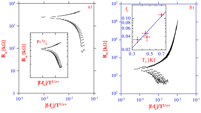
To appreciate the scaling theory, all the data from both the superconducting and the insulating sides should collapse onto a single curve when plotting the resistances against the scaling variable . This is done using both and as free parameters. The curves were determined by minimization of the mean square deviation from an averaged curve on the insulating branch. The scaling was performed in the temperature range 50 mK and in the frustration range . The scaling parameters as well as are listed in Table 1. Scaling curves for arrays #4 and #6 are shown in Fig. 11. All data point in the insulating branch collapse onto the same trend. For the superconductor transition the low temperature points deviate from the general trend due to the finite size effect.
The form of the scaling curves are very similar in the different cases, in fact it is possible to make the curves from all four arrays overlap by offsetting the graphs slightly in the and the direction. The different offsets in the direction demonstrates that the zero temperature fix point is different for the different arrays and that we get sample dependent values of . The offset in the -direction shows an interesting, and unpredicted, linear dependence on the ratio. This is shown in Fig. 12 where is ploted versus the ratio. is the -value at which the superconducting transition extrapolates to zero resistance. Disregarding the low temperature points on the superconducting side, we find that we can describe all the data of the four arrays with a single formula (Eq. 3), where the scaling parameter deduced from theory is normalized to the ratio.
| (3) |
Here F is a universal function describing both the insulating transition and the superconducting transition, and is a nonuniversal, sample dependent parameter.
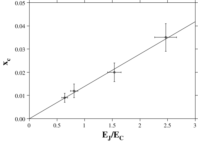
We find, similar to Hebard and Paalanen Hebard/Paalanen , that the quality of the scaling is more sensitive to than to . Using an improper value may cause large discrepancies at the left side of the plot and slightly shift , whereas an improper degrades the scaling but does not change ∗. Note that the scaling analysis is limited to low values by the commensurability between the applied flux and the array lattice. The theory predicts that the transition temperature should scale with the correlation length as . This, together with the fact that depends on the critical frustration as , leads to the relation . Fitting and for the four samples as shown in the inset of Fig. 11b, we can deduce . This can be compared to the theoretically predicted value of unity Fischer-PRL90 .
In the case of =1/2 the region of sample parameters where the phase transition is observable shifts to lower and larger . For array #4 we find , with and is 4.330.15 k. The scaling is shown as an inset in Fig. 11a, the frustration range was . For array B, we find and k. Arrays #6 and #7 have a larger and a smaller ratio, it is thus not surprising that the R curves at various temperatures do not cross near .
Returning to the S-I transition at close to zero, the scaling curves for all four arrays exhibit similar bifurcation shape, but with a different . As other measurements on 2D arrays vdZant-PRL92 ; vdZant-PRB95 and on superconducting films Seidler ; Tanda-PRL92 also showed a different , we conclude that is non-universal and sample dependent. According to theory Fischer-PRL90 the vector sum of the longitudinal resistance (previously ) and the Hall resistance should be universal and equal to RQ at , To check this prediction, we performed measurements of for arrays #5 and #7. Four pairs of Hall voltage probes allow us to check the spread of the junction parameters in an array, which is found to be within 3%. shows a rich structure, the details will be published elsewhere. For both arrays Roxy is of the order of 30 , see Table 2. The sum of and is thus smaller than for both arrays. It should be noted that the smallness of compared with agrees well with recent experiments on thin films Paalanen-PRL92 . The Hall angle at the transition, is about 1.2o for both arrays.
In the thin film case Paalanen-PRL92 a critical field was found also for the data. In our case the linear region in the vs. characteristics is very small at finite , which limits the excitation current and, consequently, the resolution in . Therefore it is hard to determine the crossing point in the ) curves at for both array #5 and #7. Nevertheless, the frustration above which the curves at various T start to deviate from each other seems to be very close to . This is in contrast to the case of disordered films Paalanen-PRL92 where the “critical field“ at which all curves cross is higher than and is associated with the suppression . This is evidently not the case for 2D arrays, since the field needed for suppression of of our arrays is about 800 G Delsing-PRB94 , which is much greater than the critical field (=) of a few G.
VI The Hall effect
Superconducting films can, to some extent, be modeled as a 2D array of Josephson junctions, and understanding their transport behavior can be reduced to the problem of vortex dynamics. Many interesting phenomena occurring in superconducting films can also be seen in 2D Josephson junction arrays. In fact, the phenomena can be more easily modeled in the latter system because complications due to the (often unknown) microstructures do not exist, and phenomenological parameters such as the junction normal state resistance, Josephson coupling energy , and charging energy , can be independently determined. However, there is a major difference between a uniform film and a regular array in the presence of an external magnetic field. In the former case the vortices form an Abrikosov (triangular) lattice in the ground state whereas in the latter case the vortices are pinned in the periodic potential imposed by the array lattice Halsey . The array lattice of loops of area A, results in a ground state energy which is an oscillatory function of the frustration. The ground state energy is not only periodic, but has minima at rational frustrations, i.e. , etc. Halsey . In the vicinity of these rational frustrations, the dynamics is dominated by the motion of ”defect” vortices Rzchowski-PRB94 and the vorticity of the majority defect is reversed upon passing through these rational frustrations.
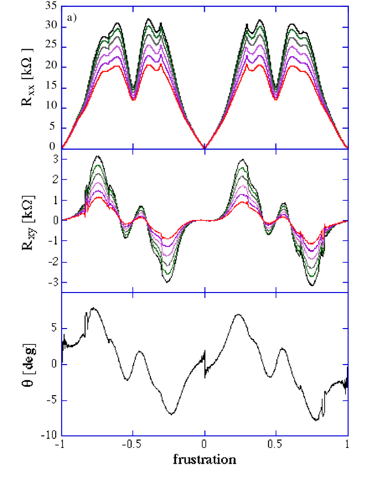
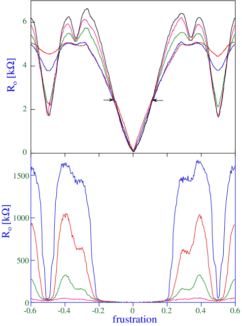
The frustration dependence of and for sample #7 at various temperatures is shown in Fig. 13. is an oscillatory function of the applied magnetic field with period and minima at rational frustrations, and 2/3 as can be seen in Fig. 13. There is a critical frustration, , below which the resistance decreases as the temperature is lowered, and above which the resistance increases as the temperature is lowered. The longitudinal resistance at , k , can be identified from an expanded view of Fig. 13a around , as well from a scaling analysis on these curves which we have discussed in detail in Section V, see also Ref.CCD-PRB95 .
The Hall resistance as a function of frustration is shown in Fig. 13 where we see that it also oscillates with the applied field having the same period . At , is zero, and has a very small negative slope. As the frustration is increased, goes through a minimum, increasing to at . Thereafter it rapidly increases, reaching a maximum value at . As the frustration is increased further, starts to decrease and at , it becomes negative. At , reaches a local minimum and starts to increase to zero at . is anti-symmetric about and locally anti-symmetric about. In the raw data a small symmetric part arises due to sample non-uniformities. This symmetric part can be removed by taking . The removed symmetric part looks identical to, but is only 3% of, . The data shown in Fig. 13 has the symmetric part removed. The difference in shape at and is not understood although it is reproducible for .
The and data can be combined to generate a third plot of the Hall angle which is shown in Fig. 13 at mK. Comparing our results to those of van Wees et al. Wees-PRB87 we find a much larger Hall angle. Furthermore they did not observe an anti-symmetric versus curve. This is probably because their array was in the classical limit , whereas ours were in the quantum limit where a finite has been predicted Fischer-PRL90 ; Otterlo-PRB93
The Hall angle can be interpreted as the angle between the vortex velocity vector . and a unit vector perpendicular to the direction of current flow . The moving vortices generates an electric field given by
| (4) |
with describing the vorticity, the area density of vortices, and the unit vector perpendicular to the plane of the array. Vortex motion in the direction of creates a field parallel to the transport current . The force on a moving vortex is the Magnus force Ao/Thouless-PRL93
| (5) |
where is the superfluid electron density and is the superfluid velocity. Due to this force, there is a component of vortex motion parallel to the applied current which produces a transverse field in the direction.
In two dimensional regular arrays, the field at irrational frustrations is generated by the motion of ”defect” or vacancy vortices. From Eq. 4, it is clear that the sign change in the vorticity is responsible for the sign reversal of in the vicinity of , because the defects have opposite vorticity to the field induced vortices.
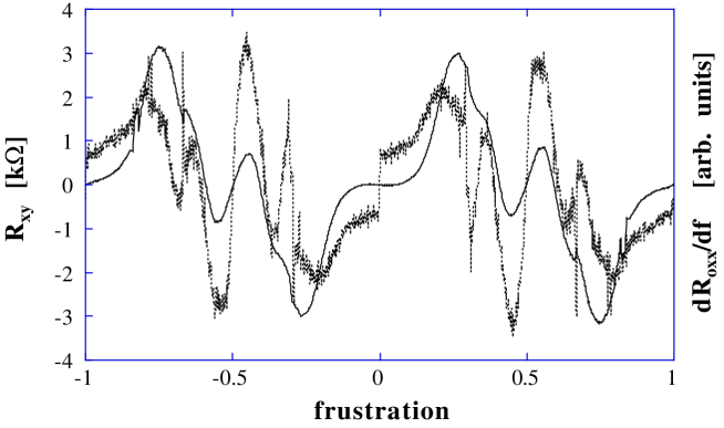
We find that the structures in can be correlated to structure as shown in Fig. 14. The correlation is most clear in the vicinity of . This is similar to what is found in the Quantum Hall effect in two dimensional electron gases (2DEGs), where . That we find traces of the opposite derivative law is probably related to the fact that our system is described in termes of vortices rather than in terms of electrons as the QHE in 2DEGs.
VII Conclusions
Based on the parameters of the tunnel junction we find that we can divide the properties of the 2D arrays into three different categories: i) Those which are dominated by the Coulomb blockade and go insulating at low temperature, ii) those which are dominated by the Josephson effect and go superconducting at low temperature, and iii) the intermediate arrays which just barely become superconducting at low temperature, but can be made insulating by applying a magnetic field.
We find that the transition for the insulating arrays can be well described by thermal activation of charge solitons both when the electrodes are normal and when they are superconducting. When the electrodes are in the normal state we find thermal activation of single electron solitons, with an activation energy . When the electrodes are in the superconducting state we find a much larger . For arrays with , the activation energy is simply indicating that Cooper pairs are broken up and that pairs of single electron solitons are created. When , the activation energy oscillates with at low magnetic field, demonstrating that Cooper pair solitons are created. The amplitude of these oscillations is roughly equal to and the period corresponds to one flux quantum (h/2e) per unit cell.
The threshold voltage for the insulating arrays also oscillates at low magnetic field demonstrating that Cooper pair solitons are injected at low field. For increasing magnetic field the average threshold voltage increases, due to the decreasing . In the region 250 to 450 Gauss we observe a peak in the threshold voltage which is interpreted as a crossover from Cooper pair soliton injection to single electron soliton injection.
We have observed a frustration-tuned superconductor-insulator phase transition in several of the “intermediate” arrays. A small applied magnetic field of 4.4 G can change the zero-bias resistance of an array by more than 5 orders of magnitude. We show scaling curves for both =0 and =1/2. The results for our four samples show a dynamic critical exponent of 1.05, in good agreement with the theory of the field-tuned S-I transition. Our data indicate a sample dependent . Moreover, we have measured the Hall resistance at , which is much smaller than .
For frustration values larger than the critical value the Hall resistance is substantially larger and has a rich structure as a function of applied magnetic field. Reversal of the sign of the Hall resistance appears at several frustrations, which can be attributed to the change of sign of the ”defect” vortices. We find that the structure in is similar to the derivative .
Acknowledgements
We gratefully acknowledge fruitful discussions with S.M. Girvin, M. Jonson, J. E. Mooij, A. A. Odintsov, R. Shekhter, G. Schön, A. Stern, M. Tinkham and H. van der Zant. Our samples were made in the Swedish Nanometer Laboratory. We would also like to acknowledge the financial support from the Swedish SSF, TFR and NFR, and the Wallenberg Foundation.
References
- (1) J.E. Mooij, and G. Schön Single Charge Tunneling, Proc. NATO ASI 294, ed. H. Grabert and M. Devoret, (Plenum, New York, 1992)
- (2) R. Fazio, and G. Schön, Phys. Rev. B43, 5307 (1991)
- (3) N.S. Bakhvalov, G.S. Kazacha, K.K. Likharev, and S.I. Serdyukova, Physica B173, 319 (1991)
- (4) C. B. Whan, J. White, and T. P. Orlando Appl. Phys. Lett. 68, 2996 (1996)
- (5) D.V. Averin, and K.K. Likharev, in Mesoscopic Phenomena in Solids, ed. B. Al’tshuler, P. Lee and R. Webb, (Elsevier, Amst., 1991) p. 173
- (6) Single Charge Tunneling, Coulomb Blockade Phenomena in Nanostructures, ed. H. Grabert and M. Devoret, (Plenum, New York, 1992)
- (7) Percolation Localization, and Superconductivity, Proc. NATO ASI 109, ed. A. M. Goldman and S. A. Wolf (1986)
- (8) Coherence in Superconducting Networks, Proc. NATO ASI, Physica B152 ed. J.E. Mooij, and G. Schön (1988)
- (9) Macroscopic Quantum Phenomena and Coherence in Superconducting Networks, ed. C. Giovannella and M. Tinkham (World Scientific, Singapore, 1995)
- (10) P. Minnhagen Rev. Mod. Phys. 59, 1001 (1987)
- (11) R.F. Voss, and R.A. Webb, Phys. Rev. B25, 3446 (1983)
- (12) C. J. Lobb, D. W. Abraham and M. Tinkham, Phys. Rev. B 27, 150 (1983).
- (13) B.J. van Wees, H. S. J. van der Zant, and J. E. Mooij, Phys. Rev. B35, 7291 (1987)
- (14) T.S. Tighe, A.T. Johnson, and M. Tinkham, Phys. Rev. B44, 10286 (1991)
- (15) H. S. J. van der Zant, F. C. Fritschy, T. P. Orlando and J. E. Mooij, Phys. Rev. B47, 295 (1993)
- (16) M. S. Rzchowski, S. P. Benz, M. Tinkham and C. J. Lobb, Phys. Rev. B42, 2041 (1990)
- (17) C. D. Chen, P. Delsing, D. B. Haviland, Y. Harada and T. Claeson, Phys. Rev. B 54, 9449 (1996).
- (18) J.M. Kosterlitz, and D.J. Thouless, J Phys. C6, 1181 (1973)
- (19) V.L. Berezinskii, Sov. Phys. JEPT 34, 610 (1972)
- (20) J.E. Mooij, B.J. van Wees, L.J. Geerligs, M. Peters, R. Fazio, and G. Schön, Phys. Rev. Lett. 65, 645 (1990)
- (21) L.J. Geerligs, and J.E. Mooij, Physica B152, 212 (1988)
- (22) L.J. Geerligs, M. Peters, L.E.M. de Groot, A. Verbruggen, and J.E. Mooij, Phys. Rev. Lett. 63, 326 (1989)
- (23) C.D. Chen, P. Delsing, D.B. Haviland, and T. Claeson, Phys. Scripta T42, 182 (1992)
- (24) P. Delsing, C.D. Chen, D.B. Haviland, and T. Claeson, in Single-Electron Tunneling and Mesoscopic Devices, ed. H. Koch and H. Lübbig, (Springer, Heidelberg, 1992) p. 137
- (25) T.S. Tighe, M.T. Tuominen, J.M. Hergenrother, and M. Tinkham, Phys. Rev. B47, 1145 (1993)
- (26) P. Delsing, C.D. Chen, D.B. Haviland, Y. Harada, and T. Claeson, Phys. Rev. B50, 3959 (1994)
- (27) A. Kanda and S. Kobayashi Czech. J. Phys. 46, 703 (1996)
- (28) M.V. Feigel’man, S.E. Korshunov, A.B. Pugachev JETP-Lett. 65, 566 (1997)
- (29) H. S. J. van der Zant, F. C. Fritschy, W. J. Elion, L. J. Geerligs and J. E. Mooij, Phys. Rev. Lett. 69, 2971 (1992).
- (30) M. P. A. Fisher, Phys. Rev. Lett. 65, 923 (1990).
- (31) C. Bruder, R. Fazio, A. Kampf, A. van Otterlo and G. Schön, Phys. Scripta T42, 159 (1992)
- (32) P. Lafarge, J. J. Meindersma, J. E. Mooij, Macroscopic Quantum Phenomena and Coherence in Superconducting Networks, (World Scientific, Singapore, 1995) p.94
- (33) A. J. Rimberg, T. R. Ho, C. Kurdak J, Clarke, K. L. Campman and A. C. Gossard, Phys. Rev. Lett. 78, 2632 (1997)
- (34) J. M. Graybeal, J. Luo and W. R. White, Phys. Rev. B49, 12923 (1994)
- (35) A. W. Smith, T. W. Clinton, C. C. Tsuei and C. J. Lobb, Phys. Rev. B49, 12927 (1994)
- (36) A. V. Samoilov, Z. G. Ivanov and L. G. Johansson, Phys. Rev. B49, 3667 (1994)
- (37) J. M. Harris, N. P. Ong and Y. F. Yan, Phys. Rev. Lett. 71, 1455 (1993)
- (38) M. A. Paalanen, A. F. Hebard and R. R. Ruel, Phys. Rev. Lett. 69, 1604 (1992).
- (39) J. Niemeyer PTB Mitteilungen84, 251 (1974)
- (40) G. J. Dolan Appl. Phys. Lett. 31, 337 (1977)
- (41) V. Ambegaokar, and A. Baratoff, Phys. Rev. Lett. 10, 486 (1963), and 11, 104(E) (1963)
- (42) A. Schmid, Phys. Rev. Lett. 51, 1506 (1983)
- (43) Strictly speaking this is not a Schmid Diagram since there one plots the damping term, which is determined by the tunneling resistance. For energies below the gap energy this is different from .
- (44) W. C. Stewart, Appl. Phys. Lett. 12, 277 (1968)
- (45) D. E. MacCumber, J. Appl. Phys. 39, 3113 (1968)
- (46) D. B. Haviland, L. S. Kuzmin, P. Delsing, K. K. Likharev, and T. Claeson, Z. Phys. B85, 339 (1991)
- (47) A. A. Middelton and N. S. Wingreen, Phys. Rev. Lett. 71, 3198 (1993).
- (48) D. B. Haviland and P. Delsing, Phys. Rev. B54, R6857 (1996)
- (49) A. J. Rimberg, T. R. Ho, and Clarke, Phys. Rev. Lett. 74, 4714 (1995)
- (50) A. D. Zaikin and S. V. Panyukov Czech. J. Phys. 46, 629 (1996)
- (51) M. P. A. Fisher, P. B. Weichman, G. Grinstein and D. S. Fisher, Phys. Rev. B 40, 546 (1989).
- (52) D. B. Haviland, Y. Liu and A. M. Goldman, Phys. Rev. Lett. 62, 2180 (1989).
- (53) A. F. Hebard and M. A. Paalanen, Phys. Rev. Lett. 65, 927 (1990).
- (54) H.S.J van der Zant,W.J. Elion, L.J. Geerligs, J.E. Mooij Phys. Rev. B 54, 10081 (1996).
- (55) G. T. Seidler, T. V. Rosenbaum and B. W. Veal, Phys. Rev. B 45, 10162 (1992).
- (56) S. Tanda, S. Ohzeki and T. Nakayama, Phys. Rev. Lett. 69, 530 (1992).
- (57) W. Wu and P.W. Adams Phys. Rev. Lett. 74, 610 (1995).
- (58) M. Tinkham, Introduction to Superconductivity, (McGraw-Hill, New York, 1976)
- (59) T. C. Halsey, Phys. Rev. B 31, 5728 (1985).
- (60) B. I. Halperin and D. R. Nelson, J. Low Temp. Phys. 36, 1165 (1979).
- (61) S. Martin, A. T. Fiory, R. M. Fleming, G. P. Espinosa and A. S. Cooper, Phys. Rev. Lett. 62, 677 (1989).
- (62) M. P. A. Fisher, T. A. Tokuyasu and A. P. Young, Phys. Rev. Lett. 66, 2931 (1991)
- (63) C. D. Chen, P. Delsing, D. B. Haviland, Y. Harada and T. Claeson, Phys. Rev. B 51, 15645 (1995).
- (64) A. van Otterlo, K. H. Wagenblast, R. Fazio, and G. Schön, Phys. Rev. B48, 3316 (1993)
- (65) P. Ao and D. J. Thouless, Phys. Rev. Lett. 70, 2158 (1993)