[
Antiferromagnetic interlayer exchange coupling
across an amorphous
metallic spacer layer
Abstract
By means of magneto-optical Kerr effect we observe for the first time antiferromagnetic coupling between ferromagnetic layers across an amorphous metallic spacer layer. Biquadratic coupling occurs at the transition from a ferromagnetically to an antiferromagnetically coupled region. Scanning tunneling microscopy images of all involved layers are used to extract thickness fluctuations and to verify the amorphous state of the spacer. The observed antiferromagnetic coupling behavior is explained by RKKY interaction taking into account the amorphous structure of the spacer material.
pacs:
75.70.-i,75.70.Cn,75.20.En]
The magnetic exchange coupling between two ferromagnetic layers across a metallic spacer has recently attracted considerable experimental and theoretical interest[2]. Oscillatory exchange coupling with the alignment of the magnetization vectors alternating between parallel (ferromagnetic, FM) and antiparallel (antiferromagnetic, AFM) with increasing spacer thickness was found for most transition-metal[3] and noble-metal [4] and also for some alloy[5] spacers. Theoretically, the oscillating behavior has been explained by the interplay between the Ruderman-Kittel-Kasuya-Yosida (RKKY) interaction and the discrete spacer thickness[6, 7]. Assuming a spherical Fermi surface with Fermi wave number and reducing the RKKY wave number to the first Brillouin zone of the planar periodic structure with a lattice constant , the oscillation period is given by , with . The same relation for can be derived in a picture where the oscillatory exchange interaction with wave length originates from spin-dependent quantum well states in the spacer[8, 9] instead of RKKY interaction. Phenomenologically, the FM and AFM coupling is described by a bilinear energy density term , where is the angle between the magnetizations of the two ferromagnetic layers and the spacer thickness. In addition, a contribution favoring perpendicular arrangement of the magnetizations (90∘ coupling) has been observed[10]. It is parameterized by a biquadratic energy density term, . Several models for the biquadratic coupling have been proposed [11]. Refs. [12, 13] relate this type of coupling to thickness fluctuations of the spacer originating from interface roughness.
Amorphous spacers provide the possibility to study the interlayer coupling in the absence of the structural discreteness which plays a crucial role in all theoretical models proposed so far. A previous study employing amorphous semiconducting spacers[14] revealed AFM coupling with a positive temperature coefficient, which was interpreted as resonant tunneling of polarized electrons through defect-generated localized states in the gap of the semiconducting spacer. Hence, a comparison to the mentioned theoretical models derived for conduction electrons was not possible. Fuchs et al.[15] very recently investigated amorphous metallic AuSn spacers and found FM and 90∘ coupling originating from dipolar interactions while the exchange coupling is strongly suppressed. AFM coupling was not observed. In this Letter we show for the first time that also an amorphous metallic spacer can mediate AFM coupling between ferromagnetic layers and present a model to explain the findings.
Sample preparation and all measurements with the exception of Kerr microscopy are performed in an ultra-high vacuum (UHV) system with a base pressure of 510-11 mbar which is equipped with an -beam deposition system, scanning tunneling microscopy (STM), low-energy electron diffraction, Auger and X-ray photoemission electron spectroscopy (AES, XPS), and a magneto-optical Kerr effect (MOKE) setup. Amorphous metallic CuxZr100-x (-CuZr) is used as spacer material. This alloy vapor-quenches in the amorphous state and stays amorphous at temperatures up to 600 K for the composition used in this work, [16]. We grow the -CuZr spacers by coevaporation from two -beam sources onto substrates held at 490 K. The deposition rates of Cu and Zr are individually controlled by two quartz thickness monitors. Wedge-shaped spacers with a slope of 0.5 nm/mm are grown by linearly moving a shutter in front of the substrate during deposition. The -CuZr spacer is sandwiched by 5 nm thick Fe layers. The bottom one is epitaxially grown in (001) orientation on an Ag(001)/Fe/GaAs(001) substrate following the optimized growth procedures described in Refs. [17, 18]. The top Fe layer is grown at 300 K and adopts a polycrystalline structure. The composition and the cleanness of all layers are confirmed by XPS and AES. For the ex-situ Kerr microscopy analysis the samples are coated with 5 nm Ag and with a ZnS layer for enhancement of the magneto-optical contrast. MOKE-measurements in UHV before and after coating with Ag do not show any effect of the cap layer.
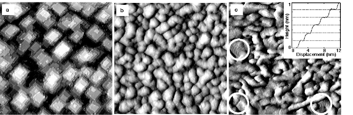
Figure 1a depicts an STM image of the surface of the epitaxial bottom Fe layer. The morphology is characterized by a regular arrangement of equally sized quadratic table mountains. They are delimited by series of single-atomic steps running along axes. The rms-roughness amounts to 0.21 nm. The STM image (Fig. 1b) of the surface of a 2 nm thick -CuZr film, in contrast, shows the typical appearance of an amorphous vapor-quenched thin film: an irregular arrangement of growth hillocks. amounts to 0.44 nm. The weak finestructure consists of nm-sized irregularly arranged features very similar to previously published STM images of sputtered or laser-quenched amorphous ribbons [19]. Our findings are in good agreement with recent STM results of vapor-quenched -ZrAlCu thin films [20]. The STM image of the top Fe layer (Fig. 1c) reveals a grain structure with many single-atomic steps (inset) proving its polycrystalline state.
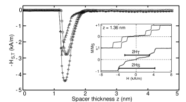
Longitudinal MOKE is used to record magnetization curves. The external field is applied parallel to a easy axis of the bottom Fe layer. A magnetization curve in units of the saturation magnetization taken at nm is shown in the upper part of the inset in Fig. 2. Three plateaus at 0 and 0.5 indicate one phase with vanishing net magnetization and two phases with contribution from only one Fe layer, respectively. AFM coupling at zero field and perpendicular orientation of the magnetizations with one of them parallel to the external field at intermediate field strength is compatible with this magnetization curve. Therefore we call these plateaus AFM and 90∘ plateau, respectively. The small step close to originates from the finite sampling depth of the light and from a weak inequality in thickness or saturation magnetization of the two Fe layers. In order to exclude coercive effects, which could cause a plateau at even in the case of decoupled layers due to different coercive fields, anhysteretic magnetization curves [21] are measured. This is achieved by superimposing to the static external field a decaying AC magnetic field prior to the measurement of each data point of the magnetization curve. The coincidence of forward and backward scan in the lower curve of the inset in Fig. 2 confirms the anhysteretic measurement mode. Obviously, the three plateaus are still visible although their edges are now rounded indicating a more continuous rotation of the magnetizations. The width of the AFM plateau is almost unchanged, whereas the inequality of the width of the 90∘ plateaus has disappeared.
In order to quantify the magnetization curves we define the saturation field and the transition field between the AFM and 90∘ plateaus: () is half the field interval between the values where () averaged over forward and backward scan. Figure 2 shows the dependence of () and () on the spacer thickness . Both show a pronounced peak at nm and vanish for nm. Note that the onset of the peak of is shifted by 0.07 nm towards larger values with respect to onset of at nm. We estimate the total coupling strength as . , where and denote the saturation magnetization and the thickness of the two Fe layers, respectively. Using the Fe bulk value A/m and nm we obtain a maximum coupling strength of -0.05 mJm-2. This value is in the range found for transition-metal and noble-metal spacers[3, 4]. is proportional to the width of the 90∘ plateaus and therefore ( in Fig. 2). It is clearly seen that the biquadratic coupling is strongest at the onset of the AFM coupling.
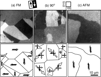
The validity of this interpretation is confirmed by direct domain observation using Kerr microscopy[22]. Figures 3a-c show the domain patterns in the demagnetized, field-free state at three different positions along the wedge corresponding 1.06 nm, 1.15 nm, and 1.25 nm. A domain configuration of FM coupled films with predominantly 90∘ and 180∘ domain walls and the magnetizations oriented parallel to the easy axes of the bottom Fe layer is visible in Fig. 3a. In the transition region (Fig. 3b) all characteristics of 90∘ coupled layers[10, 23] are observed. The straight domain walls are rotated by 45∘ as compared to the FM coupled region separating areas with differently oriented net magnetization (large arrows). Irregularly shaped walls occur between domains with the same net magnetization. Domain observations reveal a width of the transition region of 140 m corresponding to 0.06 nm in good agreement with the shifted onset of compared to in Fig. 2. Figure 3c reveals exclusively irregularly shaped domain walls originating from AFM coupling[10, 23]. For 2 nm the domain pattern indicate weak FM coupling.
The appearance of a single AFM minimum of the coupling at 1.36 nm (Fig. 2) may be explained in terms of RKKY interaction in combination with the oscillatory ion density correlations with wave number in the amorphous spacer. The latter imply that spacer thicknesses of , , are preferred in the deposition process and thus, lead to oscillations of the interlayer coupling with wave number , in analogy to crystalline spacers [6, 7]. However, the rapid decay of the structural correlations in amorphous materials strongly damps these oscillations, so that only the first AFM minimum is observable. In order to quantify this model, we calculate the bilinear coupling energy density between the Fe layers, which is an average over the fluctuating spacer thickness,
| (1) |
Here, is the RKKY coupling between the Fe layers in a planar geometry for a fixed spacing and is the probability for the occurrence of a spacer thickness , when the average thickness is . may be written in terms of the layer correlation function as . is a measure for the spacer thickness fluctuations. Assuming uncorrelated roughness an upper limit for can be calculated from the rms roughnesses of the interfaces, nm. In the planar geometry is the 1-dimensional Fourier transform of the amorphous structure factor .
It has the typical form [24]
| (2) |
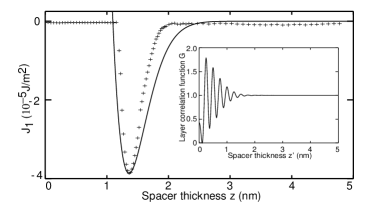
showing a pronounced peak at and approaching a constant value for . We thus obtain the layer correlation function shown in the inset of Fig. 4 exhibiting typical damped oscillatory behavior.
Considering purely bilinear coupling the localized moments in each Fe film are rigidly aligned parallel to each other. Through an exchange coupling , each Fe atom induces an oscillating polarization of the surrounding electron sea , which is transferred to the atoms of the other Fe layer through the paramagnetic spacer. We allow for a phase shift of the RKKY oscillations. In addition, the Fe local moments at the layer surfaces couple directly to the electron states of the -CuZr layer via an exchange coupling . The resulting for a fixed spacing then reads ()
| (3) | |||||
| (4) |
where and are the density of states at the Fermi surface and the Fe lattice constant, respectively, and . The offset arises from the fact that at spacer thickness the Fe layers are still the distance between two Fe lattice planes apart, which is for the Fe bcc structure. The interlayer coupling calculated from Eqs. (1–4) is shown in Fig. 4. Due to the exponential damping, only the first AFM minimum of the oscillations is visible and has a strongly asymmetric shape, in agreement with experiment (+). It is important to note that any phase shift of the microscopic RKKY oscillations would directly appear as a shift of the position of the minimum by . For the present -Cu65Zr35 samples, where and differ substantially, one does not expect a significant phase shift; however such a phase shift should occur when the Nagel–Tauc criterion is satisfied [24, 25]. Our measurements show no indication for . For -Au60Sn40 spacers, which were studied in Ref. [15], and nearly coincide and imply a large oscillation period of 6 nm, rendering the first AFM minimum unmeasurably small. Thus, our model also explains, why no AFM coupling was observed in Ref. [15].
In conclusion, we have measured AFM interlayer coupling across an amorphous metallic spacer exhibiting a single pronounced minimum as a function of the spacer thickness. This result is well explained by RKKY interaction taking into account structural correlations of the amorphous spacer material. It is proposed that the technique presented here provides a direct method to measure a possible phase shift of the microscopic RKKY oscillations predicted in Ref. [25] for amorphous materials.
Financial support from the Swiss National Science Foundation, the Swiss Kommission für Technologietransfer and Innovation and the DFG SP ”Quasikristalle” (J.K.) is gratefully acknowledged.
REFERENCES
- [1] E-mail: buergler@ubaclu.unibas.ch
- [2] For a survey, see e.g. Ultrathin Magnetic Structures, Vol. 2, B. Heinrich and J. A. C. Bland, (Springer, 1994).
- [3] S. S. P. Parkin, Phys. Rev. Lett. 67, 3598 (1991).
- [4] Q. Leng et al., J. Magn. Magn. Mat. 126, 367 (1994).
- [5] P. Bruno, J. Kudrnovský, V. Drchal, and I. Turek, J. Magn. Magn. Mat. 165, 128 (1997).
- [6] R. Coehoorn, Phys. Rev. B 44, 9331 (1991).
- [7] C. Chappert and J. P. Renard, Europhys. Lett. 15, 553 (1991); P. Bruno and C. Chappert, Phys. Rev. Lett. 67, 1602 (1991).
- [8] D. M. Edwards, J. Mathon, R. B. Muniz, and M. S. Phan, Phys. Rev. Lett. 67, 493 (1991).
- [9] J. E. Ortega and F. J. Himpsel, Phys. Rev. Lett. 69, 844 (1992).
- [10] M. Rührig et al., Phys. Stat. Sol. A 125, 635 (1991).
- [11] J. C. Slonczewski, J. of Magn. Magn. Mat. 150, 13 (1995).
- [12] J. C. Slonczewski, Phys. Rev. Lett. 67, 3172 (1991).
- [13] S. Demokritov et al., Phys. Rev. B 49, 720 (1994).
- [14] B. Briner and M. Landolt, Phys. Rev. Lett. 73, 340 (1994).
- [15] P. Fuchs, U. Ramsperger, A. Vaterlaus, and M. Landolt, Phys. Rev. B 55, 12546 (1997).
- [16] A. Regenbrecht, G. von Minnigerode, and K. Samwer, Z. Phys. B 79, 25 (1990).
- [17] D. E. Bürgler et al., Phys. Rev. B 56, 4149 (1997).
- [18] D. E. Bürgler et al., Surface Science 366, 295 (1996).
- [19] T. M. Schaub, D. E. Bürgler, C. M. Schmidt, and H.-J. Güntherodt, J. Non-Cryst. Solids 205-207, 748 (1996); T. M. Schaub, D. E. Bürgler, and H.-J. Güntherodt, Europhys. Lett. 36, 601 (1996).
- [20] B. Reinker, M. Moske, and K. Samwer, Phys. Rev. B 56, 9887 (1997).
- [21] M. Schäfer et al., J. Appl. Phys. 77, 6432 (1995).
- [22] F. Schmidt, W. Rave, and A. Hubert, IEEE Transactions on Magnetics 21, 1596 (1985).
- [23] R. Schäfer, J. of Magn. Magn. Mat. 148, 226 (1995).
- [24] P. Häussler, Phys. Rep. 222, 65 (1992).
- [25] J. Kroha, A. Huck, and T. Kopp, Phys. Rev. Lett. 75, 4278 (1995).