Quantum wires from coupled InAs/GaAs strained quantum dots
Abstract
The electronic structure of an infinite 1D array of vertically coupled InAs/GaAs strained quantum dots is calculated using an eight-band strain-dependent Hamiltonian. The coupled dots form a unique quantum wire structure in which the miniband widths and effective masses are controlled by the distance between the islands, . The miniband structure is calculated as a function of , and it is shown that for the miniband is narrower than the optical phonon energy, while the gap between the first and second minibands is greater than the optical phonon energy. This leads to decreased optical phonon scattering, providing improved quantum wire behavior at high temperatures. These miniband properties are also ideal for Bloch oscillation.
pacs:
73.20.Dx, 73.61.-r, 85.30.VwSemiconductor heterostructures have made possible the construction of low-dimensional electronic systems. By providing confining barriers in one, two, or three dimensions one obtains a quantum well, wire, or dot respectively. It is also possible to increase the dimensionality by coupling a series of low dimensional structures. Here we consider a quantum wire formed by an infinite 1D array of quantum dots. Since the properties of the wire are sensitive to the tunnelling between dots, they may be tuned in a manner that is not possible with other quantum wire structures. Such a structure has been proposed for designing heterostructures with reduced optical phonon coupling.[2]
Periodic arrays of quantum dots have been constructed using stacks of Stranski-Krastanov islands. [3, 4] In Stranski-Krastanov growth a lattice mismatched semiconductor is epitaxially deposited on a substrate material. Due to the mismatch, the deposited material beads up into nm-scale islands, that are subsequently covered with barrier material. If only a small amount of barrier material is deposited over the island, followed immediately by another island deposition, the new islands form directly over the previously deposited islands. By repeating the procedure a series of self-aligned quantum dots is obtained. Since the periodicity is determined by the barrier deposition, it may be accurately controlled.
Photoluminescence experiments on InAs/GaAs island stacks are in rough agreement with estimates using simple 1D models.[4] These estimates were based on repeating the single-band potential from an isolated island, neglecting the strain effects from neighboring islands and band mixing. Also, the full 3D structure were not taken into account. Here we compute the miniband structure employing the full 3D structure, realistic strain, and band mixing.
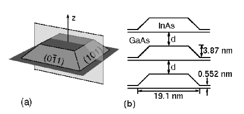
The specific system considered consists of stacked InAs islands embedded in GaAs, as shown in Fig. 1. Each island is a truncated square-based pyramid with -type faces. The islands are wide, high, and include a thick wetting layer. The size and shape are in agreement with transmission electron micrographs, though there is considerable uncertainty in the island geometry. The precise numbers used here come about because the calculation is done on a grid commensurate with the wetting layer thickness. Thus, all dimensions are multiples of the grid spacing, which is fixed by the choice of wetting layer thickness. The islands are assumed to be of fixed size and shape, and only the distance between them is allowed to vary. We consider the range to . The wetting layer is potentially problematic if it is thick enough for the electron wave function to significantly penetrate into the wetting layer. In order to consider the worst case scenario, we assume the wetting layer is thick, which corresponds to two monolayers of InAs biaxially strained to match the GaAs substrate. Most measurements have found the wetting layer to be less than two monolayers thick.
The calculational method has been described in detail elsewhere.[5] Continuum elastic theory is used to compute the strain by discretizing the system on a cubic grid and numerically minimizing the strain energy. The result is used as input to a strain-dependent eight-band envelope-approximation Hamiltonian. The strain induced piezoelectric charge is also included as an additional potential. The Hamiltonian is discretized on the same grid, and its eigenvalues are found by Lanczos diagonalization. An eight-band model is used because InAs has a narrow band gap, making band mixing significant. The narrow gap and large strain result in a near doubling of the electron effective mass within the island[6, 7] which would be neglected in a naive single band approximation. All material parameters are set to the values used in reference 4.


Fig. 2 shows the band structures for and . These were obtained by diagonalizing the Hamiltonian, with and using the local value of the strain. Because the strain extends into the barrier material, the strain within one island is affected by neighboring islands as well. The band diagrams along the direction perpendicular to the wire show good 1D confinement for both electrons and holes. The electrons are confined by a barrier of approximately for , and for . The hole confinement is more sensitive to , varying from to as measured at the center of the island. The band structure along the axis of the wire is shown in Fig 2b. For electrons the on-axis potential varies by about over the range of . Changing primarily alters the electron barrier thickness with little change in the shape of the potential within the island. The valence band is more complex. For small separations the GaAs between the islands is highly strained, resulting in a valence band edge that is higher in the GaAs than in the InAs. This type II behavior is only seen in the potential along the wire axis, and the transverse potential is always confining. For the barrier strain is sufficiently small that the deepest confining hole potential is in the InAs island. The barrier between islands is, however, only about for .


The minimum and maximum miniband energies are plotted in Fig. 3 as a function of island separation. The conduction band states are the most interesting since they have the largest subband spacings. The minima and maxima are at and respectively, where is the momentum along the wire, and is the period. For the first miniband separates from the other minibands, although the second and third minibands still overlap since they are nearly degenerate. (The small splitting is due to the piezoelectric charge that breaks the symmetry of the square island down to .[5, 8] ) The most interesting regime is , where the gap between the first and second minibands is greater than , and the width of the first miniband is less than . Since the optical phonon energy is approximately , both interband and intraband transitions will be suppressed; an electron in the lowest miniband has no final states available one optical phonon energy away. Since optical phonon scattering is dominant at high temperatures, the structure described here should maintain quantum wire behavior to higher temperatures than ordinary wires.
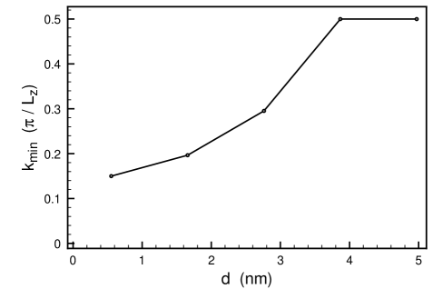
In contrast to the conduction band, the valence band structure is considerably more complex (Fig. 3b). The miniband spacings range from to while the miniband widths vary from to less than . For the three highest valence minibands are non-overlapping, while for there are no gaps. At large values of the miniband widths are sufficiently small to suppress optical phonon scattering, however the gaps between minibands are too small to suppress interminiband scattering. The valence miniband minima all occur at and the maxima occur away from zone center. Such indirect gaps are also seen in standard quantum wires.[9] Fig. 4 shows the value of for which is a maximum, as a function of . For the miniband maximum occurs at the minizone edge, while for smaller separations the maximum occurs in the middle of the zone.

While the miniband widths determine the quantum wire properties of the structure, they are not directly measurable. A quantity such as the miniband gap is useful for characterizing the structure since it may be measured using photoluminescence. Fig. 5 shows the miniband gap as a function of island separation. For simple coupled quantum dots one expects a minimum energy at , monotonically increasing with . However, due to the fact that affects the strain, the gap turns over, giving a maximum gap at . Photoluminescence measurements give for stacks containing up to 10 islands and with .[4] The gap shown in Fig. 5 is somewhat smaller ( ), however this slight difference is not significant given the uncertainties in the island size.
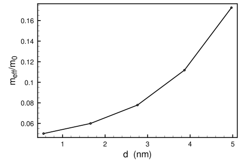
The miniband structure may also be parameterized by the effective mass, which was calculated for the first conduction miniband by fitting a parabola to around (Fig 6). For contiguous islands , which is comparable to the value calculated within a single InAs islands.[6, 7] With increasing barrier thickness the effective mass increases quickly, reflecting the exponentially suppressed tunnelling probability. This ability to tune the effective mass allows a degree of band engineering not available with standard wire structures.
The quantum wire structure described above is particularly well suited to producing Bloch oscillations.[10] Bloch oscillations have been measured in superlattices, however, due to dephasing effects the oscillations are heavily damped and only a few periods are observed. The wire structure presented here lacks the transverse excitations present in superlattice structures, eliminating this source of damping. At low carrier densities the damping has been attributed to optical phonon scattering[11]. Thus island stacks with should make improved Bloch oscillators. Damping is also produced by imperfections in the periodicity[12], which of course island stacks also suffer from due to growth variations.
In conclusion, we have seen that quantum wires with non-overlapping minibands may be obtained from vertically coupled strained InAs/GaAs quantum dots. For an island spacing the lowest electron miniband width is less than the optical phonon energy, and the gap to the second miniband is greater than the optical phonon energy. This results in quantum wires with decreased optical phonon coupling. The same range, , gives a miniband structure favorable for generating Bloch oscillations.
I wish to thank Mark Miller for stimulating discussions.
REFERENCES
- [1] e-mail: cpryor@mail.igalaxy.net
- [2] H. Sakaki, Jpn. J. Appl. Phys., 28, L314 (1989).
- [3] Q. Xie, A. Madhukar, P. Chen, and N. P. Kobayashi, Phys. Rev. Lett. 75, 2542 (1995); G. S. Solomon, M. C. Larson, and J. S. Harris, Appl. Phys. Lett. 69, 1897 (1996); M. S. Miller et al, J. Appl. Phys., 80, 3360 (1996); M. S. Miller, Jpn. J. Appl. Phys. 36, 4123 (1997).
- [4] G. S. Solomon, J. A. Trezza, A. F. Marshall, and J. S. Harris, Phys. Rev. Lett. 76, 952 (1996); M. S. Miller S. Jeppeson, and L. Samuelson, Superlatt. and Microstruct. 23, 34, 45 (1996).
- [5] C. Pryor, M-E. Pistol, L. Samuelson, Phys. Rev. B 56, 10404 (1997).(also at http://xxx.lanl.gov/abs/cond-mat/9705291)
- [6] M. A. Cusack, P. R. Briddon, and M. Jaros, Phys. Rev. B 54, 39 (1996).
- [7] C. Pryor, http://xxx.lanl.gov/abs/cond-mat/9710304.
- [8] M. Grundmann, O. Stier, and D. Bimberg, Phys. Rev. B 52, 11969 (1995).
- [9] P. C. Sercel, K. J. Vahala, Phys. Rev. B, 42, 3690 (1990).
- [10] For a review on Bloch oscillations see F. Rossi, http://xxx.lanl.gov/abs/cond-mat/9711188.
- [11] F. Rossi et al, Phys. Rev. B, 51, 16943 (1995).
- [12] J. P. Reynolds, M. Luban, Phys. Rev. B, 54, R14301, (1996).