[
Prediction of a New Type of Strain Induced Conduction Band Minimum in Embedded Quantum Dots
Abstract
Free standing InP quantum dots have previously been theoretically and experimentally shown to have a direct band gap across a large range of experimentally accessible sizes. We demonstrate that when these dots are embedded coherently within a GaP barrier material, the effects of quantum confinement in conjunction with coherent strain suggest there will be a critical diameter of dot (60Å ), above which the dot is direct, type I, and below which it is indirect, type II. However, the strain in the system acts to produce another conduction state with an even lower energy, in which electrons are localized in small pockets at the interface between the InP dot and the GaP barrier. Since this conduction state is GaP -derived and the highest occupied valence state is InP, -derived, the fundamental transition is predicted to be indirect in both real and reciprocal space (“type II”) for all dot sizes. This effect is peculiar to the strained dot, and is absent in the free-standing dot.
pacs:
PACS:73.20.-r, 73.20.Dx, 85.30.Vw]
There are two leading techniques for fabricating InP quantum dots; (i) colloidal growth, producing unstrained, chemically passivated dots[1] and (ii) dots grown by the Stranski-Krastanov mechanism that are embedded within a semiconductor barrier such as GaInP[2, 3]. In a recent study of the electronic structure of colloidally grown InP dots[4] it was found that these dots have a direct band gap at the -point of the Brillouin zone for all experimentally accessible sizes. In contrast, it has previously been shown that for free-standing GaAs dots, the band gaps can undergo a transition from direct to indirect as a result of quantum size effects[5]. The effects of quantum confinement are that as one decreases the size of the dot, all of the conduction levels are pushed up in energy at a rate reflecting approximately the inverse of the electron effective mass. Since the masses are generally lighter than masses[6], reduced sizes can transform a direct dot into an indirect dot if the initial - separation in the bulk is not too large. It has been predicted[7] that in GaAs, where the bulk - separation is only 0.55 eV[6], a free-standing, zero-pressure dot will become indirect at a dot size of 40Å , whereas an AlAs-embedded GaAs dot will become indirect at 80Å [7]. Since, however, in InP the - bulk separation is large (0.94 eV[6]), calculations[4] have predicted that this separation is not overcome by quantum-size effects, and free-standing dots will remain direct at all sizes at zero pressure.
In this paper we are interested in investigating whether InP quantum dots embedded within a GaP matrix exhibit a direct-to-indirect transition as a function of size and thereby exhibit significantly different electronic structure to free standing InP quantum dots that are direct for all sizes. We find indeed that for spherical InP dots smaller than 60Å in diameter, the conduction band of the unstrained GaP barrier is lower than the -state of the InP. This is analogous to a “type II in real-space and in reciprocal space” state familiar[8] in AlAs/GaAs nanostructures. Surprisingly, however, we find that under the influence of the hydrostatic and biaxial strain present at the GaP/InP interface, a new conduction state emerges that is lower in energy than both the unstrained bulk GaP -state and the InP -state. This qualitatively new type of state is localized at the interface of the dot and its barrier, and is indirect (-like). Hence, when coherency exists between InP and GaP, we predict that photo-excited electrons will be localized in this state, giving rise to an unusual dependence of the band gap on size. This effect is peculiar to coherently strained systems, and is absent in free-standing (colloidal) dots.
Expected trends based on band offsets: Before presenting our calculated results for GaP-embedded InP dots, we discuss the basic expectations regarding the nature of the confined states. Figure 1a shows our fitted[9] unstrained (“natural”) valence and conduction band offsets between bulk InP and bulk GaP. The states are shown as heavy solid lines and the states as thin solid lines. We see that InP can act as a “well” both for the conduction band electrons and the valence band holes (a “type I” offset). The confined levels are denoted schematically by dashed lines. As the InP dot becomes smaller, quantum confinement causes the confined InP valence levels to be pushed down in energy and the confined conduction levels to be pushed up (see arrows). This causes the -level to be pushed up in energy with respect to the -level in the GaP barrier causing a direct-to-indirect transition (see below).
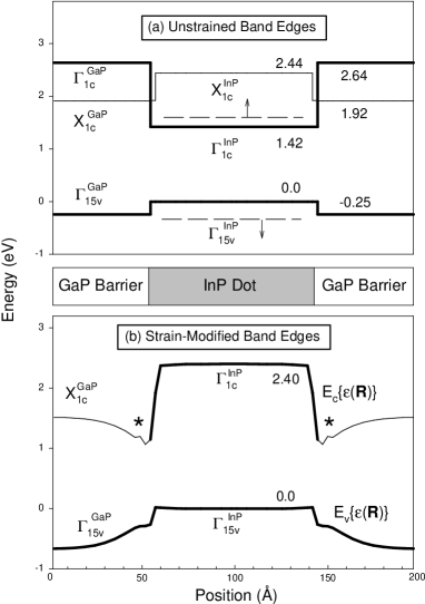
In reality, the large (7%) atomic size-mismatch between GaP and InP will cause atoms to be displaced off their ideal zincblende positions. This will alter the effective band offsets of Fig 1a and thus the anticipated confinements. To calculate the ensuing strain we place an InP sphere of radius R inside a large GaP cube, and relax all the atomic positions to their minimum strain energy values, using the Valence Force Field (VFF) elastic energy functional[10]. We chose to fix the external dimension of the GaP cube during the relaxation as this most closely resembles the experimental situation where InP dots are grown[2] on a fixed GaP substrate and the dot-dot separation is large enough to remove any dot-dot interactions. However, in the systems studied here, the large barrier sizes create such a high GaP:InP ratio ( 30:1) that any external relaxation would be minimal in any case. The resulting strain exhibits nontrivial hydrostatic and biaxial components. Our quantum mechanical calculation of the energy levels of the dot (see below) will include the effect of such a strain profile. However, in order to understand these results, we first consider a simpler case, namely we calculate the band edge states of bulk InP and bulk GaP subject to the local strain, , experienced by the GaP embedded InP dot at position . To do this we discretize the GaP/InP nanostructure into “cells” with position vector R and then perform 40 bulk band structure calculations of InP and GaP, using the empirical pseudopotential method[11], thus obtaining the bulk eigenvalues for band at wavevector within each cell. Each bulk calculation, , uses the In-P or Ga-P bond geometry within that cell. The resulting strain-modified band edge states are shown in Fig. 1b. Compared with the unstrained offsets (Fig. 1a), we see that the GaP -band edge that is flat in the absence of strain (Fig. 1a) is now transformed into an attractive trough (indicated by * in Fig. 1b), capable of localizing electrons. The formation of this trough is initially surprising as the deformation potential at the -point is positive and one might therefore expect the hydrostatic expansion of the GaP at the interface with the InP dot to drive the -state up in energy. However, the above bulk calculations show that it is the biaxial strain present at this interface which is the dominant term, and this is capable of forming the electron troughs. The atomistic strain has therefore profoundly modified the nature of the confined electron states from delocalized to localized. It is important to emphasize that conventional[12] calculations of strain modified conduction band offsets include only the hydrostatic (no biaxial) term and only the (no ) conduction band, and would therefore miss the important changes in the conduction band edges between Figs. 1a and 1b which our calculations show are due to the effect of biaxial deformation on the state.
Results of calculations on dots: To calculate the energy levels of GaP embedded InP dots, we again place an InP dot of radius R, surrounded by sufficiently thick GaP barrier in a “supercell”, repeated periodically to create a lattice of dots. Having created (artificial) translational periodicity, band theoretical methods can then be applied to study the electronic properties. The limit of an isolated dot is achieved by increasing the thickness of the GaP barrier. The calculations for both the bulk bands and the quantum dot levels are based on the atomistic Hamiltonian
| (1) |
The total potential is constructed from screened atomic pseudopotentials, , where represents Ga, In and P, and are the relaxed atomic positions. The pseudopotentials, , have been fitted[9] to the experimental band gaps, deformation potentials and effective masses. We use the analytic form of the pseudopotential described in Ref.[9], which was designed to build in the effects of strain experienced by each atom in lattice mismatched systems.
The supercells studied in this paper contain up to one million atoms, which is too large for the Hamiltonian in Eq.(1) to be solved by direct diagonalization. We thus use the “Folded Spectrum Method” (FSM) [13, 14], in which one solves for the eigenstates of the equation
| (2) |
where is a reference energy, and the wavefunctions, , are expanded in a plane wave basis. By placing within the gap, and close to the valence band maximum or conduction band minimum, one is then able to obtain the top few valence states or the bottom few conduction states respectively. Using this approach the computational cost scales as , where is the number of desired electronic states and is the number of plane wave basis functions ( million in the largest system studied here). The simulations in this paper were performed using a parallel code on the Cray T3E900 on up to 256 processors where the ellipsoid of -vectors is divided over the processors in a similar way to the method used by Clarke et al[16]. Using this data distribution and fast parallel FFT’s, almost linear speed up with the number of processors can be obtained for the large systems studied.
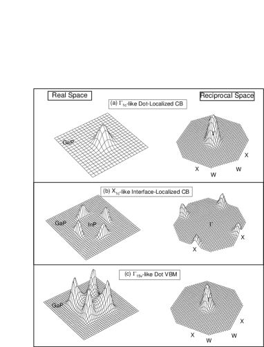
To facilitate comparison with the spherical free standing InP quantum dots studied in Refs.[4], we constructed a series of supercells containing spherical InP quantum dots with diameters of 44, 87, 131 and 174 Å. Each dot was surrounded with sufficient GaP barrier material to produce dot-dot separations of 109, 152, 196 and 239 Å respectively. The calculated energies of the highest occupied valence states and lowest empty conduction states are shown in Fig. 2. The left hand side of Fig. 3 illustrates the corresponding wavefunctions squared of the 131 Å dot. We see that the highest energy valence wavefunction is localized within the InP dot (Fig. 3c), whereas the lowest conduction wavefunction is localized in pockets at the {001} facets of the interface between the InP dot and the GaP barrier (Fig. 3b). The energy of this interfacial state is considerably lower than the unstrained bulk GaP -state (solid line in Fig.2) for all the dots studied. To establish the identity of these wavefunctions in terms of the parent GaP and InP bulk states, we project the dot wavefunctions, , into the zincblende Brillouin zone using the method described in Ref.[15]. This mapping is shown on the right hand side of Fig. 3 for the plane through the Brillouin zone. We see that the highest energy valence state is a -derived state (Fig. 3c), while the lowest conduction state is -derived (Fig. 3b). The calculated dipole transition matrix element between these states is 5 orders of magnitude smaller than one would expect between a more typical pair of -derived conduction and valence states, rendering the transition forbidden.

To investigate the effect of dot-dot separation, a series of similar calculations were performed on the quantum dot with a diameter of 87 Å, where the dot-dot separation was steadily increased to values of 152, 196 and 240 Å. The energies of the -derived, interface localized states were -4.15, -4.22 and -4.22 eV respectively. The invariance of this state with dot-dot separation strongly suggests that the strain induced interface localization evident in Fig 3b is not due to too small a choice of supercell, but an intrinsic effect present at such a interface. Given that the lowest-energy conduction state, as illustrated in Fig. 3b is an -derived, interfacial state, one wonders where is the -derived dot conduction state. It would not be practical to use the FSM to search for this state as the large size of the supercell folds many eigenstates to the -point (at which the FSM calculation is performed) between the lowest conduction state and the -derived state. We instead use the Linear Combination of Bulk Bands (LCBB)[17] method which specifically searches for states of a given symmetry (e.g. -derived), whether or not they are the lowest energy. Here one first solves for a set of bulk Bloch wavefunctions, , of the two materials, InP and GaP. Then the Hamiltonian from Eq.(1) is diagonalized within the basis of these wavefunctions. The LCBB method allows one to choose which bulk Bloch wavefunctions to include in the basis set. As we are only interested here in the -derived energy levels, we include bulk Bloch wavefunctions from a radius of (in reciprocal space) around the -point, where is the supercell length. The resulting eigenstates were found to be converged with respect to the basis size at this radius. The wavefunction squared of the -derived state for a system containing a dot with a diameter of 131 Å is plotted in Fig. 3a. The energies of the -derived states in each of the four InP quantum dots are shown in Fig. 2. Figure. 2 shows that there is a critical dot diameter around 60 Å below which the -derived conduction state in the InP quantum dot is higher in energy than the bulk -state of the GaP barrier. This is a type I to type II transition. However, for all sizes of InP dot, the -derived state is higher in energy than the -like interfacial state.
In conclusion, we have shown that: (i) the effects of quantum confinement and pressure raise the energy of the -derived state in an InP quantum dot so that for dots smaller than 50Å, this state is higher than the state of the unstrained GaP barrier. This transition is analogous to the AlAs-embedded GaAs dot, where the CBM moves from GaAs- to AlAs- as the GaAs size decreases. However, (ii) strain induces an even lower energy state, indirect in reciprocal space and localized in real space at the interface between the InP dot and the GaP barrier. Therefore, we predict that, even for large, spherical InP dots, as long as coherency is maintained, the effects of strain create a system with an indirect band gap, that is considerably reduced due to the low lying interfacial state. This is in direct contrast to the the behavior of free standing InP dots, which are direct over the large range of experimentally accessible sizes.
Acknowledgements This work was supported by United States Department of Energy – Basic Energy Sciences, Division of Materials Science under contract No. DE-AC36-83CH10093. The calculations were performed using the Cray T3E, located at the National Energy Research Scientific Computing Center, which is supported by the Office of Energy Research of the U.S. Department of Energy.
REFERENCES
- [1] O. Micic, C. Curtis, K. Jones, J. Sprague, and A. Nozik. J. Phys. Chem. 98, 4966 (1994)
- [2] N. Carlsson, W. Seifert, A. Petersson, P. Castrillo, M. Pistol, and L. Samuelson. Appl. Phys. Lett 66, 3093 (1994)
- [3] C. Ulrich, S. Ves, A. Goni, A. Kurtenbach, K. Syassen, and K. Eberl. Phys. Rev. B 52, 12212 (1995)
- [4] H. Fu and A. Zunger. Phys. Rev. B 55, 1642 (1997) ; ibid 56, 1496 (1997)
- [5] A. Franceshetti and A. Zunger. Appl. Phys. Lett. 68, 3455 (1996)
- [6] Landolt and Bornstein. Volume 22, Sub-volume a, edited by O. Madelung. Springer-Verlag, (1997)
- [7] A. Franceshetti, S.-H. Wei, and A. Zunger. Phys. Rev. B, Rapid Commun. 50, 8094 (1994)
- [8] G. Li, D. Jiang, Z. Wang, and K. Ploog. Phys. Rev. B 40, 10430 (1989)
- [9] J. Kim, A. Williamson, L. Wang, S.-H. Wei, and A. Zunger. submitted to Phys. Rev. B
- [10] P. Keating. Phys. Rev. 145, 637 (1966)
- [11] J. Chelikowsky and M. Cohen. Phys. Rev. B 14, 556 (1976)
- [12] M. Cusak, P. Briddon, and M. Jaros. Phys. Rev. B 54, 2300 (1996)
- [13] L.W. Wang and A. Zunger. J. Chem. Phys. 100, 2394 (1994)
- [14] L.W. Wang and A. Zunger. Semiconductor Nanoclusters, edited by P.V. Kamat and D. Meisel Elsevier Science, (1996)
- [15] L.W. Wang and A. Zunger. Phys. Rev¿ B 56 (1997)
- [16] L.J. Clarke, I. Štich and M.C. Payne. Computer Physics Comms. 72, 14 (1992)
- [17] L.W. Wang, A. Franceshetti, and A. Zunger. Phys. Rev. Lett. 78, 2819 (1997)