Conductivity and Atomic Structure of Isolated Multiwalled Carbon Nanotubes
Carbon nanotubes discovered by Iijima [1] are quite unusual objects which, apparently, have no analogs in the solid state. According to theoretical predictions [2], a single graphite layer wrapped into a cylinder, can be a metal or a semiconductor depending on its diameter and helicity. Due to the peculiarity of the Fermi surface of 2D Graphite which is reduced to a set of discrete points [3], there are only two conducting channels in a shell independently of its diameter. Thus, single walled nanotubes (SWNT), constitute in principle ideal candidates for the study of electronic transport at 1D. However they are difficult to isolate and manipulate for transport properties. The experiment by Tans et al. [4] showing evidence of single electron tunneling in an isolated single-wall nanotube deposited on a silicon substrate is a first fundamental step in this direction. However the non metallic character of the electrical contacts in that experiment did not allow direct investigation of transport. On the other hand multiwalled nanotubes [5] are easier to manipulate. Electron microscopy investigations show that they generally consist of shells of different helicity. That is, such a nanotube is a solid body in which one atomic layer can be a metal and another a semiconductor. Transport measurements started in 1995, when some of us succeeded in measuring the conductivity of an individual nanotube [6]. Then, several works on this problem were quickly reported [7, 8, 9]. In particular Ebessen et al.[9] have systematically studied the electrical properties of a large number of nanotubes. It was found that ”each multishell nanotube has unique conductivity properties”. The authors also suggested that the difference in electric properties is due to the difference of the nanotubes structure. However, even the inner diameter or the number of shells in these nanotubes were unknown (this is also pertinent to works described in [7, 8]). It seemed obvious that a detailed investigation of the nanotubes structure would contribute to the understanding of nanotubes electric properties.
In this letter, we report the results of simultaneous investigations of the electric properties and structure of nanotubes in the transmission electron microscope. The technique used for isolating an individual nanotube is qualitatively different from the other studies [7, 8, 9]. It allows studying in HRTEM the structure of the nanotube. The method consists in the following: a focused laser beam ”shakes off” a nanotube from the target onto a sample with a membrane covered with a metal film [10, 11]. A submicron width slit about in length has previously been cut in the membrane by focused ion beam; the nanotube connects the edges of the slit see fig.1 and shorts the electric circuit whose resistance was over before the nanotube was ”shaken off”. In the following we successively discuss electron microscopy observations and transport measurements on a family of tubes indexed as , , depending on the nature of the used metal contact.
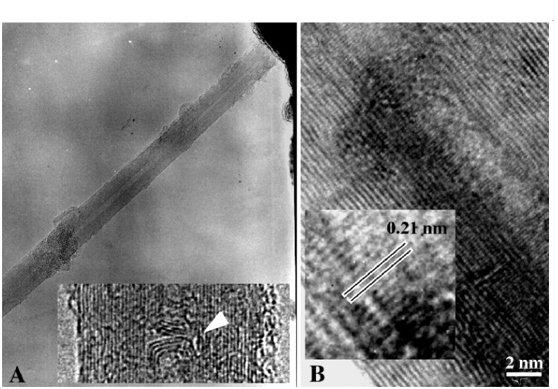
The high resolution electron microscope (HRTEM) is a powerful tool to visualize the atom arrangement in solids. In the case of carbon nanotubes, the observed contrast can easily be related to the graphitic structure. Graphite layers ((002) lattice planes), when parallel to the electron beam i.e. in the Bragg diffraction conditions, are seen as black and white fringes corresponding to the projection of atomic positions. A carbon nanotube is therefore seen as a set of fringes parallel to the tube axis, generated by the sectors of the coaxial curved graphite sheets which lie parallel to the beam. Like in graphite, the distance between the layers is approximately 3.4 Å. We have used such pictures to estimate the inner and external tube diameters and the number of layers composing the nanotube. The structural parameters concerning the whole set of investigated individual tubes are listed in table 1. We have also confirmed that the metal from the contact does not wet the internal hollow of the nanotube.
| Sample | # of | L | Bamboo | R | R | Type | |
|---|---|---|---|---|---|---|---|
| name | (nm) | shells | () | defects | 100K | ||
| 25 , 7 | 26 | 2.1 | No | ||||
| 40 , 3 | 55 | 0.33 | No | ||||
| 25 , 5 | 29 | 0.45 | Yes | ||||
| 16 , 5 | 16 | 0.36 | Yes | ||||
| 7 , 2 | 7 | 0.35 | Yes | ||||
| 13 , 7 | 9 | 0.17 | Yes | ||||
| 12 , 4 | 11 | 0.4 | Yes | 2 | |||
| 25 , 3 | 29 | 0.17 | No | 2 | |||
| 26 , 5 | 31 | 0.33 | No | 2 |
Another structural parameter is the helicity of the layers, i.e. the way the carbon hexagons paving the graphite sheet are oriented with respect to the tube axis. In non helical tubes, the hexagons in two sectors diametrically opposed are parallel. As a result of the hexagonal lattice symmetry, the contrast in the areas with graphite planes perpendicular to the electron beam is composed of 3 families of parallel fringes arranged in a three fold symmetry pattern. The distance between these fringes is 2.1 Å and one family of fringes is either perpendicular to the tube axis (zig-zag tubes) or parallel to the tube axis (arm-chair tubes). As an example, we show in fig.1B a high resolution image of the tube constituting Sn2 sample. In this case, one family of fringes is more obvious than both others. The fringes are perpendicular to the tube axis indicating that the cylinders configuration is zig-zag like. This picture according to simulations by Zhang et al. [12] is a strong indication for a graphite like stacking of most of the the nanotube shells. Most investigated nanotubes cannot be described only as perfect sets of coaxial cylinders, but exhibit defects which can affect the transport mechanisms. In particular a defect so called bamboo defect in the literature [13], has been identified in many cases: the inner shells of the nanotube are interrupted and separated by fullerenic semi-spheres while the outer shells remain continuous, (see fig.1A). The presence of such defects is indicated in table 1. We will see that the presence of these defects affects transport properties when there exists a possibility of conduction between the outer and inner shells of the tube.

Concerning transport properties two main types of behavior have been observed: semi-conducting, (type , ) and quasi-metallic, (type) as depicted below:
Most samples belong to type . They exhibit a semi-conducting behavior below , with exponentially activated temperature dependence of the resistance,(see fig.2). Typical gaps values lie between 2000 and 3000 K, similar to values obtained in amorphous graphite [14]. Note however, that the room temperature values of the effective resistivities, estimated from length and section of the tubes , are all below which is orders of magnitude smaller than the typical values obtained for amorphous graphite. For some of these tubes (type), a saturation of the resistance around is observed below 100K. It is striking that all these tubes contain one ”bamboo” defect. These samples are also characterized by their strongly non linear characteristics below , see fig.3. In most cases the curves are not symmetrical in and also exhibit hysteresis and telegraphic noise only for one particular voltage sign. The typical voltage scale for the non-linear behavior is of the order of few tenths of volts. At 4.2K and below the differential conductance exhibits some narrow peaks characteristic of a Coulomb blockade stair-case like behavior (width of the order of 10mV). For particular voltage values, telegraphic noise could also be recorded. The characteristic time scales are of the order of the ms at 77K and 1000s below 1K.
A few tubes (Au4, Au3 and Bi5) belong to type and exhibit a ”quasi-metallic” behavior. Their resistances increase more slowly than exponentially at low temperature, varying approximatively like (see fig.2 with for Au3 and for Au4, a lower increase was observed for Bi5. We never see any increase of resistance at high temperature similar to what is observed in ”bulk” samples of SWNT [15]. Note however that this type of true ”metallic” behavior has only been recorded so far in ”bulk” samples or ropes of SWNT and has never been reported for isolated nanotubes. On the Au3 sample we could also perform very low temperature transport measurements, shown in fig.4. The curve exhibits a broad maximum around 0.6 K. The amplitude and position of this maximum varies drastically with the magnitude of magnetic field applied perpendicularly to the tube axis. It shifts to lower temperature with increasing magnetic field and reaches higher resistance values. Accordingly, one observes a large positive magneto-resistance approximatively linear in magnetic field (with a increase for an applied field of 4T.) To our knowledge it is the first time that such remarkable features have been observed in the resistance measurements of nanotubes. These findings are in contrast with those of Langer et al. [7] who had measured negative magnetoresistance, which could be interpreted as a weak localization effect.
One important issue for understanding transport properties of these nanotubes is the separation between the contribution of the most external shell, which is the only one directly connected to the metallic pads, and the possible contributions of internal shells. This is determined by the ratio between the resistance of this external shell and the resistance connecting this shell to internal shells. The combination of HRTEM observations and transport measurements suggests that for type and type nanotubes. One convincing example is the Sn2 sample: it contains 60 shells which, according to HRTEM observations, are arranged for most of them in a nearly perfect metallic graphite type of order. However the temperature dependence of its resistance indicates a semiconducting behavior. These two results can be reconciled if transport takes place in the external shell of the tube and if there is no possibility of conduction through internal metallic shells. Unfortunately, we do not have any indication whether semiconducting behavior is related to the helical structure of the tube external shell or to structural disorder in this shell.

The situation is different for type samples, where figures 2 and 3 indicate a residual tunneling conductivity at low temperature. A possible explanation of these findings could be tunneling on a metallic inner shell of the tube, behaving as a Coulomb island, separated from the metallic pads by external shells which are insulating at low temperature but however offer the possibility of electron transfer through high but finite tunneling resistance . HRTEM observations reveal a complex situation with the existence of ”bamboo” like defects It is more reasonable to assume that these nanotubes contain 2 distinct metallic islands and eventually 3 tunnel junctions. The capacitance of such junctions of typically dimensions is of the order of . On the other hand the capacitance of a metallic layer of length and diameter is of the order of . It corresponds to charging energies of respectively and , i.e. which are compatible with the voltage scales of the features observed in fig.3 on the non linear characteristics of these systems. The existence of telegraphic noise is related to the great sensitivity of the conductance of these junctions to structural defects which are still mobile at low temperature for specific values of dc polarization of the sample. Note also that the hysteresis in these curves observed only for positive values of voltages cannot be of thermal origin and may be due to some electro-mechanical effect. We finally note that bamboo defects are only relevant for these type tubes for which internal shells play an important role in low temperature transport properties (). They also exist in some type and type samples but we do not think that they affect their transport properties which are mainly determined by the outer shell ().

Concerning type 2 samples, it is interesting to compare our results with the power-law increase of the low temperature resistance predicted theoretically in nanotubes as a manifestation of electron-electron interactions on their transport properties [16]. More generally it is the expected behavior in a 1D conductor whose Fermi liquid behavior is unstable against the effect of electron-electron interactions [17]. The power law exponent is not universal and can be strongly affected by disorder [18]. The most striking result of this work concerns the low temperature anomaly in the resistance of Au3 and its magnetic field dependence. We cannot exclude a superconducting fluctuation but the absence of rounding of the anomaly with magnetic field does not comfort this hypothesis. Another possibility could be a dimensional crossover as observed in organic conductors [19]. It would occur when the temperature is of the order of the coupling between the shells. The magnetic field, by confining back the electrons in a given shell, would then be responsible of the shift of this crossover to lower temperature. Finally we want to emphasize that contrary to previous studies on deposited nanotubes, we are working on suspended structures. This offers the possibility of special vibration modes on the samples (standing waves whose wave-lengths are determined by the distance between the electrical contacts). It is noteworthy that the fundamental mode of energy where is the sound velocity along the tube (of the order of ) and corresponds to a temperature of the order of 1K, close to the position of the maximum observed in the resistance of Au3 sample. As suggested by the work of Ajiki and Ando [21], applying a transverse magnetic field on a nanotube is also expected to produce a lattice distortion and huge positive magnetoresistance due to the increase of the gap with magnetic field. These considerations suggest, according to recent theoretical predictions [20] a huge sensitivity of transport properties of nanotubes to mechanical stress or distortions and deserve further experimental investigations.
In conclusion simultaneous HTREM and resistance measurements performed on the same samples, highlight the importance of internal structural defects when compared to the helicity parameters, in the mechanism of electron conductivity. We have also shown that the outer shell determines the resistance for most insulating or conducting tubes, even if it is not yet possible to investigate specifically the structure of this shell. Specific ”bamboo” type defects could be identified which are fundamental for the understanding of intermediate behavior, where internal shells contribute to electronic transport through tunnel junctions. We have finally demonstrated that measuring transport properties of nanotubes is specially interesting at very low temperatures with the existence of an anomaly in the temperature dependence, highly sensitive to the strength of magnetic field.
We acknowledge our colleagues P. Ajayan, T. Giamarchi, D. Jerôme, P. Launois, R. Moret for help and discussions. A.K .acknowledges the University of Orsay for an invited professor position. We have also benefited from a joint C.N.R.S and Russian Academy of Science program and partial support of NEDO.
REFERENCES
- [1] S. Iijima, Nature 354, 56 (1991).
- [2] J.W. Mintmire, B.I Dunlap, C. T. White, Phys. Rev. Lett. 68, 631(1992); N. Hamada, A. Sawada, A. Oshiyama, Phys. Rev. Lett. 68, 1579 (1992); R. Saito et al., Appl. Phys. Lett.60, 2204 (1992).
- [3] P.R. Wallace, Phys.Rev.71, 622 (1947).
- [4] S. J. Tans, et al., Nature 386,474 (1997)
- [5] M. Liu., J.M. Cowley, Ultramicroscopy 53, 333 (1994).
- [6] A.Yu. Kasumov, I.I. Khodos, , P.M. Ajayan, C. Colliex, Proceeding of International Workshop ”Fullerenes and Atomic Clusters” ( 1995 St. Petersberg, Russia).
- [7] L. Langer et al., Phys. Rev. Lett. 76, 479 (1996).
- [8] H. Dai, E.W. Wong, C.M. Lieber, Science 272,523 (1996).
- [9] T.W. Ebessen et al., Nature 382, 54 (1996).
- [10] A.Yu. Kasumov, I.I.Khodos, P.M. Ajayan and C. Colliex, Europhys. Lett. 34, 429 (1996).
- [11] A.Yu. Kasumov et al., Phys. Rev. Lett. 75, 4286 (1995).
- [12] X.F. Zhang et al., J. of Crystal Growth 130, 368 (1993).
- [13] S.Iijima, P.M. Ajayan, T. Ichihashi, Phys.Rev.Lett. 69,3100 (1992).
- [14] J. Robertson, Advances in Physics, 35, 317 (1986).
- [15] J.E. Fisher et al., Phys.Rev. B 55, 4921 (1997).
- [16] L. Balents and M.P.A. Fisher, Phys.Rev. B 55,11973 (1997) and preprint cond-mat/9708054 (1997).
- [17] H.J.Schulz ”Mesoscopic quantum physics” E.Akkermans et al. Les Houches proceedings, Elsevier(1995).
- [18] H.Maurey and T.Giamarchi Phys.Rev.B51,10833 (1995).
- [19] K.Benhia et al. Phys.Rev.Lett. 74, 5272 (1995).
- [20] C.L. Kane and E.l. Mele Phys.Rev.Lett. 78, 1932 (1997).
- [21] Ajiki H. and T.Ando, J. Phys. Soc. Japan 65,2976 (1996).