Eight-band calculations of strained InAs/GaAs quantum dots compared with one, four, and six-band approximations.
Abstract
The electronic structure of pyramidal shaped InAs/GaAs quantum dots is calculated using an eight-band strain dependent Hamiltonian. The influence of strain on band energies and the conduction-band effective mass are examined. Single particle bound-state energies and exciton binding energies are computed as functions of island size. The eight-band results are compared with those for one, four and six bands, and with results from a one-band approximation in which is determined by the local value of the strain. The eight-band model predicts a lower ground state energy and a larger number of excited states than the other approximations.
pacs:
73.61.-r, 79.60.JvI Introduction
Semiconductor quantum dots made by Stranski-Krastanow growth have been of great interest over the past few years. Such heterostructures are made by epitaxially depositing semiconductor onto a substrate of lattice mismatched material. The deposited material spontaneously forms nm-scale islands which are subsequently covered by deposition of the substrate material. In this way electrons and holes may be confined within a quantum dot of size or less. The islands have a pyramidal shape with simple crystal planes for their surfaces. The presence of strain significantly alters the electronic structure of the quantum dot states. Theoretical studies of strained islands have employed various degrees of approximation to the geometry, strain distribution, and electron dynamics, ranging from single-band models of hydrostatically strained islands, to multiband models including realistic shapes and strain distributions. [2, 3, 4, 5, 6]
In this paper we consider an InAs island surrounded by GaAs. Due to the large lattice mismatch ( ) the strain effects are substantial. The influence of strain is compounded by the fact that InAs has a narrow band gap (), implying strong coupling between the valence and conduction bands. This provides a compelling reason to use an eight-band model. To date, strain-dependent eight-band calculations have been done for quantum wires[7], but not for dots.
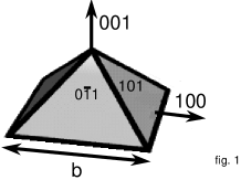
We assume the island is a simple square-based pyramid with -type planes for the sides, as shown in Fig. 1. The size of the island is parameterized by the length of the base, . The choice of island shape is somewhat arbitrary. There is no clear consensus on the exact shape, and it may vary with the details of growth conditions. The simple pyramidal geometry of Fig. 1 was chosen primarily because it has been used in previous calculations,[3, 4] hence facilitating comparisons.
An unavoidable consequence of Stranski-Krastanow island formation is that monolayers of island material remains on the substrate surface. This wetting layer is omitted from the calculations because it may be accounted for separately. The strain is insensitive to the wetting layer primarily because it is so thin, and also because it is biaxially strained to match the substrate lattice. The wetting layer does play a role in the electronic structure since it provides a quantum well state that is coupled to the quantum dot state. However, we are most interested in the tightly bound quantum dot states. For these states the wetting layer and quantum dot may be treated separately, simplifying the analysis of different wetting layer thicknesses.
After briefly outlining the calculational methods, we examine the strain-induced band structure, the single particle energies as a function of island size, and the exciton binding energy. Finally we compare the eight-band results with calculations using one, four, and six bands.
II Calculation
The technique used to obtain the electronic structure has been described previously, where is was used for a six-band calculation of InP islands embedded in GaInP. [5] Here we will focus on the differences due to the use of eight bands. The entire calculation is done on a cubic grid with periodic boundary conditions. First, the strain is calculated using linear continuum elastic theory. The strain energy for the system [8] is computed using a finite differencing approximation, and then minimized using the conjugate gradient algorithm.
The electronic structure is solved in the envelope approximation using an eight-band strain-dependent Hamiltonian, . [9] The kinetic piece of the Hamiltonian is
| (1) |
where
| (2) | |||||
| (3) | |||||
| (4) | |||||
| (5) | |||||
| (6) | |||||
| (7) | |||||
| (8) |
is the coupling between the conduction and valence bands, and are the (unstrained) conduction and valence-band energies respectively, and is the spin orbit splitting. The ’s are modified Luttinger parameters, defined in terms of the usual Luttinger parameters, , by
| (9) | |||||
| (10) | |||||
| (11) |
where is the energy gap, and .
The strain enters through a matrix-valued potential that couples the various components,
| (12) |
where
| (13) | |||||
| (14) | |||||
| (15) | |||||
| (16) | |||||
| (17) | |||||
| (18) |
is the strain tensor, and are the shear deformation potentials, is the hydrostatic valence-band deformation potential, and is the conduction-band deformation potential.
In addition to the explicit strain dependence in , there is a small piezoelectric effect which is included. The strain induced polarization of the material contributes an additional electrostatic potential which breaks the symmetry of the islands to . [3]
The energies and wave functions are computed by replacing derivatives with differences on the same cubic grid used for the strain calculation. The material parameters and strain in Eq.’s 1-5 vary from site to site. The Hamiltonian is then a sparse matrix which is easily diagonalized using the Lanczos algorithm. The calculation is further simplified by eliminating unnecessary barrier material, since bound states fall off exponentially within the barrier.
III Material Parameters
The values used for the various material parameters are given in Table I. All the parameters were set to the values corresponding to the local composition, except for the dielectric constant, , which was set to the value for InAs throughout the structure. Most parameters were taken from direct measurements, however a few merit comment. Neither nor have been directly measured, although the gap deformation potential has been measured. [10] Using the fact that for most III-IV semiconductors , [11] and can be estimated. Another important parameter is the unstrained valence-band offset, defined as in the absence of strain. The value used is based on transition-metal impurity spectra, and is in agreement with the value from Au Schottky barrier data. [12] The value is derived using the fact that transition metal impurities are empirically observed to have energy levels fixed with respect to the vacuum, relatively independent of their host environment. Thus, by comparing band edges referenced to the impurity levels in two different materials one deduces the relative band offsets if the strain could be turned off. The ground state energies of Mn impurities are and above the valence band in InAs and GaAs respectively [10], so the InAs valence band is above GaAs. TABLE I.: Material parameters. Unless otherwise noted, values are taken from Landolt-Börnstein. is the piezoelectric constant, is the relative dielectric constant, the ’s are the elastic constants, and is the lattice constant. Parameter InAs GaAs a a a b b c d -
IV Band Structure
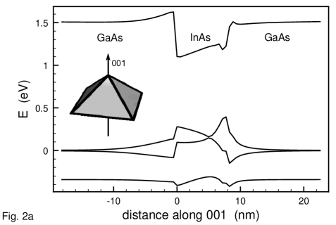
Some insight may be obtained by examining the strain induced modification to the band structure. Fig. 2 shows the band energies computed using the local value of the strain (i.e. the eigenvalues of Eq. 12 with ). Since the coupling between conduction and valence bands is proportional to , for the model reduces to a six-band model with a decoupled conduction band. The bands are shown for an island with . The band diagrams for a different sized island are obtained by simply rescaling the x-axes. The dominant effect of the strain is that the island experiences a large increase in its band-gap due to the considerable hydrostatic pressure. The conduction band still has a potential well deep at the base of the island, tapering to at the tip.
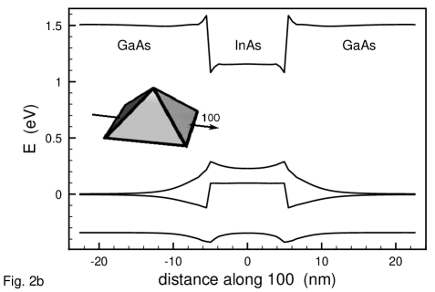
The valence band has a more complex structure. If we could somehow turn off the strain, the holes would be confined to the InAs by only . Strain alters this considerably, and makes the dominant contribution to the hole confinement. The most notable features are that the valence band is peaked near the tip of the island, with another high point near the base and a band crossing in between. This is most clearly seen in the plot of band energies along the direction. The plot along the direction near the base (Fig. 2b) shows that there is a slight peak in the valence band at the edge of the base, a feature shared with InP/GaInP islands. InP/GaInP islands also have such peaks in the valence band, and they are sufficiently strong that holes are localized near the peaks rather than spread out over the whole island.[5] In InP/GaInP islands there is also a valence band peak in the barrier material above the island which provides a separate pocket in which holes may be confined. From Fig. 2b we see that InAs islands have an elevation of the valence band above the island, but inside the island the valence-band edge is even higher. Hence we do not expect holes to be trapped in the barrier material.
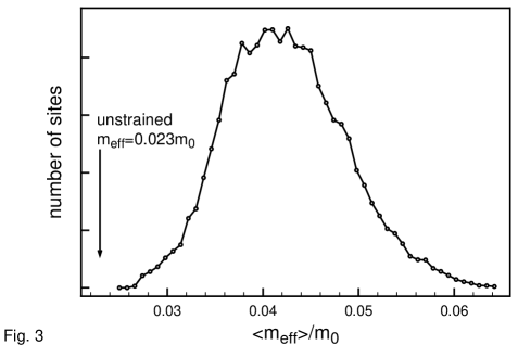
Strain-dependent effective masses may be found by computing the dispersion relation using the local value of the strain. Since is anisotropic, it is necessary to average over directions. The valence-band anisotropies are sufficiently strong that a hole effective mass is of dubious value. The conduction-band anisotropy is considerably smaller, however, making an electron isotropic effective mass a reasonable approximation. Fig. 3 shows a histogram of within the island. Due to the large hydrostatic strain, is doubled throughout much of the island, although there is considerable variation.
V Bound States
The bound state energies were computed as a function of island size using the full eight-band Hamiltonian (Fig. 4). Because the calculations were performed assuming no wetting layer there are states right up to the GaAs band edges. The energies for one and two-monolayer wetting layers are also shown in Fig. 4 for comparison. These were calculated as independent quantum wells using the envelope approximation. It should be noted that there will be a bound quantum dot state regardless of island size. It is a well known fact that in one and two dimensions an arbitrarily weak attractive potential has at least one bound state. In three dimensions there is no such guarantee, and hence it is possible to construct a quantum dot which has no bound states. However the wetting layer forms a quasi two-dimensional system with the island acting as an attractive potential. Therefore, we expect at least one wetting layer state to be bound to the dot, no matter how small it is.
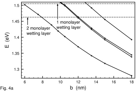
For the conduction-band there are only a few bound states in the island, as shown in Fig. 4a. The number of excited states in the quantum dot depends on the island’s size and the wetting layer thickness. In order to have an excited conduction-band state requires and for one and two monolayer wetting layers respectively. The first excited state is accompanied by a nearly degenerate state. The splitting between these two states varies from to for . The near degeneracy reflects the symmetry of the square island, with the splitting due to the piezoelectric effect. A third excited state appears for and for one and two monolayers respectively. These limits on are all upper bounds since the actual quantum dot energies will be lowered by the coupling to the wetting layer. In addition to the change in energy with size, the spacings vary as well. The gap between the ground state and first excited state varies from to over the range .
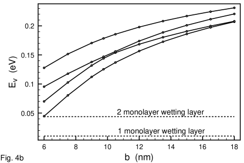
The valence-band states are more strongly confined, due to their larger effective mass. Only the first four states are shown in Fig. 4b, all of which lie well above the wetting layer energy. The energy spacings vary from a few meV to over the range of island sizes considered.
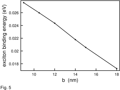
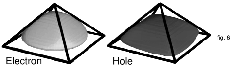
When the island is occupied by an electron and a hole, there will be additional binding energy from the coulomb interaction. Ground state exciton energies were computed in the Hartree approximation using eight-band solutions for both electrons and holes. That is, the exciton wave function was assumed to be of the form . and were found by self-consistent iteration, with convergence to within usually taking only two iterations. Fig. 5 shows the exciton binding energy as a function of island size. The results are in good agreement with single-band calculations [3], which is not surprising since the coulomb energy depends only on the charge density for the electron and hole parts of the wave function. The single-particle electronic Hamiltonian only affects the coulomb energy insofar as it alters the charge distribution. The exciton binding energy increases with decreasing island size, reaching for . Fig. 6 shows the exciton wave function for . In spite of the complex band structure seen in Fig. 2, the electron and hole wave functions appear ordinary. The wave functions are spread out over most of the island, with no signs of localization around smaller regions.
VI Comparison of Approximations
There remains the question of whether or not an eight-band model is worth the trouble. Previous authors have used various approximations to reduce the number of bands. Grundmann et. al. [3] treated the electrons and heavy holes as single particles moving in the strain induced potential corresponding to the band edges. The effective masses were different in the island and barrier materials, but took constant unstrained values within each region. As was pointed out by Cusack et. al. [4] the narrow InAs band gap leads to significant band mixing, resulting in large strain induced shifts in the effective mass. Based on a pseudopotential calculation, Cusack et. al. set for the conduction band, which is the value predicted for bulk InAs under the average hydrostatic strain in the island. The valence-band states were calculated using a four-band model. Note that is in good agreement with the peak of the distribution for shown in Fig. 3.
Unfortunately, a comparison with previous calculations is complicated by the fact that the methods have differed in more than the Hamiltonian. Different material parameters were used, the strain was calculated differently (continuum elasticity [3] versus valence force field method [4]), and different numerical techniques were used to solve Schrödinger’s equation (real space differencing [3] versus a plane wave basis [4]). To more directly compare these different approximations, energies were calculated using several different Hamiltonians, but all using the same grid and strain profile. For the conduction band the methods considered are (i) setting set to its unstrained values of in the InAs, and in the GaAs, (ii) using the value corresponding to the average hydrostatic strain in the InAs , and using in the GaAs, (iii) using a spatially-varying strain-dependent , (iv) using full eight-band Hamiltonian.
A comparison of the different conduction-band energies for is shown in Fig. 7a. The dominant feature is that the energies decreases as the Hamiltonian includes more physics. For the simple unstrained effective mass only a single state is found. With the binding energy of the ground state increases by . Also, the nearly degenerate first and second excited states are brought below the energy of a one-monolayer wetting layer. Using a one-band model with gives energies very close to those for . The eight-band results are significantly different. Not only is the ground state lower by another , but the two nearly degenerate excited states are clearly confined. In addition, a third excited state falls below the the one-monolayer energy. The one-band models with and both predict . The eight-band model predicts .


The valence-band energies were calculated using four, six and eight-band models (Fig. 7b). The differences are less dramatic than for the conduction-band states. The four and eight-band ground state energies agree to within . For six bands, however, the ground state energy differs from the other two by . At first sight this is surprising, since one generally expects the more complicated model to produce more accurate results. However, for InAs so if either the conduction or split-off band is to be included, then both should be. The six-band model violates this requirement by allowing mixing of the valence-band states, but leaving the conduction band decoupled. The eight and four-band models do predict slightly different level spacings, but the basic pattern is the same. is large ( for four bands, for eight bands) with a smaller spacing between excited states ( and for four and eight bands respectively).
An interesting way of viewing the model dependence of the energy is to compare with the size dependence. As a simple example, comparison of Fig.’s 4a and 7a shows that a island calculated with gives the same ground state energy as the eight-band model at . Hence, if the uncertainty in the island geometry is greater than we would expect these inaccuracies to dominate the errors in the electronic structure results. This gives an indication of the importance of specifying the correct island geometry.
VII Conclusions
Coupling the valence and conduction bands has a strong impact on the spectrum of InAs quantum dot states. The eight-band model gives results significantly different than one, four, and six-band approximations. It predicts larger binding energies and strongly confined excited states which do not appear in one-band approximations.
The results presented here clearly demonstrate the need for eight-band calculations, or perhaps even more complex techniques such as pseudopotentials.[6] While large scale calculations using complex Hamiltonians have become feasible, the results are no better than the input parameters used. Accurate agreement between theory and experiment will require precise measurements of the island geometry.
I wish to thank Mats-Erik Pistol, Mark Miller, and Jonas Ohlsson for enlightening comments and discussions.
REFERENCES
- [1] e-mail: cpryor@zariski.ftf.lth.se
- [2] J. -Y. Marzin and G. Bastard, Solid State Commun. 91, 39 (1994).
- [3] M. Grundmann, O. Stier, and D. Bimberg, Phys. Rev. B 52, 11969 (1995).
- [4] M. A. Cusack, P. R. Briddon, and M. Jaros, Phys. Rev. B 54, 39 (1996).
- [5] C. Pryor, M-E. Pistol, L. Samuelson, http://xxx.lanl.gov/abs/cond-mat/9705291
- [6] H. Fu, A. Zunger, Phys. Rev. B 55, 1642 (1997).
- [7] O. Stier, D. Bimberg, Phys. Rev. B 55, 7726 (1997).
- [8] L.D. Landau and E.M. Lifshitz, Theory of elasticity, (Pergamon, London, 1959).
- [9] T. B. Bahder, Phys. Rev. B 45, 1629 (1992); T. B. Bahder, Phys. Rev. B 41, 11992 (1990);
- [10] Semiconductors, edited by O. Madelung, M. Schilz, and H. Weiss, Landolt-Börnstein, Numerical Data and Functional Relations in Science and Technology Vol. 17 (Springer-Verlag, New York, 1982).
- [11] D. D. Nolte, W. Walukiewicz, and E. E. Haller, Phys. Rev. Lett. 59, 501 (1987);
- [12] S. Tiwari and D. J. Frank, Appl. Phys. Lett. 60, 630 (1992).
- [13] S. Adachi, J. Appl. Phys. 53, 8775 (1982).