[
to appear in Phys. Rev. B
Edge effects in a frustrated Josephson junction array with modulated
couplings
Abstract
A square array of Josephson junctions with modulated strength in a magnetic field with half a flux quantum per plaquette is studied by analytic arguments and dynamical simulations. The modulation is such that alternate columns of junctions are of different strength to the rest. Previous work has shown that this system undergoes an followed by an Ising-like vortex lattice disordering transition at a lower temperature. We argue that resistance measurements are a possible probe of the vortex lattice disordering transition as the linear resistance with at intermediate temperatures due to dissipation at the array edges for a particular geometry and vanishes for other geometries. Extensive dynamical simulations are performed which support the qualitative physical arguments.
pacs:
74.50+r, 74.60.Ge, 64.60.Cn]
There has been a lot of interest in arrays of superconducting grains coupled by Josephson junctions. In the absence of a magnetic field perpendicular to the plane of the array, such a system is rather well described by a classical two dimensional model and experimental transport measurements [1] are well described by the dynamical extension[2] of the static theory[3, 4]. The most recent technique employed to measure truly equilibrium properties of a superconducting array is a magnetic flux noise measurement[5] which does not require an imposed current. Earlier experimental studies measured the voltage due to an applied zero frequency current [6, 7, 8, 9, 10, 11, 12] and the frequency dependent impedance by two coil mutual inductance techniques [1]. The agreement between theory and experiment is quite good. In the presence of a magnetic field normal to the array, the situation is not so clear as, even in the simplest case of half a flux quantum per elementary plaquette on a square lattice, the system is much more complicated and less well understood. Even in the absence of disorder, which is inevitably present in an experimental system[12], there are two types of competing order when : a discrete symmetry of the ground state of the vortex lattice and the symmetry of the superconducting order parameter. In an isotropic system where all the junction strengths are the same the phase coherence of the superconducting order parameter must be destroyed at a lower temperature or, at best, the same temperature as the discrete order of the vortex lattice [13]. The most recent simulations on this[14, 15] agree that the phase order is destroyed by a transition at a very slightly lower temperature than the discrete order which undergoes a transition in the Ising universality class.
An interesting variant of the isotropic square array with was proposed by Berge et al[16] in which alternate columns of junctions are of different strength to the rest. This model is described by the Hamiltonian
| (1) |
where on all nearest neighbor bonds except on alternating columns where . where is the vector potential of the external magnetic field and is the quantum of flux. The frustration of plaquette is where the sum is over the bonds surrounding the plaquette. It is a gauge invariant definition and a convenient gauge is the Landau gauge in which on every second column of bonds and otherwise. Such an array is experimentally realizable by varying the area of the appropriate junctions to obtain alternating columns of strength and is currently being investigated [17]. The model described by Eq.(1) has been studied numerically[16, 18, 19] and it was found that, by varying the anisotropy parameter , the order of the and Ising transition is reversed. In the isotropic system at the transition occurs at a lower temperature than the Ising transition but when is sufficiently large the Ising is at a lower temperature than the transition. The early simulations were unable to separate the transitions for but later work[14, 15] provided convincing evidence for two separate transitions with . Another generalized version of the square array at has been considered recently [20] in which the couplings in Eq. (1) are modulated in the and directions simultaneously, in a zig-zag pattern. In this case, varying in the range does not lead to a change in the order of the and transitions and they critical properties remain the same as for the isotropic square array.
In a two dimensional plane of superconductor in a magnetic field normal to the plane a vortex lattice is formed. If a vortex is subjected to a force due to an external applied current, it will move in a direction perpendicular to the current and this creates a voltage where is the density of free vortices, which implies a finite linear resistance. This is regarded as signalling the destruction of superconductivity. An array of Josephson junctions with no disorder in a magnetic field with a frustration has a ground state which is a vortex lattice commensurate with the underlying lattice and is pinned and superconducting. As the temperature is raised, the vortex lattice will melt or become a floating phase which is not pinned. In either case, one would naively expect that the system becomes non superconducting as the vortices will move and induce a voltage when an external current is applied. In particular, a square array with and has a ground state [16] which is a vortex lattice with a vortex in every second plaquette commensurate with the underlying lattice. Since the vortex lattice is pinned by commensurability effects, the system will be superconducting and should become non-superconducting when the lattice melts. In the anisotropic array of Eq.(1), the vortex lattice melts by an Ising transition at but order (superconductivity) persists to higher temperatures [16, 18] although the vortex lattice has melted, which seems to contradict the standard folklore that, when the vortex lattice melts, superconductivity disappears. It seems to us that there are three possibilities to reconcile the equilibrium behavior of the anisotropic system of Eq.(1) with these qualitative arguments about the transport properties with a small applied current at intermediate temperature where the vortex lattice is melted: (1) the present understanding of the effect of the melting of a vortex lattice on superconductivity is wrong; (2) the equilibrium calculations at have no relation to the dynamics as ; (3) the properties of the melted vortex lattice in the anisotropic array are special and the qualitative argument that superconductivity is destroyed by the melting does not apply.
In this paper, we take the view that the system of Eq.(1) is special and that scenario (3) is the explanation and also address the question of the signature (if any) of the low temperature Ising transition in experimental measurements[17] on an anisotropic array with column modulation. Two coil mutual inductance experiments measure the dynamical impedance which is proportional to the inverse of the helicity modulus [1] . At the Ising transition, this has a harmless singularity of the form[18, 19] where which implies that the impedance will also not show any divergence as observable signature. The implications for the flux noise spectrum have not been worked out and it would be of some interest to do this. There is one possibility which is the linear resistance which we discuss in the rest of this paper. We study by qualitative analytical methods and by numerical simulations the zero frequency characteristics of an anisotropic array and show that the onset of linear resistance occurs at the low temperature Ising transition, which may be detectable by experiment. This is an edge effect and, in an array, the linear resistance with when . We begin by defining the model and argue that the onset of linear resistance is due to the formation and growth of domains of reversed chiral order at the edges of the array. The geometry of the array and the direction of the applied current is important, and we first define the various geometries and boundary conditions and what is to be expected on physical grounds in each case. We then discuss the results of numerical simulations and show that these are consistent with our analytical arguments.
The low temperature Ising transition may be described in terms of the proliferation of domain walls separating regions of different ground states. A ground state configuration of Eq.(1) may be represented in the Coulomb gas representation by a set of unit charges in a checkerboard pattern on half the sites of the dual lattice[18]. The important low energy excitations which destroy the Ising order are domain walls between regions of different Ising order and these domain walls lie along the bonds of the original lattice. It is well known that there are fractional charges at the corners of these domain walls[22, 23, 24]. One may argue that such domains with a net integer charge formed of corner charges of the same sign are the excitations which undergo a unbinding transition at the same temperature as the Ising transition. However, numerical simulations[14, 15, 16, 18] show that the and Ising transitions are separated for almost all values of the anisotropy parameter which implies that the fractional corner charges and the integer charges do not screen each other. In the case of interest here, sufficiently large, one can understand this by considering the domain walls at . As shown by Eikmans et al.[18], the domain walls between regions of different Ising ground states lie along the strong bonds since the energy of these is less than those on the weak bonds. In fact, they find numerically that there is a negligible density of domain walls on weak bonds for but the density on the strong bonds grows rapidly when . Thus, these domains carry zero net charge as the fractional corner charges must alternate between . For a domain to have an integer charge, one of the vertical walls must lie along a weak bond which costs a lot of free energy. The unit cell describing the Ising degree of freedom may be taken to be four adjacent elementary plaquettes bounded by strong bonds as shown in Fig. (1) and at domains with an integer number of these unit cells will proliferate. Since these domains carry zero net charge and zero dipole moment, they cannot contribute to the linear resistance which is proportional to , the concentration of thermally excited free charges (vortices)[2]. Because of the zero dipole moment, the mechanism of stretching of domains by the applied current suggested by Mon and Teitel [21] as a contribution to the non linear resistance for of the form , where is the domain wall free energy, is not a dominant effect for the anisotropic arrays considered in this paper.
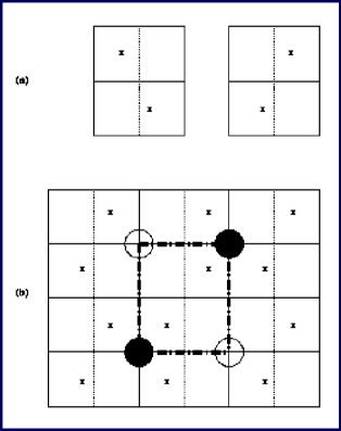
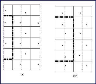
We consider a lattice of elementary plaquettes corresponding to a lattice of superconducting grains coupled by weak links. There are two geometries to consider (a) columns of weak bonds at the two vertical edges and (b) columns of strong bonds at the edges as sketched in Figs.(2a) and (2b). In case (b), there are complete unit cells and the current is injected uniformly in the direction perpendicular to the weak bonds. A linear resistance is due to the current driving the pre-existing thermally excited charges across the system but such charges do not exist in the bulk because, near the Ising transition, only neutral domains are present as the domain walls are constrained to lie along the strong bonds[18]. One may expect that free, unbound fractional charges exist near the edges of the array because of domain formation at the edges. We expect that for the system will consist of a set of domains of opposite Ising order of size determined by the bulk correlation length in the bulk and at the edges for free boundary conditions by the surface correlation length with [25]. The amplitudes and are nonuniversal but their ratio is universal and is given in terms of critical exponents from conformal invariance[27] by
| (2) |
with the bulk and edge exponents [25, 26, 27] and which implies that the density of edge domains is larger than that in the bulk of the array. This is of no significance for the linear resistance in arrays where the strong bonds are at the edges as in Fig. (2b) as there are no net fractional charges at the ends of these edge domains and these will behave just like the domains in the bulk of Fig. (1b) which carry no net charge. The situation for arrays with weak bonds at the vertical edges is very different and this is shown in Fig. (2a). In this geometry, one can regard these edges as splitting the unit cells of Fig. (2a) in half thus forcing fractional charges of opposite signs at the two ends of the domains. Since , the domain walls may be regarded as having melted and having zero line tension as the edge undergoes an ordinary transition slaved to the bulk transition[26]. Along the edges of the array of linear size , these charges are effectively free unbound charges of concentration . This implies that in an array with weak bonds at the vertical edges as in Fig. (2a) there will be a linear resistance
| (3) |
provided there are free boundary conditions at these edges. This can be realized by uniform current injection. Other methods of current injection such as injection from superconducting busbars will suppress this effect as the busbars repel the vortices (charges) from the edges and the linear resistance will be reduced to [28, 29] as in arrays with strong bonds at the vertical edges.
To check the above qualitative predictions, we have performed simulations on arrays of both geometries and with both uniform current injection and injection from superconducting busbars. Also, to avoid the effects of finite applied current which causes a non linear relation in the thermodynamic limit[2, 28], we have computed the linear resistance from a linear response expression in terms of equilibrium quantities. Our simulations are performed using the Langevin dynamical method of Falo et al.[30] . We assume that the junctions on alternate columns have critical currents and elsewhere and are shunted by equal resistances . Each superconducting grain has a small capacitance to ground. The dynamical equations for the phases and the voltages of the grain at site follow from charge conservation and the Josephson equation
| (4) | |||||
| (5) | |||||
| (6) |
where on all horizontal bonds and on alternating vertical bonds as in Fig .(1) and the sums over are over the nearest neighbors of site . The thermal noise current on the bond is Gaussian distributed and obeys the fluctuation dissipation theorem
| (7) |
For the columns of grains at either edge of the array labelled by
| (8) | |||||
| (9) | |||||
| (10) | |||||
| (11) |
where is the current per bond injected into each grain on the left column and extracted from each grain on the right column. For convenience, we choose system sizes with the number of columns an odd integer with free boundary conditions at the left and right hand edges and the number of horizontal rows an even integer with periodic boundary conditions in the vertical direction. We choose to use the Landau gauge where on all horizontal bonds, on the odd numbered vertical columns (first, third, , last) and on even numbered columns. This is a particularly convenient choice of lattice size and gauge as it permits an integer number of unit cells and also for a simple formulation when superconducting busbars are connected to the left and right hand edges of the array by a set of junctions as the phase and voltage on each busbar is then -independent. The equations governing these phases , and the voltages , are then[29]
| (12) | |||||
| (13) | |||||
| (14) | |||||
| (15) | |||||
| (16) |
Here the sums over are over the sites connected to the busbars. The mean voltage drop across the system is given by
| (17) |
where is the phase difference across the array at time and is the run time of a simulation. The temperature is measured in units of and the time is in units of , the inverse Josephson plasma frequency. A time step of typically in these units [29] was used in the numerical integration. Changing the time step does not change the results. Most of our simulations have been done on small systems with and with periodic boundary conditions in the direction. In any event, we found that boundary effects in the transverse direction are not significant to the accuracy of our simulations.
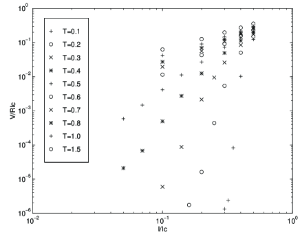
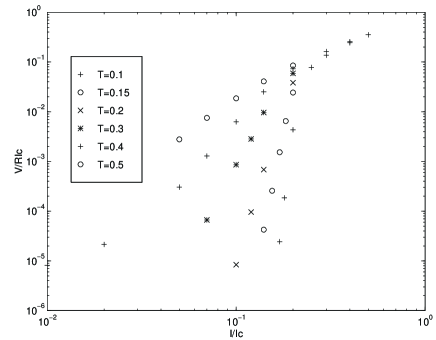
The relation is shown in Figs.(3) and (4) for the anisotropy parameter at different temperatures with the current applied perpendicular to the weak bonds using the method of uniform injection described by Eq.(11) with periodic boundary conditions in the transverse direction. For the array of Fig. (2a), the onset of linear Ohmic behavior is consistent with the data for which is close to the estimate of the Ising critical temperature for this value of . When the geometry is changed so that the strong bonds are at the edges as in Fig. (2b), Ohmic behavior is observed only at higher temperatures , which is closer to the estimate of the transition at as expected. For , as expected from the qualitative arguments, the situation is reversed and the results of the simulations are shown in Fig. (5) for arrays with the or strong bonds at the edges as in Fig. (2a) and in Fig. (6) for arrays of with the bonds not at the edges as in Fig. (2b). In the latter case, the onset of linear dissipation is observed at , close to while in the former case at , closer to the transition. Again this agrees with our qualitative arguments.


When the applied current is finite, the relation always has a non-linear contribution. The resistance, defined by , is proportional to for in the thermodynamic limit which may obscure the small predicted linear resistance of . To obtain a more definitive signature which is free of these non-linear finite current effects, one can define the linear resistance by a Kubo formula in terms of an equilibrium voltage-voltage correlation function at
| (18) |
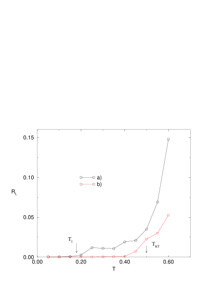
where is the total size-dependent voltage across the array. The results of the dynamical simulation using the Kubo expression of Eq.(18) at are shown in Fig. (7) together with those from a simulation with , the lowest accessible current, and defining . This is always larger than the value obtained from Eq.(18) because of the non-linear contribution when . This can be regarded as confirmation of our arguments that the onset of linear dissipation at is not an artifact but a real effect caused by the Ising transition and may be observable by experiment. Our results for arrays of size with and periodic boundary conditions in the direction are summarized in Fig. (8) where we show the linear resistance computed from the Kubo expression of Eq.(18) for arrays geometries of Fig. (2a) and Fig. (2b). From this it is clear that there is an onset of linear resistance around when the weak bonds are at the edges and at a higher temperature when strong bonds are at the edges. Our results for the phase diagram in the plane are shown in Fig. (9) where we plot determined by purely equilibrium Monte Carlo simulations and also by the onset of for arrays of Fig. (2a) from Eq.(18). To the accuracy of our simulations, the two methods agree providing additional evidence to support our qualitative arguments. As a final check, we performed a series of simulations at finite on larger systems up to to check the prediction of Eq.(3 ) for and in Fig. (10) we show for several values of and we see that this is consistent with being an -independent constant although the errors are fairly large.


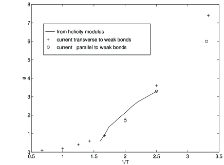
The temperatures at which the onset of linear resistance occurs is consistent with the Ising critical temperature and happens for arrays of Fig. (2a) when and Fig. (2b) when . This suggests that the linear resistance observed when is a result of both Ising disorder and free boundary conditions at the array edges allowing for motion of fractional charges induced by the domains, as predicted by qualitative arguments. The presence of weak bonds at the edges of the arrays of Fig. (2a) for and of Fig. (2b) for is not essential as changing the strength of the edge bonds does not change the scenario in any qualitative way but only quantitatively. The determining factor is that the periodicity of the Ising domain walls is two lattice spacings which is a consequence of the energy of a domain wall on a weak bond being larger than on a strong bond for and the reverse for . When the edges correspond to a weak bond, domains at edges have width unit cells which implies that there are free fractional charges at the ends of these domains in thermal equilibrium and these are free to move under the influence of an applied current. The strength of the edge bonds does not affect the argument in any essential way except to alter the magnitude of the dissipation. We have checked that the dissipation onset at is in fact an edge effect by performing simulations in a busbar geometry where the current is injected and extracted by attaching the edges of the array to superconducting busbars[29] described by Eq.(16). In this geometry, fractional charges (vortices) are repelled from the edges and domain formation is suppressed, thus minimizing or completely suppressing edge contributions to the dissipation. The relation for such an array of Fig. (2a) with is shown in Fig. (11) for the current normal to the weak bonds and in Fig. (12) for parallel to the weak bonds. There is good agreement between the relations of Fig. (11) and Figs.(4,5) in which there are strong bonds at the edges and where we expect there to be no linear contribution. One also observes that the slopes of the curves in the busbar geometry are independent of the direction of as the slopes in Figs.(11) and (12) are the same for the same temperature . This slope is plotted in Fig. (13) together with that deduced from the helicity modulus [18] by [28] . The agreement between the different methods is by no means perfect but we believe the numerical support for our qualitative predictions is more than adequate to demonstrate their validity.

The conclusion we reach is that the low Ising transition in anisotropic arrays of Josephson junctions does have an effect which may be observable in zero frequency transport measurements. This effect is the onset of a linear resistance at in arrays of the appropriate geometry. Although this is an edge effect with it should be large enough to be measurable in an array of reasonable size. This onset is an unambiguous signature of the low Ising transition as, in the thermodynamic limit and bulk finite size corrections to this will decay very rapidly with increasing and should be negligible compared to the contribution discussed here. These bulk finite size effects can be estimated by performing the same measurement with the current parallel to the weak bonds when the contribution to will be absent, which provides a method of assessing the feasibility of the proposed measurement. This small edge contribution to the linear resistance is a real effect which is a signal of the bulk Ising transition but, as is well known, the interpretation of such measurements is very difficult at temperatures well below the temperature because of screening effects[1, 31]. We have not attempted to take such effects into account in this work but there is a possibility that they may invalidate our conclusions. Clearly this should be investigated as should various other effects such as disorder in the junction strengths which will inevitably be present in a real system, vortex and domain wall pinning etc. It is not very aesthetically satisfying that one must resort to an edge effect detectable by a voltage measurement at finite current as there are limits to the sensitivity of this, especially because a typical experimental array[17] is much larger than those of this work so that the dissipation at the edges will be much smaller than in our simulations. In fact, in the thermodynamic limit the linear dissipation in the temperature range where the vortex lattice is melted should vanish. It would be much more satisfying if some equilibrium bulk quantity would give a signal of the Ising transition but in view of the very weak signal in the helicity modulus [18, 19], this will be a very difficult effect to observe. There is the possibility that a flux noise measurement similar to that of Shaw et al.[5] may show a detectable signal of the Ising transition. However, naively this seems not very hopeful as the noise spectrum basically measures the time dependent correlation function where is the total vorticity (charge) enclosed by the squid detector. Since the Ising transition is signalled by the proliferation of domains with fractional corner charges but with zero net charge, as in Fig. (1b), it is difficult to see how these can contribute significantly to the correlation function determining the noise spectrum. However, this is still worth investigating as it is one of the few remaining possibilities to detect this elusive transition.
Acknowledgements.
This work was supported by the IAE agency/ICTP (E.G.) and by a joint NSF-CNPq grant (E.G.and J.M.K.). The authors thank H. Pastoriza and P. Martinoli for correspondence about their experimental results prior to publication. Some of the computations were performed at the Theoretical Physics Computing Facility at Brown University.REFERENCES
- [1] P. Martinoli, Ph. Lerch, Ch. Leemann and H. Beck, Jap. Journ. Appl. Phys., 26, 1999, (1987)
- [2] V. Ambegaokar, B.I. Halperin, D.R. Nelson and E.D. Siggia, Phys. Rev. B21, 1806, (1980)
- [3] J.M. Kosterlitz and D.J. Thouless, J. Phys, C6, 1181, (1973)
- [4] J.M. Kosterlitz, J. Phys. C7, 1046, (1974)
- [5] T.J. Shaw, M.J. Ferrari, L.L. Sohn, D.-H. Lee, M. Tinkham and J. Clarke, Phys. Rev. Lett. 76, 2551, (1996)
- [6] D.J. Resnick, J.C. Garland, J.T. Boyd, S. Shoemaker and R.S. Newrock, Phys. Rev. Lett. 47, 1542, (1981)
- [7] D.W. Abraham, C.J. Lobb, M. Tinkham and T.M. Klapwijk, Phys. Rev. B26, 5268, (1982)
- [8] R.F. Voss and R.A. Webb, Phys. Rev. B25, 3446, (1982)
- [9] R.A. Webb, R.F. Voss, G. Grinstein and P.M. Horn, Phys. Rev. Lett. 51, 690, (1983)
- [10] M. Tinkham, D.W. Abraham and C.J. Lobb, Phys. Rev. B28, 6578, (1983)
- [11] R.K. Brown and J.C. Garland, Phys. Rev. B33, 7827, (1986)
-
[12]
B.J. van Wees, H.S.J. van der Zant and J.E. Mooij, Phys.
Rev. B35, 7291, (1987)
H.S.J. van der Zant, H.I. Rijken and J.E. Mooij, J. Low Temp. Phys. 79, 289, (1990); 82, 67, (1991) - [13] E. Granato, J.M. Kosterlitz, and M.P. Nightingale, Physica B 222, 266 (1996) and references therein.
- [14] P. Olsson, Phys. Rev. Lett. 75, 2758, (1995)
- [15] S. Lee, K.-C. Lee and J.M. Kosterlitz, preprint cond-mat 9612242; to be published Phys. Rev. B
- [16] B. Berge, H.T. Diep, A. Ghazali and P. Lallemand, Phys. Rev. B34, 3177, (1986)
- [17] H. Pastoriza and P. Martinoli, private communication
- [18] H. Eikmans, J.E. van Himbergen, H.J.F. Knops and J.M. Thijssen, Phys. Rev. B39, 11759, (1989)
- [19] E. Granato and J.M. Kosterlitz, J. Appl. Phys. 64, 5636, (1988)
- [20] M. Benakli and E. Granato, Phys. Rev. B 55, 8361 (1997).
- [21] K.K. Mon and S. Teitel, Phys. Rev. Lett. 62, 673 (1989)
- [22] T.C. Halsey, J. Phys. C18, 2437, (1985)
- [23] S.E Korshunov, J. Stat. Phys. 43, 17, (1986)
- [24] J.M. Thijssen and H.J.F. Knops, Phys. Rev. B37, 7738, (1988)
-
[25]
B.M McCoy and T.T. Wu, Phys. Rev. 162, 436, (1967)
B.M. McCoy and J.H.H. Perk, Phys. Rev. Lett., 44, 840, (1980) - [26] K. Binder, Phase Transitions and Critical Phenomena, C. Domb and J.L. Lebowitz, eds., Vol.8, p.1, (1983)
- [27] J.L. Cardy, J. Phys. A17, L384, (1984); Phase Transitions and Critical Phenomena, C. Domb and J.L. Lebowitz, eds., (Academic Press, London), Vol.11, p.55, (1987)
- [28] B.I. Halperin and D.R. Nelson, J. Low Temp. Phys. 36, 599, (1979)
- [29] M.V. Simkin and J.M. Kosterlitz, Phys. Rev. B55, 11646, (1997)
- [30] F. Falo, A.R. Bishop and P.S. Lomdahl, Phys. Rev. B41, 10893, (1990)
- [31] P. Martinoli, Ch. Leeman and Ph. Lerch, Non-linearity in Condensed Matter, eds. A.R. Bishop, D.K. Campbell, P. Kumar and S.E. Trullinger, (Springer Series in Solid State Sciences, Berlin) Vol.69, p.361, (1987)