Comparison of Zn1-xMnxTe/ZnTe multiple-quantum wells and quantum dots by below-bandgap photomodulated reflectivity
Semicond. Sci. Technol. 11, 1863-1872 (1996)
cond-mat/9710008)
Abstract
Large-area high density patterns of quantum dots with a diameter of 200 nm have been prepared from a series of four Zn0.93Mn0.07Te/ZnTe multiple quantum well structures of different well width (40 Å, 60 Å, 80 Å and 100 Å) by electron beam lithography followed by Ar+-ion beam etching. Below-bandgap photomodulated reflectivity spectra of the quantum dot samples and the parent heterostructures were then recorded at 10 K and the spectra were fitted to extract the linewidths and the energy positions of the excitonic transitions in each sample. The fitted results are compared to calculations of the transition energies in which the different strain states in the samples are taken into account. We show that the main effect of the nanofabrication process is a change in the strain state of the quantum dot samples compared to the parent heterostructures. The quantum dot pillars turn out to be freestanding, whereas the heterostructures are in a good approximation strained to the ZnTe lattice constant. The lateral size of the dots is such that extra confinement effects are not expected or observed.
1 Introduction
A subgroup of the dilute magnetic semiconductors (DMS) is formed by alloys consisting of a II-VI host material with Mn2+ ions substituted for some of the
group II cations (e.g. Zn1-xMnxTe, Cd1-xMnxTe and Zn1-xMnxSe). The most prominent feature of these Mn-containing DMS materials is the s,p-d exchange interaction between the d-electrons of the Mn2+ ions and the free charge carriers in the conduction and valence bands, which leads to magnetic splittings at low temperatures of the order of 100 meV (for a review of these properties see [1, 2]). In recent years, heterostructures such as multiple quantum wells (MQWs) containing DMS materials have been grown very sucessfully by several groups. Progress has been made in the understanding of the properties of Mn at the heterointerfaces [3, 4]. It is now possible to use this knowledge to make detailed studies, by magnetic field experiments, of aspects of epitaxial growth such as asymmetric interfaces [5] and donor distributions in MQW samples [6],
demonstrating that DMS systems are ideal model systems for the study of semiconductor heterostructures. These II-VI DMS alloys are also of interest since they are closely related to the II-VI wide-bandgap alloys such as Zn1-xCdxSe used in blue-green optoelectronic devices.
The free carriers and the excitons in heterostructures are confined in one dimension forming a two-dimensional (2D) quantum system. It is of interest from the viewpoint of fundamental physics, as well as that of applications in device manufacturing, to reduce the dimensionality of quantum systems further, to one-dimensional (1D) systems such as quantum wires or even zero-dimensional (0D) systems such as quantum dots (Q-dots). There are several approaches by which one can achieve this, including the direct growth of 1D or 2D systems or the controlled etching of heterostructures. Some examples of direct growth techniques of III-V and II-VI 1D and 0D structures are the growth of microcrystallites [7, 8], growth on patterned substrates [9, 10], cleaved edge overgrowth [11, 12], strain modulation by using sputtered stressors [13, 14] and self-organized growth [15, 16]. The controlled etching techniques are all based on a lithography process to create an etch pattern followed by an etching process. Several techniques for etching II-VI materials have been used: ion beam etching (IBE) [17], wet etching [18, 19], reactive ion etching (RIE) [20, 21] or combinations of the three techniques. Similar techniques have been used for III-V materials (for an overview. see [22]). The smallest Q-dot sizes achieved by etching of II-VI materials are of the order of 30 nm in diameter, which is close to the size at which additional confinement effects are significant [23]. Nevertheless, the study of Q-dots of bigger diameter can yield valuable information about changes in the strain state of the specimen or about the damage caused by the nanofabrication process. Two main techniques are used to study the strain contributions in nanostructures. These are X-ray diffractometry [24-26] and photomodulated reflectivity [27-30] and both reveal that, in most cases, a relaxation towards a freestanding structure takes place in quantum dots and quantum wires. The damage induced by the nanofabrication process has been investigated by time-resolved and continuous wave photoluminescence spectroscopy [31-33] and Raman spectroscopy of phonons [34]. So far, only a few 1D or 0D DMS structures have been prepared, all in the Cd1-xMnxTe/CdTe system [28, 35-37] .
We report here on a study of the strain states in a series of four 200 nm diameter Zn1-xMnxTe/ZnTe MQWs quantum dot samples (and their parent heterostructures) using below-bandgap photomodulated reflectivity (BPR). In the BPR technique, the reflectivity of the sample is modulated by laser light whose energy is below the band gap of the semiconductor material; BPR was first reported as a new technique by Bhimnathwala and Borrego [38], although it was already applied before by Rockwell et al. [39]. We have established that BPR spectra contain the same spectroscopic information as conventional photomodulated reflectivity spectra [40]. We have tried to gain some insight into the modulation mechanism of BPR and have shown that it is likely to result from the excitation of deep levels in the semiconductor material [41].
2 Experimental details
The four MQW samples were grown by molecular beam epitaxy (MBE) on (001)-oriented GaSb substrates. Each heterostructure consists of a 1000 Å buffer layer followed by 10 ZnTe quantum wells embedded between Zn0.93Mn0.07Te barriers. The four samples are of different quantum well width 40 Å, 60 Å, 80 Å and 100 Å respectively and the barrier thickness is 150 Å in all cases. Further details of the MBE growth can be found in [40].
The nanofabrication of the quantum dots was carried out in eight steps. First, the specimen was cleaned with acetone in an ultrasonic bath and rinsed with isopropanol. In the second step, it was spin-coated with a two-layer resist consisting of a 140 nm
bottom layer of copolymer P(MMA-MAA) and a 50 nm top layer of 950k PMMA. Afterwards, the electron beam lithography was carried out with a JEOL JBX 5DII system with CeB6 cathode using an acceleration voltage of 50 kV, a final aperture of 60 m,
a working distance of 14 mm and a beam current of 1 nA. The patterned area covered mm2 on the specimen. We exposed nm2 squares with a nominally homogeneous dose of 220 C/cm2. These squares were arranged on a square lattice with a lattice constant of 400 nm. The diameter of the beam and the proximity effect result in a circular exposure profile under these conditions. In the fourth step, the exposed sample was developed in a solution of 20 mL isopropanol and 2 mL distilled water for 60 s. Afterwards, a 30 nm Ti film was deposited on the resist mask, and after subsequent lift-off in warm acetone, a pattern of circular Ti dots with a diameter of about 200 nm to 220 nm was obtained. This pattern was transferred onto the semiconductor using Ar+ IBE under normal incidence with a relatively low accelaration voltage of 200 V and a current density of 0.16 mA/cm2. With these parameters, about 20 min were requried to etch through the heterostructure to a depth of about 30 nm. In the final, eighth step the Ti etch mask was removed with hydrofluoric acid. After each process step, the samples were inspected by scanning electron microscopy (SEM).
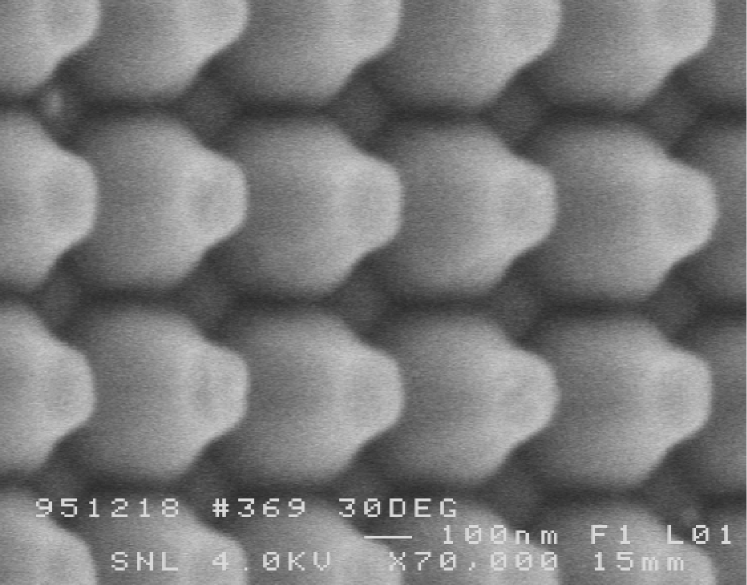
Figure 1 shows an SEM image of the high density pattern of 200 nm Q-dots prepared on the Zn0.93Mn0.07Te/ZnTe heterostructure with 80 nm quantum well width. The ten quantum wells are situated in the top two-thirds of the dots. The image was taken with the specimen tilted by 30∘ and the Ti mask has been removed. The inspection with the SEM showed that the size of the dots as well as the period of the dot lattice are both homogeneous throughout the whole mm2 area. We have obtained a high density of dots, close to the attempted ratio of the area covered by dots to the etched area of . There are only a few regions with defects in the dot pattern (not shown in figure 1). These originate mainly from macroscopic defects such as scratches and dust particles already on the sample before the nanofabrication process and were not caused by the process itself. The shape of the individual dots shows an inclination of the side walls, which is typical for IBE etched samples [42]. There are two main reasons for this inclination in IBE: erosion of the metal mask and redeposition of etched materials. A stronger erosion of the edges of the Ti mask compared to the central mask region occurs due to the angle dependence of the Ti etching rate. This sucessive reduction of the metal mask is then transferred into the semiconductor as the etching continues resulting in different etching depths. Because of the low acceleration voltage of the Ar+ ions, the sputtered atoms are of low energy and are simply redeposited on opposite surfaces. The inclination observed in our samples is about 25∘ which is larger than the 10∘ to 15∘ observed by other groups in II-VI materials [17, 18], using comparable acceleration voltages in the IBE process. This might be caused by a sensitivity of the IBE process to the symmetry of the dot pattern as observed for other etching processes like RIE [43]. In our relatively dense pattern, the redeposition of the sputtered atoms might be easier and, therefore, the shielding of the Ti mask more effective with increasing etch depth. It is known from other studies [31, 33] that the IBE process introduces a damage layer on the sidewalls of the dots of approximately 30 nm width. It was further shown that the damage layer can be removed successfully by anodic oxidation.
For the optical measurements, the specimen was cooled down to 10 K within an Oxford Instruments closed cycle He cryostat (CCC1204). The BPR experiments were performed in near-backscattering geometry using the white light of a tungsten lamp as the probe light. The light passing through a pinhole placed in front of the tungsten lamp was focussed to a 2 mm diameter image of the pinhole on the sample by using a concave mirror in a 2 set-up. The reflected light was collected with a lens and focussed by a second lens onto the slit of a 0.5 m Spex single spectrometer and detected with an S20 photomultiplier. A shutter in front of the pinhole allowed the probe light to be switched on and off. Chopped modulation light was provided by a 10 mW HeNe laser of wavelength 633 nm (1.96 eV) which is below the excitonic bandgap of the ZnTe (2.380 eV) at low temperatures. The modulation frequency was typically 280 Hz. The modulation light was focussed onto the same spot on the sample as the white probe light.
The output of the photomultiplier was connected to a two-channel Stanford SR530 Lock-in amplifier and a Keithley 177 Microvolt DMM Voltmeter. The AC and DC components of the output of the photomultiplier were measured by the lock-in amplifier and the voltmeter respectively. The first channel of the lock-in amplifier was used to detect the component of the photomultiplier signal in phase with the modulation laser and the second channel was used to read the 90∘ out-of-phase component. Both lock-in channels and the voltmeter signal were readable by computer via an IEEE interface. The following measurement cycle allowed a measurement of the relative change in reflectivity at each spectrometer position. When the shutter was open (so that the modulation laser light and the probe light were on the sample) the voltmeter recorded the reflectivity signal plus a DC background signal whilst the two lock-in channels recorded the AC changes of the reflectivity plus background signals, and , respectively. When the shutter was closed (so that only the modulation laser light was on the sample) the three background signals , and respectively were recorded. The values for the relative changes of the reflectivity and as well as the reflectivity signal were then computed. The time needed to complete one measurement cycle was about 10 s using a time-constant of 1 s for the lock-in and several averages of the instrument readings. The spectra were recorded in the range of 5000 Å to 5300 Å in 1 Å steps, which was the resolution of the spectrometer (corresponding to an
energy resolution of about 0.5 meV).
3 Fit and model calculations
All modulated reflectivity lineshapes are based on the following expression
| (1) |
where and are the Seraphin coefficients and and are the changes in the real and imaginary parts of the complex dielectric function [44]. The complex dielectric function in the vicinity of an excitonic or electronic transition is given by the sum of a background contribution, , (which is assumed to be independent of the perturbation) and the contribution of the transition itself, , which changes in response to an external perturbation (in our case, the electric field of the modulation laser):
| (2) | ||||
All lineshapes used in the fitting of spectra are based on functional forms where , and are the energy position, the intensity and the linewidth of the transition. So far, no functional forms appropriate for PR lineshapes have been proposed for transitions in 0D or 1D systems. However, the quantum dots which we have prepared are still of sizes where additional confinement effects are negligible [23],
which justifies the use of the same lineshapes in the fits of the spectra for the quantum dot and the MQW samples. The choice of the lineshapes is described in great detail elsewhere [40] and is briefly summarized in the following. The change for allowed excitonic transitions in the quantum well can be described by the first derivative of a complex Lorentzian lineshape with respect to transition energy
| (3) |
where is the photon energy. To fit the signals of bulk-like barrier and buffer transitions we have used a third-derivative-like change of the dielectric function
| (4) |
which was proposed to hold for a single critical point of a direct bandgap with a three-dimensional parabolic density of states [45]. The lineshape of each oscillator is then given by equation (1) and has the four fit parameters , , and . The spectrum is fitted by a sum of single-oscillator lineshapes (one for each transition) using a least-square procedure.
We have carried out calculations of the optical transition energies similar to the ones described earlier [40]. The confining potentials for light holes, heavy holes and electrons were calculated taking strain effects into account. The strain shifts in the conduction band and the heavy-hole and light-hole valence bands were determined for each layer using the expressions derived by Bir and Pikus [46]:
| (5) | ||||
where is the in-plane strain in each layer, and are the actual and the equilibrium lattice constants respectively of the layer at the measurement temperature and and are the elastic stiffness constants. The energies of the single particle states in the resulting two valence band potentials and the conduction band potential were then determined by a one-dimensional transfer matrix technique. The contribution of the exciton binding energy was determined
separately. Here, we have calculated the exciton binding energies using a model based on a variational approach which takes the single particle wavefunctions of the electron and the hole into account [47, 48] rather than the analytical model used in our earlier work (the model of Mathieu et al. [49]). The major reason for the change to the variational method was that the model used previously is only applicable to the lowest excitonic quantum well transitions whereas the new model can be applied also to excited states if the wavefunctions of the single-particle states are known. The exciton binding energies for the e1hh1 and the e1lh1 transition derived with the two models do differ: using the variational approach, we obtain binding energies of the heavy-hole exciton of about 20 meV and of the light hole exciton of about 17 meV compared to values of about 15 meV for both exciton binding energies using the simple model. It will be seen below that this uncertainty in the exciton
binding energy does not affect the interpretation of the experimental results.
The parameters in the calculation are those given earlier [40] with some
exceptions. We use a chemical valence band offset (VBO) of 30%, which was determined via magnetic field experiments [50] on other pieces of the same set of MQW samples and by assuming the ratio of the absolute deformation potentials : to be 90:10, as calculated previously [51]. This combination of parameters describes the net band alignment in our MQW samples accurately, but it should be pointed out that there are other combinations of VBO and : ratio which lead to the same net band alignment: in other words, the VBO cannot be determined uniquely until : is measured. To account for the bowing of the excitonic bandgap of Zn1-xMnxTe as a function of Mn content, , at low temperature we use eV for the unstrained excitonic bandgap of ZnTe at 2 K [52] and the following linear approximation for the excitonic bandgap dependence [53]: . There are several other reported measurements of the excitonic bandgap of Zn1-xMnxTe as a function of composition [54-56] which all differ from each other and the dependence given in [53]. We choose the result given above since it is consistent with our measured energy of the barrier heavy-hole transition in the MQW samples with x = 7% on the assumption that the MQWs are strained to the ZnTe lattice constant.
For the following discussion it is important to consider two strain situations: that in which the heterostructure is strained to the ZnTe lattice constant and that where the heterostructure is strained to the Zn0.93Mn0.07Te barrier lattice constant.

Figure 2 shows the resulting band alignments for a single quantum well for these two strain situations (centre and right) and the situation for isolated layers (for example without strain effects; left). The numbers indicate the strain shifts in meV (centre and right) and the band offsets in meV (left) using the parameters given above. Several aspects are noteworthy here. Firstly, the strain shifts modify the potential profiles for the two strain situations compared with the isolated layer case: the electron potential and the light-hole potential become deeper by 13 meV and 8 meV respectively and the heavy-hole potential becomes shallower by 5 meV. However, the resulting potential profiles for the two strain situations are the same and the potentials are only arranged differently on the absolute energy scale, as depicted in figure 2. This is the case because, to a first approximation, the deformation potentials and elastic constants have been assumed to be the same for ZnTe and Zn0.93Mn0.07Te and the in-plane strain only changes sign, that is, it is negative (compressive strain) in the Zn0.93Mn0.07Te barriers when the sample is strained to the ZnTe lattice constant and it is positive (tensile strain) in the ZnTe wells when the sample is strained to the Zn0.93Mn0.07Te barriers. Secondly, in terms of excitonic transitions, it turns out that the light-hole transitions are more sensitive to the strain effects than the heavy hole transitions, because the strain shifts in the strained layer for the light-hole band and the electron band are in opposite directions on the abolute energy scale whereas the heavy-hole band shifts in the same direction as the electron band. Because the potential profiles are the same in the two strain situations, we can assume that the exciton binding energies of the quantum well transitions are also the same. Using this assumption, the differences between the excitonic transitions in the two strain situations are fully determined by the relative shifts of the potentials on the absolute energy scale, giving shifts of 21 meV for light-hole transitions and 8 meV for the heavy-hole transitions. Furthermore, we expect the heavy-hole transition (e1hh1) to be the lowest transition when the heterostructure is strained to the ZnTe lattice constant and the light-hole transition (e1lh1) to be the lowest transition when the heterostructure is strained to the Zn0.93Mn0.07Te lattice constant.
4 Results
The BPR spectra of the Zn0.93Mn0.07Te/ZnTe MQW with quantum well width 100 Å and the 200 nm diameter Q-dot sample based on it are shown in figure 3.
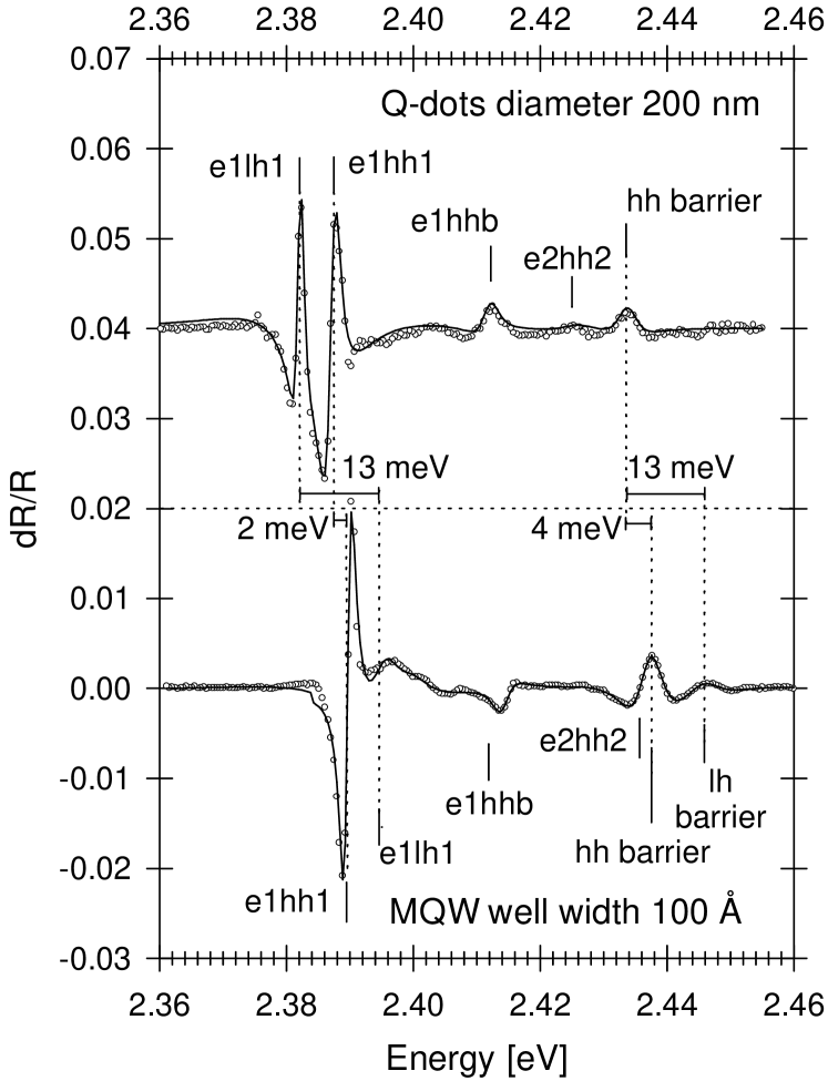
The Q-dot spectrum is shifted vertically by 0.04 units for clarity. We use only the in-phase components of to represent the spectra (in all figures) because the 90∘ out-of-phase components are featureless. This is to be expected since, firstly, the sample is thin compared to the wavelength of the probe light and, secondly, the modulation period is very long compared with the time-scales of the relaxation processes in the samples. Both BPR spectra in figure 3 have the same signal to noise ratio and order of magnitude, which makes it easy to compare them. This is not the case for the unmodulated reflectivity spectra, which for the Q-dots are a factor of ten weaker (and show a different non-excitonic background) than for the MQWs due to the diffraction of the probe light by the Q-dot pattern. Therefore, BPR is a better tool than reflectivity for the study of the nanofabricated samples. In the figure the open circles are the measured values and the full curves are the fits to the spectra. The arrows above and below the spectra mark the fitted energy positions of the transitions in the Q-dot spectrum and the MQW spectrum respectively; the fitted positions of the ZnTe buffer signal are not indicated. The spectrum of the MQW sample was fitted with seven oscillators. We used third-derivative lineshapes (equation (4)) for the ZnTe buffer transition and the light-hole and heavy-hole barrier transitions denoted as hh barrier and lh barrier respectively. First derivatives with respect to energy position of a complex Lorentzian lineshape (equation (3)) were used for the four quantum well related transitions. Three of these can be assigned easily:
these are the lowest quantum well heavy-hole (e1hh1) and light-hole (e1lh1) excitons and the second allowed heavy-hole excitonic transition (e2hh2). In assigning the fourth quantum well related transition, the magnetic field splitting in the Faraday geometry of the and the components of the signal provides useful evidence. This splitting is comparable to the splitting of the heavy-hole barrier exciton, indicating that the signal corresponds to a heavy-hole related transition which may either be a forbidden transition involving the first electron state and a high-index heavy-hole state of the quantum well (probably e1hh3) or an indirect transition between a quantum well electron state and the heavy-hole barrier state. Our preliminary conclusion is that the signal corresponds to the spatially-indirect well-to-barrier transition (e1hhb) since a signal of this type has been observed in a Cd0.97Mn0.03Te/CdTe MQW sample of similar structure and similar confinement situation by low-temperature photoluminescence excitation experiments [57]. The spectrum of the Q-dot sample was fitted with six oscillators, again using first-derivative lineshapes for the four quantum well related transitions, but now only two third-derivative lineshapes representing only one barrier signal (hh barrier) apart from the ZnTe buffer signal. We do not observe any additional features in the BPR of the Q-dot sample that could be related to additional lateral confinement effects in the dots, confirming that the dot diameter is still in the regime where the Coulomb effects dominate over lateral confinement effects. It is possible to observe lateral confinement effects by photomodulated reflectivity experiments in smaller Q-dots, such as modulation-doped GaAs/Ga1-xAlxAs Q-dots of 60 nm diameter at 77 K [58] and Cd1-xMnxTe/CdTe Q-dots of 30-40 nm even at 300 K [35].
The differences between our spectra can be related to different strain states of the Q-dots and the MQW. The dotted lines in figure 3 correspond to the energies of the lowest quantum well transitions (e1hh1 and e1lh1) and to the barrier transitions (e1hh barrier and e1lh barrier). The solid horizontal bars on the horizontal dotted line indicate the shifts of these transitions before and after the nanofabrication process. We find that these shifts are qualitatively in agreement with our simple considerations of the strain shifts for light-hole and heavy-hole excitonic transitions between the two strain situations of the sample strained to the ZnTe buffer for the MQW and the sample strained to the Zn0.93Mn0.07Te barrier for the Q-dot sample. The above discussion of the strain state of the samples predicts a strain shift of the light-hole transitions of 21 meV. In the
analysis of the spectra, we find a shift of 13 meV for the light-hole transitions, whilst for the heavy-hole transitions we predict a shift of 8 meV and observe shifts of 2 meV and 4 meV. Similar behaviour is observed in the other specimens and can be explained fully on the assumption of two well-defined strain states for the two series of samples, as we now show.
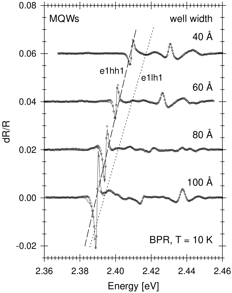
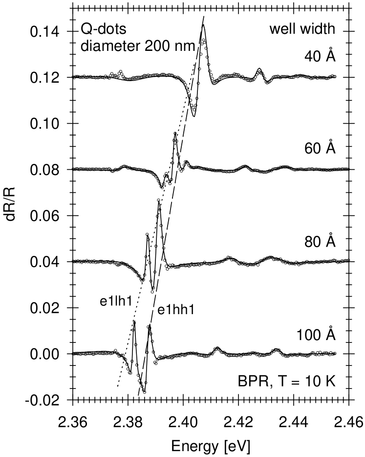
Figures 4 and 5 display the measured and fitted spectra of the series of MQW samples and of the series of Q-dot samples. The spectra are shifted vertically for clarity and are arranged in order of increasing quantum well width from top to bottom. Again, the open circles are the measured values and the full curves are the fits. In each figure, a dotted line and a broken line indicate the change of the energy position of the e1lh1 transition and the e1hh1 transition respectively. The fits of the spectra of the MQW and the Q-dots with quantum well width of 80 Å were the same as described for the corresponding samples of 100 Å quantum well width, that is, seven oscillators for the MQW spectrum and six for the Q-dot spectrum. In the fits of the four spectra of the 40 Å and the 60 Å MQW and Q-dot samples we have not included an oscillator for a e2hh2 transition, thus leaving just six and five oscillators respectively to describe the experimental spectra. In figure 5, the spectrum of the Q-dot sample with 60 Å quantum well width shows two additional features which are situated at the energy positions of the e1hh1 and the e1lh1 transition of the corresponding MQW sample (these features are difficult to discern on the scale of figure 5). These suggest that we have not etched through the whole heterostructure and that the lowest quantum well is still intact. To account for this in the fitting, we have included two more oscillators, fixed at the energy positions already determined for the e1lh1 and e1hh1 transitions of the MQW sample. We now focus on the behaviour of the lowest energy excitonic transitions in the quantum wells, i.e., e1hh1 and e1lh1 and relate this behaviour to the strain state of the sample. For the MQW samples we expect from the potential situation shown in the centre of figure 2 that the e1hh1 transition is lower than the e1lh1 transition and that, with increasing well width, the splitting between the two transitions decreases because the excitons become less sensitive to the strain-splitting of the barrier (the changes in the quantum confinement with well width are less significant than the strain effects in this system). This behaviour can be clearly seen in the spectra in figure 4 as indicated by the convergence of the broken and dotted line.
From the potential situation for the Q-dots depicted on the right of figure 2, we conclude that, in the Q-dots, the e1lh1 and the e1hh1 transition will behave in the opposite way to that described for the MQWs. This agrees well with the behaviour displayed in figure 5: the e1lh1 transition is lowest in energy in the wells of the Q-dots and the splitting between the e1hh1 and e1lh1 transitions increases as the quantum well width increases, that is, as the lowest quantum well transitions become increasingly like those in a strained ZnTe layer. Another interesting aspect is that in the spectra of the Q-dots, we observe an enhancement of the intensity of the e1lh1 transition compared to the e1hh1 transition, which is quite significant for the Q-dot samples of well width 80 Å and 100 Å where the intensity ratio ranges from 1:3 to 1:1. A similar effect was observed in GaAs/Ga0.7Al0.3As quantum dots with diameters of 500 nm, 400 nm and 230 nm and was explained by matrix element effects [27] as follows. The intensity of a transition is, in a first approximation, proportional to the square of the electric dipole matrix element:
| (6) |
where and are the conduction and valence band states respectively and is the electric dipole operator. Making use of the degeneracy in in the absence of a magnetic field, the following expressions for the conduction band state and the heavy-hole and light-hole valence band states in the representation hold [59]:
| (7) | ||||
For an epitaxially grown heterostructure, the probe light is normally incident parallel to the growth direction , thus the dipole operator only has components in the plane, leading to an intensity ratio of 1:3 between the lowest-energy light-hole and heavy-hole transitions. In the case of quantum dots, the probe light can penetrate into the sample via the sidewalls, thus having a component of the dipole moment in the -direction which, from equation (7), increases the intensity of the light-hole transition. (Note that in figure 7 the intensity ratio appears to decrease with the well width and the two transitions approach each other, indicating that matrix element effects can only explain qualitatively the behaviour of the intensity ratio; however, the present experimental evidence is insufficient to draw firm conclusions.)
To verify the proposed model for the strain states of the samples quantitatively, we have carried out calculations of the energies of the observed transitions in each case. Comparisons of the transition energies obtained from the fitting of the spectra with the results of the calculations are shown in figures 6 and 7.
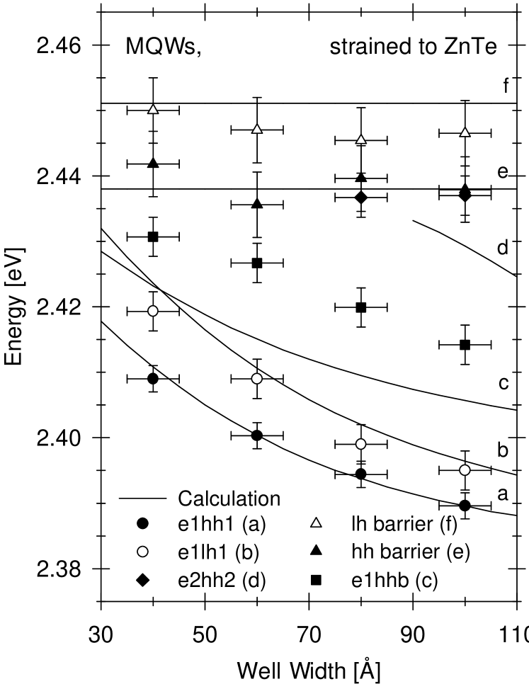
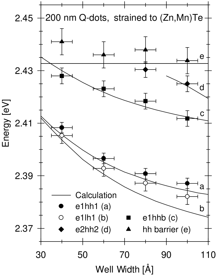
The full curves in figure 6 are calculated assuming a potential profile where the sample is strained to the ZnTe lattice constant (figure 2, centre). The two horizontal lines indicate the hh barrier and lh barrier transitions. The other lines follow the calculated quantum well width dependences for the e2hh2, e1hh1 and e1lh1 transitions and for the e1hhb transition. The dependence on quantum well width of the e2hh2 transition was only calculated for wells wider than 85 Å, for which the second electron state is confined and our transfer matrix method is applicable. The calculated transition energies of the e1hhb do not include a binding energy contribution. This contribution should only lead to a reduction of the calculated value by a few meV because it is a spatially-indirect transition. The error bars on the experimental values are the fitted linewidths of the transitions (along the energy axis) and a 5 Å error bar on the well width axis representing a possible two-monolayer deviation from the nominal quantum well width. The agreement between the calculated values and the fitted values for the MQWs is very good especially for the two barrier transitions and the two lowest quantum well transitions, for which the deviations are within the experimental error bars. The agreement is not as good for the e2hh2 transition and the e1hhb transition, but the calculations show the same trend as the data. Figure 7 shows the results for the Q-dot samples; on this figure, the error bars were determined in the same way as for Figure 6. We do not observe an increased linewidth for the excitonic transitions in the Q-dots, thus there is no indication from the BPR data for an inhomogeneous strain distribution in the Q-dot pillars. Again, we obtain good agreement between theory and experiment. There are two trends as a function of quantum well width which need to be considered. Firstly, the experimental values for the barrier transition are slightly higher than the calculated values for the three wider quantum wells whereas in the case of the MQWs we obtained very good agreement for the three samples. Secondly, the deviation of the experimental results from the calculated dependence increases with increasing quantum well width for the e1hh1 and especially for the e1lh1 transition. The experimental data lie above the calculated energies and the e1lh1-e1hh1 splitting is less than calculated. These trends can be understood assuming that the Q-dots are more or less freestanding, thus the actual lattice constant in the structure approaches an intermediate value of the ZnTe lattice constant and Zn0.93Mn0.07Te lattice constant weighted by the overall thickness of the corresponding layers in the dot pillar:
| (8) |
where and are the overall thicknesses of the respective materials, and are the equilibrium lattice constants of the ZnTe well material and the Zn0.93Mn0.07Te barrier material at the measurement temperature and and . Because the depth of etching into the ZnTe buffer is uncertain, the exact height of the dots is not known and it is difficult to estimate the overall thicknesses in the Q-dot pillars. We therefore replace the thicknesses in equation (8) by the thicknesses of an individual well and barrier, ignoring the role of the buffer layer. Since it is likely that we have not etched deep into the ZnTe buffer layer (as is indicated by the additional features corresponding to signals from an unetched well in the case of the Q-dot sample with 60 Å well width), this is justified. We thus obtain and ; a small value of indicates that approaches , so that this calculation confirms those Q-dot samples with narrow quantum wells are described well by the potential situation assumed in the calculation of the transition energies. For the Q-dot samples with wider wells the potential situation will be of an intermediate type between the two strain states described in figure 2. Again, it should be noted that the actual profiles of the electron and the light-hole and heavy-hole potentials do not change, but are only shifted on an absolute energy scale, varying between the two limits given by the potential situations depicted in the centre and on the right side of figure 2.
We can summarize the experimental results in the following way: the MQW samples are to a good approximation strained to the ZnTe lattice constant whereas the pillars in the Q-dot samples are more or less freestanding, which can be understood by considering the structure of our samples. Similar results have been obtained for nanostructures prepared from other material systems. For example, a strain relaxation has been observed by photomodulated reflectivity in quantum wires with wire widths between 15 nm and 500 nm etched by RIE on a p+-Si/Si0.8Ge0.2 heterostructure [30] or by x-ray diffraction in quantum dots etched from Si1-xGex epilayers with and on a Si-substrate where the pillars were etched through the epilayer into the Si-buffer layer [25]. In the III-V materials, quantum dots of diameter between 230 nm and 500 nm were prepared by RIE from a GaAs/Ga0.7Al0.3As superlattice on a GaAs-substrate an increasing strain relaxation with decreasing dot diameter was observed [27] by photomodulated reflectivity. Finally, in a quantum wire sample with wire width of 145 nm prepared from a InAs/GaAs superlattice on a GaAs substrate, the superlattice structure in the individual wires turned out to be partially relaxed [24].
5 Conclusions
We have prepared large-area high-density patterns of quantum dots with a diameter of 200 nm from a series of four Zn0.93Mn0.07Te/ZnTe multiple quantum well structures of different well widths (40 Å, 60 Å, 80 Å and 100 Å) by electron beam lithography followed by ion beam etching with Ar+ ions. Examination under a scanning electron microscope reveals that the patterns are very homogeneous and have a ratio of dot area to etched area of 1:3. The individual dot pillars have inclined sidewalls with an inclination angle of about 25∘. We have performed below-bandgap photomodulated reflectivity experiments on the series of quantum dot samples and, for comparison, on the series of parent heterostructures. An analysis of the spectra gives the following results. Firstly, we do not see additional confinement effects due to the reduction of the dimensionality from two dimensions to zero dimensions. Secondly, we observe an increasing oscillator strength for the light-hole exciton in the quantum dots. A possible explanation is that the probe light can penetrate into the sidewalls of the quantum dot pillars and can thus induce an electric dipole moment parallel to the growth direction of the heterostructure. This results in an increased matrix element for the light-hole exciton whereas the matrix element of the heavy-hole exciton is not changed. Thirdly, the main changes in the excitonic energies as a consequence of the nanofabrication process are due to a strain relaxation in the quantum dots. We have compared the energy positions of the excitonic transitions obtained by fitting the lineshapes of the experimental spectra with the results of model calculations based on a one-dimensional transfer matrix method followed by an excitonic binding energy calculation. These calculations confirm that the quantum dots are freestanding whereas the original heterostructures are to a good approximation strained to the ZnTe buffer.
Our analysis also shows that below-bandgap photomodulated reflectivity, like conventional photomodulated reflectivity, is a powerful tool to study the effects of nanostructure fabrication on semiconductor structures. In this context, it should be noted that modifications due to the fabrication process can already be observed for structural dimensions larger than those for which additional confinement effects occur. It is therefore of great importance to study nanostructures in this intermediate size regime because a fundamental understanding of the smaller structures will only be attained if a separation of the macroscopic effects (strain relaxation, damage) and the additional confinement effects is possible.
In the future, the effects of the nanostructure fabrication on these samples will be investigated via magneto-optic experiments which make use of the unique magnetic properties of dilute magnetic semiconductors. The changes induced by the strain relaxation in the quantum dots offer interesting possibilities in this context. For example, the photoluminescence of the quantum dot samples has light-hole character in the absence of a magnetic field whereas the photoluminescence of the heterostructures has heavy-hole character. By applying a magnetic field, the character of the photoluminescence in the quantum dots can be changed from light-hole to heavy-hole due to fact that the magnetic field splitting of the heavy holes is greater than that of the light holes.
Acknowledgements
We thank J. J. Davies for a careful reading of the manuscript. The support of the Engineering and Physical Sciences Research Council of the UK under contracts GR/H 57356 and H 93774 is gratefully acknowledged. P. J. Klar thanks the University of East Anglia for the provision of a research studentship. T. Henning is grateful to the Deutscher Akademischer Austauschdienst for a research student grant within the framework of the HSP II scheme. We are also grateful to the Swedish Nanometer Laboratory for the possibilty to use their facilities for the preparation of the Q-dot samples.
References
- [1] Goede O and Heimbrodt W 1988 phys. stat. sol. (b) 146 11
- [2] Furdyna J K 1988 J. Appl. Phys. 64 R29
- [3] Fatah J M, Piorek T, Harrison P, Stirner T and Hagston W E 1994 Phys. Rev. B 49 10341
- [4] Grieshaber W, Haury A, Cibert J, Merle d’Aubigné Y and Wasiela A 1996 Phys. Rev. B 53 4891
- [5] Gaj J, Grieshaber W, Bodin-Deshayes C, Cibert J, Feuillet G, Merle d’Aubigné Y and Wasiela A 1994 Phys. Rev. B 50 5512
- [6] Wolverson D, Railson S V, Halsall M P, Davies J J, Ashenford D E and Lunn B 1995 Semicond. Sci. Technol. 10 1475
- [7] Ekimov A I, Efros A L and Onushchenko A A 1985 Solid State Commun. 56 921
- [8] Sandroff C J, Harbison J B, Ramesh R, Andrejco M J, Hegde M S, Hwang D M , Chang C C and Vogel E M 1989 Science 24 391
- [9] Parthier L, Wissmann H and von Ortenberg M 1996 J. Cryst. Growth 159 99
- [10] Arakawa Y, Nagamune Y, Nishioka M and Tsukamoto S 1993 Semicond. Sci. Technol. 8 1082
- [11] Mariette H, Brinkmann D, Fishman G, Gourgon C, Dang L S and Löffler A 1996 J. Cryst. Growth 159 418
- [12] Pfeiffer L, West K W, Stormer H L, Eisenstein J P, Baldwin K W, Gershoni D and Spector J 1990 Appl. Phys. Lett. 56 1697
- [13] Yater J A, Plaut A S, Kash K, Lin P S D, Florez L T, Harbison J P, Das S R and Lebrun L 1995 J. Vac. Sci. Technol. B 13 2284
- [14] Kash K, Mahoney D D, Van der Gaag B P, Gozdz A S, Harbison J B and Florez L T 1990 J. Vac. Sci. Technol. B 10 2030
- [15] Grundmann M, Ledentsov N N, Heitz R, Eckey L, Christen J, Bohrer J, Bimberg D, Rumvimov S S, Werner P, Richter U, Heydenreich J, Ustimov V M, Egorov A Y, Zhukov A E, Kopev P S and Alverov Z I 1995 phys. stat. sol. (b) 188 249
- [16] Leonard D, Krishnamurthy M, Reaves C M, Denbaars S P and Petroff P M 1993 Appl. Phys. Lett. 63 3203
- [17] Dang L S, Gourgon C, Magnea N, Mariette H and Vieu C 1994 Semicond. Sci. Technol. 9 1953
- [18] Bacher G, Illing M, Forchel A, Hommel D, Jobst B and Landwehr G 1995 phys. stat. sol. (b) 187 371
- [19] Illing M, Bacher G, Forchel A, Waag A, Litz T and Landwehr G 1994 J. Cryst. Growth 138 638
- [20] Sotomayor Torres C M, Smart A P, Foad M A and Wilkinson C D W 1992 Solid State Phys. 32 265
- [21] Foad M A, Wilkinson C D W, Dunscomb C and Williams R H 1992 Appl. Phys. Lett. 60 2531
- [22] Kash K 1990 J. Lumin. 46 69
- [23] Bryant G W 1988 Phys. Rev. B 37 8763
- [24] Holý V, Tapfer L, Koppensteiner E, Bauer G, Lage H, Brandt O and Ploog K 1993 Appl. Phys. Lett. 63 3140
- [25] van der Sluis P, Verheijen M J and Haisma J 1994 Appl. Phys. Lett. 64 3605
- [26] Holý V, Darhuber A A, Bauer G, Wang P D, Song Y D, Sotomayor C M and Holland M C 1995 Phys. Rev. B 52 8348
- [27] Qiang H, Pollak F H, Tang Y S, Wang P D and Sotomayor Torres C M 1994 Appl. Phys. Lett. 64 2830
- [28] Tang Y S, Wang P D, Sotomayor Torres C M, Lunn B and Ashenford D E 1995 J. Appl. Phys. 77 6481
- [29] Tang Y S, Sotomayor Torres C M, Kubiak R A, Whall T E, Parker E H C, Presting H and Kibbel H 1995 J. Electronic Mat. 24 99
- [30] Tang Y S, Wilkinson C D W, Sotomayor Torres C M, Smith D W, Whall T E and Parker E H C 1993 Solid State Commun. 85 199
- [31] Mariette H, Gourgon C, Dang L S, Vieu C, Pelekanos N and Rühle W W 1995 Mat. Sci. Forum 182–184 99
- [32] Maille B E, Forchel A, Germann R and Grützmacher D 1989 Appl. Phys. Lett. 54 1552
- [33] Gourgon C, Dang L S, Mariette H, Vieu C and Muller F 1995 Appl. Phys. Lett. 66 1635
- [34] Sotomayor Torres C M, Smart A P, Watt M, Foad M A, Tsutsui K and Wilkinson C D W 1994 J. Electronic Mat. 23 289
- [35] Ribayrol A, Tang Y S, Zhou H P, Coquillat D, Sotomayor Torres C M, Lascaray J P, Lunn B, Ashenford D E, Feuillet G and Cibert J 1996 J. Cryst. Growth 159 434
- [36] Darhuber A A, Straub H, Ferreira S O, Fashinger W, Sitter H, Koppensteiner E, Brunthaler G and Bauer G 1995 Mat. Sci. Forum 182–184 423
- [37] Klar P J,Wolverson D, Davies J J, Lunn B, Ashenford D E and Henning T to be published in the Conf. Proceed. of the ICPS 1996 (Singapore: World Scientific)
- [38] Bhimnathwala H and Borrego J M 1992 Solid State Electronics 35 1503
- [39] Rockwell B, Chandrasekhar H R, Chandrasekhar M, Ramdas A K, Kobayashi M and Gunshor R L 1991 Phys. Rev. B 44 11307
- [40] Klar P J, Townsley C M, Wolverson D, Davies J J, Ashenford D E and Lunn B 1995 Semicond. Sci. Technol. 10 1568
- [41] Klar P J, Wolverson D, Ashenford D E and Lunn B 1996 J. Cryst. Growth 159 528
- [42] Somekh S and Casey Jr H C 1977 Appl. Optics 16 126
- [43] Tsutsui K, Hu E L, Wilkinson C D W 1993 Jpn. J. Appl. Phys. 32 6233
- [44] Seraphin B O and Bottka N 1966 Phys. Rev. 145 628
- [45] Aspnes D E 1973 Surf. Sci. 37 418
- [46] Bir G L and Pikus G E 1974 Symmetry and Strain-induced Effects in Semiconductors (New York: Wiley)
- [47] Hilton P, Goodwin J, Harrison P and Hagston W E 1992 J. Phys. A: Math. Gen. 25 2395
- [48] Hilton C P, Hagston W E and Nicholls J E 1992 J. Phys. A: Math. Gen. 25 5365
- [49] Mathieu H, Lefebvre P and Cristol P 1992 Phys. Rev. B 46 4092
- [50] Cheng H H, Nicholas R J, Lawless M J, Ashenford D E and Lunn B 1995 Phys. Rev. B 52 5269
- [51] van der Walle C G 1989 Phys. Rev. B 39 1871
- [52] Leiderer H, Jahn G, Silberbauer M, Kuhn W, Wagner H P, Limmer W and Gebhardt W 1991 J. Appl. Phys. 70 398
- [53] Lee Y R, Ramdas A K and Aggarwal R L 1986 Proc. 18th Int. Conf. on Physics of Semiconductors, Stockholm.
- [54] Twardowski A 1982 Phys. Lett. A 94 103
- [55] Twardowski A, Swiderski P, von Ortenberg M and Pauthenet R 1984 Solid State Commun. 50 509
- [56] Mertins H-C, Gumlich H-E and Jung Ch 1993 Semicond. Sci. Technol. 8 1634.
- [57] Chen P, Nicholls J E, Hogg J H C, Stirner T, Hagston W E, Lunn B and Ashenford D E 1995 Phys. Rev. B 52 4732
- [58] Gumbs G, Huang D, Qiang H, Pollak F H, Wang P D, Sotomayor Torres C M and Holland M C 1994 Phys. Rev. B 50 10962
- [59] Bastard G 1988 Wave mechanics applied to semiconductor heterostructures (Les Ulis Cedex: les éditions de physique)