Influence of
Quantum Fluctuations on Phase Coherent Andreev Tunneling
Andrea Huck1 F.W.J. Hekking2 and Bernhard Kramer11 I. Institut für Theoretische Physik, Jungiusstrasse 9,
D-20355 Hamburg, Germany
2Cavendish Laboratory, University of Cambridge,
Madingley Road, Cambridge CB3 OHE, United Kingdom
Abstract
We study the subgap transport properties of a small capacitance
normal metal-superconductor tunnel junction coupled to an
external electromagnetic environment.
Mesoscopic interference between the electrons in the normal metal
strongly enhances the subgap conductance with decreasing bias voltage.
On the other hand, quantum fluctuations of the environment
destroy electronic phase coherence and suppress the subgap conductance
at low bias (Coulomb blockade).
The competition between charging effects and mesoscopic interference
leads to a non-monotonic dependence of the differential subgap
conductance on the applied bias voltage. This feature is pronounced,
even if the coupling to the environment
is weak and the charging energy is small.
pacs:
PACS numbers:74.50.+r, 72.10.Fk
Charge transport through a tunnel barrier between a normal metal (N)
and a superconductor (S) is a widely investigated topic [1].
At energies much smaller than the superconducting gap ,
tunneling of single particles is exponentially suppressed.
Under these conditions,
charge transport through an N-S interface is dominated by
Andreev reflection [2]. If the normal metal and the
superconductor are separated by a low transparency tunnel barrier,
two-electron tunneling [3] determines the subgap conductance.
Recently,
there has been much interest in the subgap properties of mesoscopic
N-S junctions [4, 5].
The dependence of the subgap conductance of a tunnel junction on
temperature or applied bias voltage can be very different, depending
on the precise lay-out of the system under consideration.
If, for instance, we consider a tunnel junction between a
superconductor and a
thin metallic film at low temperatures, electrons move
phase coherently in N and undergo multiple elastic scattering
events by impurities or rough sample boundaries.
As a consequence, they will be scattered back to the junction
interface several times, where they attempt to tunnel into S.
Two-electron tunneling involves two almost time reversed
electrons. Therefore, the phase of the two-electron tunneling amplitude
is not randomized by elastic scattering and the amplitudes
for various tunneling
attempts add up coherently. This strongly enhances the subgap conductance
at low bias voltages [6, 7].
On the other hand, in mesoscopic N-S tunnel junctions with
a small junction capacitance , charging effects[8] become important.
In order to tunnel, the two electrons should overcome the characteristic
Coulomb interaction energy . This will strongly suppress the subgap conductance [9, 10] at low temperatures and bias
voltages , a phenomenon known as Coulomb blockade of
two-electron tunneling.
In the present paper we will discuss the influence of the competition between
charging and interference effects on the subgap conductance of a
single N-S tunnel junction. Charging effects in a single junction are
conveniently described using the so-called electromagnetic environment model
[11]. In this model, electron tunneling is studied
in the presence of
quantum phase fluctuations due to the Johnson-Nyquist noise of the
external circuit, seen by the junction.
In the simplest case, this circuit
consists of a capacitor (i.e., the junction capacitance) and an
external series resistor ,
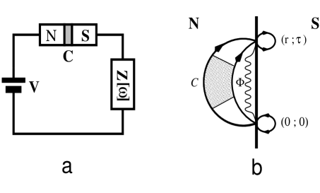
see Fig. 1a.
The influence of such an environment on the subgap conductance
of N-S junctions
has been studied before [12], but without considering
mesoscopic interference.
We will show how interference effects are destroyed as
the series resistance , which determines the coupling to the
environment, is increased. If the charging energy is smaller than
the superconducting gap,
the competition between
quantum fluctuations and mesoscopic interference leads to a
non-monotonic dependence of the differential subgap conductance on
bias voltage, even for weak coupling.
The system shown in Fig. 1a
can be described by the Hamiltonian .
Here, denotes the unperturbed Hamiltonian,
, where
and describe the disordered normal metal and the
superconductor, respectively.
The electromagnetic environment is described by the usual
bosonic Caldeira-Leggett[13] Hamiltonian .
The tunnel Hamiltonian transfers electrons between N and S
and couples the electrons to the environment; it will be treated
perturbatively.
In the interaction picture takes the form
(1)
(2)
Here, is a fermionic field operator for an electron
with and spin ;
is the amplitude to tunnel from a point in
N to in S, and the applied
bias voltage. The phase operator
describes the voltage fluctuations at the tunnel junction, induced
by the electromagnetic environment. Its dynamics is governed by
.
From an expansion
in up to fourth order,
using standard imaginary-time techniques,
one obtains the following expression for the subgap current:
(4)
where and the
analytical continuation for the bosonic Matsubara frequencies
has to be performed.
In order to obtain (4), we assumed tunneling
to occur between neighboring points on the
barrier B, located at ; correspondingly we put
.
The amplitude can be expressed in terms of the normal state
conductance of the tunnel barrier, . Here
is the quantum resistance, the density of states at the Fermi level
and the Fermi velocity; is the area of the barrier surface.
Furthermore, we introduced the four-point correlator
describing the propagation of two electrons for , as well as a
four-point phase correlator
related to the voltage fluctuations.
The averages are taken with respect to
, , and , respectively; in addition the
correlator is to be averaged over disorder.
Further simplification can be achieved following Ref.[6].
At energies much smaller than the gap , two electrons propagate
coherently through N over distances
of the order
, much
larger than the corresponding length in S
( is the diffusion constant and the phase
breaking time); moreover,
the lifetime
of a quasiparticle in S in the intermediate state is negligibly small.
Therefore, we have
in Eq. (4).
The dominant contribution to the subgap current can now be written as
(5)
(6)
The integrand of Eq. (6) is depicted diagrammatically in
Fig. 1b. We see
two electrons tunneling from S to N at initial position and time (0;0)
thereby
interacting with the environment.
The electrons propagate through N to position , where they
arrive at time ; their propagation is described by the
disorder averaged two-particle correlator (Cooperon),
.
Then they tunnel back into S, interacting once more with the
environment.
The wavy line in Fig. 1b denotes the phase correlator
, where we choose
according to the electromagnetic environment model [11]:
(7)
(8)
Here is
the total impedance seen by
the junction.
Upon performing the analytic continuation in Eq. (6)
the pair tunneling current finally is found to be
(9)
(10)
The function
is the spatial fourier transform of the real part of
the diffusion propagator .
The probability to emit or absorb a photon with
frequency during tunneling is defined as
(11)
where can be obtained from Eq. (8) by putting
for .
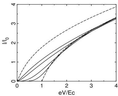
As an example, we will study the Andreev current (10) of a N-S
tunnel junction,
consisting of a quasi one-dimensional (1D)
normal metal wire in contact with a superconductor via a tunnel barrier
with dimensions much smaller then .
For a quasi 1D wire with cross section , we have
in Eq. (10).
The junction has a capacitance and is
embedded in a purely resistive environment
. The total impedance is thus given by
.
However, the calculation of can only be performed numerically
in this case [14]. Therefore,
in order to proceed analytically, we will use the
approximation ,
which has the correct zero-frequency limit .
The cut-off frequency is chosen to be , such that
the approximated impedance also gives the correct
phase correlation function
in the limit of short times. In particular, this guarantees that this
approximation yields
the correct behavior for , namely the
complete suppression of tunneling for .
At zero temperature the phase correlation function is readily found to be
; its fourier transform
(11) yields the probability distribution
(12)
The negative part of the spectrum is truncated, since at
photons can only be emitted.
The power can be interpreted as a parameter
determining the coupling strength between the
electronic phase and the environment.
For the non-interacting system,
, the subgap conductance is proportional to the
”coherence resistance” [6], where
denotes the conductivity of the wire.
In the limit of strong coupling, , a gap
appears in the I-V curve below .
We will focus on the case of small charging energies .
For a finite coupling and
finite phase coherence time [15], two regimes exist
(see Fig. 2):
(i)
For very small voltages ,
interference is cut off by
and the I-V curve shows a power law
behavior .
This is what one would expect for
noninterfering electrons.
(ii) For higher voltages
the coherence length is voltage dependent
and the I-V characteristic changes: .
Remarkably, if
and , suppression
of the current by charging effects and
enhancement by interference cancel each other exactly
at voltages below , such that the
I-V curve is linear.
For values of larger than the ”critical” coupling ,
the power is always larger than one and a Coulomb gap starts to evolve
with increasing .
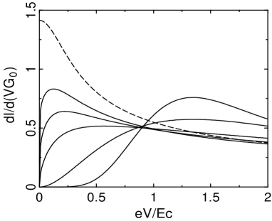
The differential conductance is strongly suppressed at
for arbitrary .
The zero bias peak, which is the
fingerprint of phase coherent Andreev tunneling, is destroyed by charging
effects.
Instead, the differential conductance will display a peak at finite bias
(Fig. 3).
Increasing the voltage on the one hand lifts
the Coulomb blockade, but on the other hand decreases the coherence length.
If , the maximum
in the differential conductance
appears at a bias
and will shift to zero bias
for . The coupling to the quantum fluctuations
of the environment is too weak
to fully destroy phase coherence. Therefore coherent pair tunneling is
blocked
only at voltages below , where interference is cut off.
For , the coupling is strong enough for charging effects
to dominate the behavior. The conductance is suppressed in the entire
voltage regime below by quantum fluctuations,
which makes superfluous as
a cutoff for the divergence of at zero bias.
The maximum appears at and shifts towards
as is increased.
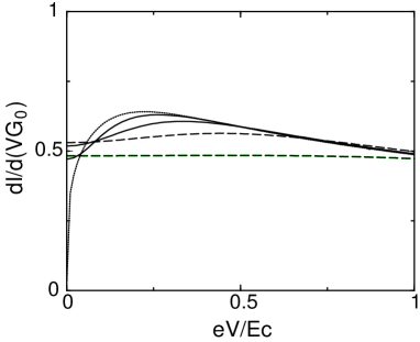
At finite temperatures, the electrons
can gain energy by absorbing environmental modes.
Therefore,
the Coulomb blockade is gradually lifted
with increasing temperature.
The probability distribution at small energies
can be calculated analytically, following [16].
In the long time limit, the phase correlator reads
.
From (11) we find
(13)
For low temperatures one easily calculates
the zero bias
differential conductance
with the help of (13).
For we find
,
whereas for
.
In order to determine away from zero bias, the function
should be calculated for arbitrary . For nonzero temperatures, this can only
be done numerically. Qualitatively, one expects the Coulomb blockade
to be lifted if
for weak coupling, , whereas for
thermal smearing becomes relevant at temperatures .
As an example, the
differential conductance as a function of bias voltage is sketched in
Fig. 4 for at various temperatures .
Acknowledgments. The authors would like to thank
D. Averin, R. Fazio,
A. van Otterlo, and
M. Sassetti for useful discussions.
The financial support of the European Union
(Contract
ERB-CHBI-CT941764) is gratefully acknowledged.
Part of this work was done at the ISI Torino and the ICTP Trieste.
REFERENCES
[1]
M. Tinkham, Introduction to Superconductivity (McGraw-Hill, New York,
2nd ed., 1996).
[3]
J.W. Wilkins in Tunneling Phenomena in Solids, edited by
E. Burstein and S. Lundqvist (Plenum, New York, 1969), p. 333.
[4]Mesoscopic Superconductivity, edited by
F.W.J. Hekking, G. Schön, and D.V. Averin, Physica B 203 Nos.
3 & 4 (1994).
[5] C.W.J. Beenakker in Mesoscopic Quantum
Physics, edited by E. Akkermans et al. (North-Holland, Amsterdam, 1995).
[6]
F.W.J. Hekking and Yu.V. Nazarov, Phys. Rev. Lett. 71, 1625
(1993); Phys. Rev. B 49, 6847 (1994).
[7]
H. Pothier et al., Phys. Rev. Lett.
73, 2488 (1994).
[8]
D.V. Averin, K.K. Likharev, in Mesoscopic Phenomena in Solids,
edited by B. L. Altshuler,
P. A. Lee, and R. A. Webb (North-Holland, Amsterdam, 1991);
G.L. Ingold, Yu.V. Nazarov in Single Charge Tunneling,
edited by H. Grabert and M.H. Devoret, (Plenum, New York, 1992).
[9]
T.M. Eiles, J.M. Martinis and M.H. Devoret, Phys. Rev. Lett. 70,
1862 (1993);
J.M. Hergenrother, M.T. Tuominen and M. Tinkham, Phys. Rev. Lett. 72,
1742 (1994).
[10]
F.W.J. Hekking et al., Phys. Rev. Lett.
70, 4138 (1993);
G. Schön and A. Zaikin, Europhys. Lett. 26, 695 (1994).
[11]M.H. Devoret et al., Phys. Rev. Lett. 64, 1824
(1990); S.M. Girvin et al., Phys. Rev. Lett. 64, 3183 (1990).
[12]
J.J. Hesse and G. Diener in Ref.[4];
A. Bardas, Solid State Commun. 103, 113 (1997).
[13]
A.O. Caldeira and A.J. Leggett, Ann. Phys. (NY) 149, 374 (1983).
[14] G. Falci, V. Bubanja, and G. Schön,
Europhys. Lett. 16, 109 (1991); Z. Phys. B 85, 451 (1991).
[15] In typical experiments, like
Ref. [7], is relatively large
( 10 mK)
at the lowest temperatures.
[16] G.-L. Ingold, H. Grabert, and U. Eberhardt,
Phys. Rev. B 50, 395 (1994).
FIG. 1.: (a) Single N-S junction with a capacitance
coupled to an external circuit with an impedance and a
voltage source. (b) Two electrons propagating
coherently in a disordered normal metal
as a cooperon (half-moon) coupled to the
electromagnetic environment by the phase correlator
(wavy line). The upper loop describes two electrons
which immediately form a Cooper pair after entering the
superconductor; the lower loop describes
the corresponding time-reversed process.FIG. 2.: Andreev current in units of
for and .
Curves from top to bottom correspond to (dashed line),
(solid lines)
and (dashed line).FIG. 3.: Differential conductance in units of
for and .
The maximum evolves to the right as is increased from
(dashed line), taking
(solid lines).FIG. 4.: Sketch of differential conductance for .
From top to bottom, temperature increases: (dotted line),
(solid lines), and (dashed lines).