Enhanced shot noise in resonant tunneling: theory and experiment
Abstract
We show that shot noise in a resonant tunneling diode biased in the negative differential resistance regions of the I-V characteristic is enhanced with respect to “full” shot noise. We provide experimental results showing a Fano factor up to 6.6, and show that it is a dramatic effect caused by electron-electron interaction through Coulomb force, enhanced by the particular shape of the density of states in the well. We also present numerical results from the proposed theory, which are in agreement with the experiment, demonstrating that the model accounts for the relevant physics involved in the phenomenon.
pacs:
PACS numbers: 73.40.Gk, 71.20.-b, 73.20.Dx, 72.70.+mDeviations from the purely poissonian shot noise (the so-called “full” shot noise) in mesoscopic devices and resonant tunneling structures have been the subject of growing interest in the last decade. [2, 3, 4, 5, 6, 7, 8, 9, 10, 11, 12, 13] The main reason is that noise is a very sensitive probe of electron-electron interaction, [14] both due to the Pauli principle and to Coulomb force, and provides information not obtainable from DC and AC characterization; furthermore, noise depends strongly on the details of device structure, so that the capability of modeling it in nanoscale devices implies and requires a deep understanding of the collective transport mechanisms of electrons.
Almost all published theoretical and experimental studies have focussed on the suppression of shot noise due to negative correlation between current pulses caused by single electrons traversing the device. Such correlation may be introduced by Pauli exclusion, which limits the density of electrons in phase space, and/or by Coulomb repulsion, depending on the details of the structure and on the dominant transport mechanism,[7, 8, 9, 10] and make the pulse distribution sub-poissonian, leading to suppressed shot noise.
In particular, for the case of resonant tunneling structures, several theoretical and experimental studies have appeared in the literature, [3, 4, 5, 6, 7, 8, 9, 10, 11, 12, 13] assessing that the power spectral density of the noise current in such devices may be suppressed down to half the “full” shot noise value , i.e., that associated to a purely poissonian process.
In this Letter, we propose a theoretical model and show experimental evidence of the opposite behavior, that is of enhanced shot noise with respect to , which is to be expected in resonant tunneling structures biased in the negative differential resistance region of the - characteristic.
We shall show that in such condition Coulomb interaction and the shape of the density of states in the well introduce positive correlation between consecutive current pulses, leading to a super-poissonian pulse distribution, which implies a super-poissonian shot noise.
First, we shall show an intuitive physical picture of the phenomenon, then we shall express it in terms of a model for transport and noise in generic resonant tunneling structures presented elsewhere [10, 15]. Furthermore, we shall show the experimental results, exhibiting a noise power spectral density almost 6.6 times greater than , and compare it with the results provided by a numerical implementation of our model.
As is well known, the typical I-V characteristic of a resonant tunneling diode is due to the shape of the density of states in the well, which consists of a series of narrow peaks in correspondence with the longitudinal allowed energies in the well: for the GaAs/Al0.36Ga0.64As material system considered here, there is a single narrow peak. In the negative differential resistance region of the I-V characteristic, the peak of the density of states is below the conduction band edge of the cathode: with increasing voltage, the density of states is moved downward, so that fewer states are available for tunneling from the cathode, and the current decreases.
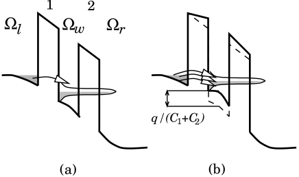
The microscopic mechanism which allows for enhanced shot noise is the following (see Fig. 1): an electron tunneling into the well from the cathode raises the potential energy of the well by an amount , where is the electron charge, and the capacitances between the well region and either contacts; as a consequence, the density of states in the well is shifted upwards by the same amount, with the result that more states are available for successive tunneling events from the cathode, and the probability per unit time that electrons enter the well increases. That means that electrons entering the well are positively correlated, so that enhanced shot noise is to be expected.
For a more analytical derivation we can consider the structure as consisting of three regions , , and , i.e., the left reservoir, the well region, and the right reservoir, respectively, that are only weakly coupled through the two tunneling barriers 1 and 2, as sketched in Fig. 1(a). In addition, we suppose that electron transport is well described in terms of sequential tunneling (which is reasonable, except for the case of temperatures in the millikelvin range): an electron in traverses barrier 1, loses phase coherence and relaxes to a quasi-equilibrium energy distribution in the well region , then traverses barrier 2 and leaves through .
Since confinement is realized only in one direction (that of MBE growth), a state in () is characterized by its longitudinal energy , its transverse wave vector , and its spin , and tunneling can be treated as a transition between levels in different regions [16] in which , and are conserved.
Following Davies et al. [8], we introduce “generation” and “recombination” rates through both barriers: [10] the generation rate is the transition rate from to , i.e., the sum of the probabilities per unit time of having a transition from to given by the Fermi “golden rule” over all pairs of occupied states in and empty states in . Analogously, we define , the recombination rate through barrier 1 (from to ), and , generation and recombination rates through barrier 2.
Since negative differential resistance is obtained at high bias, when the electron flux is one-directional, and can be discarded, while and are:
| (2) | |||||
| (4) | |||||
where , , (), are the longitudinal density of states and the equilibrium occupation factor in (dependent on the quasi Fermi level ), respectively, and is the density of transverse states; is the matrix element for a transition through barrier 1 between states of longitudinal energy : it is obtained in Ref. [15] as , where () is the so-called attempt frequency in and is the tunneling probability of barrier 1; is analogously defined.
As is well known, in the negative resistance region of the - characteristic, the peak of is below the conduction band edge of the left electrode. In such a way, as the voltage is increased, the number of allowed states for a transition from to is reduced, hence the current decreases. Since all electrons relax to lower energy states once they are in the well, it is reasonable to assume that -states with longitudinal energies above the conduction band edge of the left electrode are empty, i.e., correspond to a zero occupation factor (analogously, ). In addition, if we discard size effect in the cathode, we have that if . Therefore we can rewrite and as
| (5) | |||||
| (6) |
where is the occupation factor of , () integrated over the transverse wave vectors , and is the bottom of the conduction band edge in the well.
Let us point out that and depend on the number of electrons in the well region both through the potential energy profile, which is affected by the charge in through the Poisson equation, and through the term in (6) which depends on through the quasi-Fermi level . It is worth noticing that in our case Pauli exclusion has no effect, since practically all possible final states are unoccupied. Following these considerations, and can be obtained as a function of , at a given bias voltage .
The steady state value of satisfies charge conservation in the well, i.e., , and the steady state current is .
Following Ref. [10], it is worth expanding and around and defining the following characteristic times:
| (7) |
Our parameter of choice for studying deviations from full shot noise is the so-called Fano factor , the ratio of the power spectral density of the current noise to the full shot value . From [10] we have, in this case, for ,
| (8) |
From the definition (7), is positive in the first region of the I-V characteristic, when Pauli principle and Coulomb interaction make decreasing with increasing . On the other hand, in the negative differential resistance region, the term which varies the most with increasing N is the longitudinal density of states, which shifts upwards by a factor per electron: since the peak is just below , a slight shift of the peak sensibly increases the integrand in (5), yielding a negative . Note that, while from (8) we see that noise could also diverge if , this cannot physically happen, because the large deviation of with respect to would make the linearization of and not acceptable.
We now focus on a particular structure, on which we have performed noise measurements and numerical simulations following the theory just described. Such structure has been fabricated at the TASC-INFM laboratory in Trieste and has the following layer structure: a Si-doped ( cm-3) 500 nm-thick GaAs buffer layer, an undoped 20 nm-thick GaAs spacer layer to prevent silicon diffusion into the barrier, an undoped 12.4 nm-thick AlGaAs first barrier, an undoped 6.2 nm-thick GaAs quantum well, an undoped 14.1 nm-thick AlGaAs barrier, a 10 nm GaAs spacer layer and a Si-doped 500 nm-thick cap layer. The aluminum mole fraction in both barriers is and the diameter of the mesa defining the single device is about m.
The barriers in our samples are thicker than in most similar resonant-tunneling diodes, for the purpose of reducing the current and, consequently, to increase the differential resistance, in order to obtain the best possible noise match with the measurement amplifiers (available ultra-low-noise amplifiers offer a good performance, with a very small noise figure, for a range of resistance values between a few kiloohms and several megaohms).
We have applied a measurement technique purposedly developed for low-level current noise measurements, based on the careful evaluation of the transimpedance between the device under test and the output of the amplifier. [18] This procedure allows us to measure noise levels that are up to 3 dB below that of the available amplifiers with a maximum error around 10%.
Our usual approach [18] includes also the subtraction of the noise due to the amplifier and other spurious sources, which is evaluated using a substitution impedance, equivalent to that of the device under test with known noise behaviour. For the measurements in the negative differential resistance region, instead, we have evaluated an upper limit for the noise contribution from the amplifier in these particular operating conditions, since it is difficult to sinthesize an appropriate substitution impedance. From experimental and theoretical considerations, we have verified that such limit is always below 3 % of the noise level from the device under test, so that corrections are not necessary. In Fig. 2 the measured current and the Fano factor at the temperature of liquid nitrogen (77 K) are plotted as a function of the applied voltage (the thicker barrier is on the anode side).
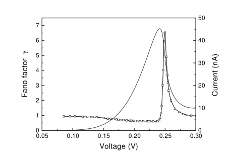
It can be noticed that as the voltage increases, the Fano factor decreases down to about 0.5 (which corresponds to the maximum theoretical suppression [10]), at the voltage corresponding to the current peak is exactly one, then increases again and reaches a peak of 6.6 at the voltage corresponding to the lowest modulus of the negative differential resistance, while, for higher voltages, it rapidly approaches one.
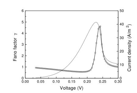
In Fig. 3 we show numerical results for the same structure at 77 K based on the theory discussed before and obtained by considering a relaxation length of 15 nm.[15] As can be seen, there is an almost quantitative agreement between theory and experiment ( the peak experimental current is 45 nA which corresponds to a current density of 23 A/m2): we ascribe most of the difference to the tolerance in the nominal device parameters. All the relevant features of the Fano factor as a function of the applied voltage are reproduced, and can be easily explained in terms of our model.
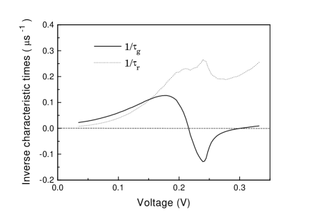
The fact that is maximum at the voltage corresponding to the minimum negative differential resistance of the device is readily justified once we recognize that is practically proportional to [19]. In fact, from Fig. 4 it is clear that varies much more smoothly than with the applied voltage, so that, since and have opposite sign, the modulus of is minimum when approaches . At this point, we simply notice, from (8), that gets larger as approaches , too (and would eventually diverge for ).
Furthermore, from Figs. 3 and 4, and according to [19], we can notice that and tend to infinity at about the same voltage, i.e., the one corresponding to the current peak. Therefore, according to (8), is 1 at the current peak bias, as can be verified from both experiments and calculations (Figs. 2 and 3, respectively).
In conclusion, we have demonstrated experimentally that Coulomb interaction, enhanced by the shape of the density of states in the well, can lead to a dramatic increase of shot noise in resonant tunneling diodes biased in the negative differential resistance region of the I-V characteristic. We have provided a model which leads to good numerical agreement with the experimental data, taking into account all the relevant physics involved in the phenomenon.
This work has been supported by the Ministry for the University and Scientific and Technological Research of Italy, and by the Italian National Research Council (CNR).
REFERENCES
- [1] Fax number: +39-50-568522. e-mail: ianna@pimac2.iet.unipi.it
- [2] G. B. Lesovik, JETP Lett. 49, 592 (1989) (Pis’ma Zh. Eksp. Teor. Fiz. 49, 513 (1989)).
- [3] Y. P. Li, A. Zaslavsky, D. C. Tsui, M. Santos, M. Shayegan, Phys. Rev. B 41, 8388 (1990).
- [4] B. Yurke and G. P. Kochanski, Phys. Rev. B 41, 8184 (1990).
- [5] M. Büttiker, Phys. Rev. Lett. 65, 2901 (1990).
- [6] M. Büttiker, Phys. Rev. B 46, 12485 (1992).
- [7] L. Y. Chen, C. S. Ting, Phys. Rev. B 46, 4717 (1992).
- [8] J. H. Davies, P. Hyldgaard, S. Hershfield, J. W. Wilkins, Phys. Rev. B 46, 9620 (1992).
- [9] E. R. Brown, IEEE Trans. Electron Devices 39, 2686 (1992).
- [10] G. Iannaccone, M. Macucci, B. Pellegrini Phys. Rev. B 55, 4539 (1997).
- [11] H. C. Liu, J. Li, G. C. Aers, C. R. Leavens, and M. Buchanan, Phys. Rev. B 51 5116 (1995).
- [12] P. Ciambrone, M. Macucci, G. Iannaccone, B. Pellegrini, L. Sorba, M. Lazzarino, F. Beltram, Electronics Lett. 31, 503 (1995).
- [13] G. Lombardi, M. Macucci, G. Iannaccone, B. Pellegrini, Proc. of ICNF97 (World Scientific, Singapore), 663 (1997).
- [14] R. Landauer, Physica B 227, 156 (1996).
- [15] G. Iannaccone, B. Pellegrini, Phys. Rev. B 52, 17406 (1995).
- [16] J. Bardeen, Phys. Rev. Lett. 6, 57 (1961).
- [17] G. Iannaccone, B. Pellegrini, Phys. Rev. B 53, 2020 (1996).
- [18] M. Macucci, B. Pellegrini, IEEE Trans. Instr. Meas. 40, 7 (1991).
-
[19]
We just provide a brief argument:
since electrons in the well obey a quasi-equilibrium distribution, we can assume that the currents through each barrier essentially depend on the difference between the quasi-Fermi levels on both sides of the barrier. We therefore choose to leave and fixed, and let only vary. We use the fact that and that depends on , to write
where the last equality comes from (7) and all derivatives are evaluated for .