Nanoscopic Tunneling Contacts on Mesoscopic Multiprobe Conductors
Abstract
We derive Bardeen-like expressions for the transmission probabilities
between two multi-probe mesoscopic conductors coupled by a weak tunneling
contact. We emphasize especially the dual role
of a weak coupling contact as a current source and
sink and analyze the magnetic field symmetry.
In the limit of a point-like tunneling contact the transmission
probability becomes a product of local, partial density of states
of the two mesoscopic conductors. We present expressions for
the partial density of states in terms of functional derivatives
of the scattering matrix with respect to the local potential and in terms
of wave functions. We discuss voltage measurements and resistance measurements
in the transport state of conductors.
We illustrate the theory for the simple case of a scatterer
in an otherwise perfect wire. In particular, we investigate the development
of the Hall-resistance as measured with weak coupling probes.
PACS numbers: 61.16 Ch, 72.10 Fk, 73.20 At
I Introduction
Tunneling from a small metallic tip or from a suitable mesoscopic contact into a sample is a powerful means for the structural analysis of surfaces on an atomic length scale [1]. In the typical arrangement a two-terminal measurement is performed using the tip (contact) as a source and the sample as a current sink. Modeling the tip as a spherical symmetric object (s-wave) and using Bardeen’s approach[2] the current flowing from the tip into the sample was found to be proportional to the local density of states (LDOS) of the surface at the position of the tip[3, 4]. In this article we investigate arrangements in which the sample is so small that the phase coherence length exceeds all sample dimensions. The sample is connected to several contacts, which makes it possible to investigate it in a transport state. In particular, multiterminal resistance measurements become possible. In one interesting configuration two of the contacts of the sample act as current source and sink and the STM (or contact) serves as a voltage probe (see Fig. 1).

Pioneering experiments using such a configuration have been undertaken by Muralt et al.[5] and Kirtley et al.[6] . Theoretically weak coupling contacts to small conductors were considered already by Engquist and Anderson[7] to find the resistance of a scatterer. The discussion of Engquist and Anderson led to Landauer’s result[8] which expresses the resistance of a scatterer in terms of the ratio of its reflection probability and its the transmission probability . Landauer’s derivation makes no appeal to measurement probes, but following Engquist and Anderson subsequent multichannel generalizations of this result by Azbel[9] and Büttiker et al.[10] were also given interpretations as weak coupling measurements by Imry[11]. It was later pointed out that the discussion of Engquist and Anderson is not exact but neglects Friedel-like oscillations, generated by the interference of incident waves reflected at the scatterer[12]. Interest in the multichannel generalization of Azbel faded when it was noticed that it could not account for the magnetic field asymmetry observed in metallic diffusive wires[13]. Furthermore, in mesoscopic physics experiments probes typically are massive and cannot be treated as a weak coupling measurement. A general multiterminal approach which treats all probes on an equal footing was introduced by Büttiker[14]. This approach, which expresses resistances as rational functions of transmission probabilities, also permits a discussion of weak coupling probes. But to our knowledge a detailed investigation of weak coupling probes based on this general approach has not been carried out. Below we will present such an analysis in which the weak coupling probes and the sample are described with one overall scattering matrix.
While the initial experiments by Muralt et al. [5] and Kirtley et al. [6] are difficult to interpret improvements in sample preparation techniques and in low temperature STM will hopefully lead to a resumption of such measurements. In two terminal configurations Friedel oscillations in the equilibrium electron density near steps[15, 16] and in atomic chorals[17] have been observed and there is no principal reason why a similar resolution could not be achieved in the measurement of the transport state. A detailed discussion of potential oscillations near a barrier has been given by Chu and Sorbello[18]. These authors also find a marked difference between the potential measured at the weak coupling probe and the electrostatic potential in the bulk of the sample.
It is the purpose of this work to derive general weak coupling formulae for multiterminal conductors. Of particular interest is a formulation in which the dual role of the weak coupling contact, which can act either as a current injector (or sink) or as a voltage probe, appears in a manifestly reciprocal way. We start from the multiterminal formulation of Ref. [14, 19] which is valid for all types of contacts.

The most general arrangement which we consider is depicted in Fig. 2. Two conductors and are weakly coupled by a coupling matrix . Each conductor is connected via ideal leads to several electron reservoirs. For the special case that the two conductors are only coupled by a single tunneling path from to like it is the case in Fig. 1 we find that the transmission probability from contact of conductor through the weak coupling contact to contact of conductor is given by a generalized Bardeen-like expression,
| (1) |
Here is a coupling energy, is the injectivity of contact into point and is the emissivity of point into contact . The injectivities and emissivities[20, 21] are only a portion of the LDOS and will be denoted as local partial density of states (LPDOS). Below we give analytical expressions for these densities of states in terms of functional derivatives of the scattering matrix of conductor and and in terms of wavefunctions [20, 22]. Here we mention only that in the presence of a magnetic field the injectivity and emissivity in each conductor are related by a reciprocity relation: The injectivity from a contact into a point in a magnetic field is equal to the emissivity of this point into contact if the field is reversed,
| (2) |
Consequently the transmission probability given by Eq. (1) manifestly obeys the Onsager-Casimir symmetry . Eq. (1) is one of the central results of this work. It can be used to find the resistances in an arbitrary multiterminal geometry with the help of formulae that express these resistances as rational functions of the transmission probabilities.
Like transmission probabilities the LPDOS are evaluated in the equilibrium electrostatic potential. They are thus affected by interaction (screening, etc.) only to the extend that interactions determine the equilibrium electrostatic potential. On the other hand the LPDOS are not sufficient to determine the actual electron distribution in the sample. The change in the charge density in response to an increase of the electrochemical potential, say at contact by , is given by where is the induced charge density generated by the non-equilibrium electrostatic potential [20].
Below we introduce the Hamiltonian formulation[23, 24, 25] of the scattering matrix and express the LPDOS using this approach. The LPDOS are also expressed in terms of scattering states. We present the derivation of Eq. (1) starting from the full scattering matrix of the weakly coupled system. We then discuss a number of applications and the relation of our results to the earlier work mentioned above. The magnetic field dependence of our resistance formula is illustrated on a ballistic conductor with a barrier.
II Hamiltonian formulation of the local partial densities of states
In a first step we derive expressions for the local partial density of states in terms of the Hamiltonian of the sample. Let us consider a mesoscopic conductor which is connected via ideal leads to electron reservoirs. We assume that, at the Fermi energy, we have in each lead , open channels. The Hamiltonian approach[23, 24, 25] starts with a formal division of the Hilbert space into two parts, the open leads and the compact sample region. The Hamiltonian can then be written as
| (3) |
Here
| (4) |
is the Hamiltonian of the isolated leads,
| (5) |
is the Hamiltonian of the isolated conductor and finally
| (6) |
describes the coupling of the leads to the conductor. The set represents a basis of scattering states in the isolated leads at the Fermi energy . The Hilbert space of the cavity is spanned by localized states . These two sets of states form a complete basis of the Hilbert space of the total system.
The on-shell scattering-matrix for this system at the energy is given by
| (7) |
with the Greens function
| (8) |
The matrix elements of can be written as
| (9) |
where we introduced partial coupling matrices
| (10) |
These matrices describe the coupling of a single channel to the cavity. With this definition we can decompose the matrix into a sum
| (11) |
For later use, we define
We want to express the LPDOS in terms of the Hamiltonian Eq. (3). This is possible with the help of expressions which relate the LPDOS to functional derivatives of the scattering matrix[20, 21, 22]. The LPDOS of carriers which are injected through contact , reach point and are emitted into contact is given by
| (12) |
where is that submatrix of the full scattering matrix which describes scattering from all the channels in contact into all the channels in contact . The injectivity of contact into point is the sum of all LPDOS over all contacts through which a carrier can possibly exit the sample,
| (13) |
The emissivity into contact of point is the sum of all LPDOS over all contacts through which a carrier can possibly enter the sample,
| (14) |
Finally, the local density of states is given by the sum over all injectivities, or a sum over all emissivities, or the sum of all LPDOS,
| (15) |
To find the functional derivation of with respect to , we notice that in the discretized Hamiltonian the potential appears only in the diagonal terms . Therefore we can express the functional derivative with respect to the potential as an ordinary derivative with respect to the diagonal elements of the Hamiltonian[26],
| (16) |
Using Eq. (9) for the -matrix elements and Eq. (12) we find
| (17) | |||||
| (18) |
Here, denotes the diagonal element of the matrix . Taking into account that the -matrix is unitary we get for the injectivity
| (19) | |||||
| (20) |
and for the emissivity
| (21) |
Note that the injectivity depends in an explicit manner only on the coupling elements to the leads through which carriers enter and the emissivity depends only on the coupling elements to the lead to which carriers finally exit.
The matrices
| (22) | |||||
| (23) |
whose diagonal elements are the injectivity (emissivity) are called injectivity (emissivity) operator. However, the non-diagonal terms of these operators are not LDOS but play an important role in the description of extended tunneling contacts. The total LDOS is given by
| (24) |
For later reference we also need the probability for transmission of a carrier from contact into a different contact . It is obtained by summing the squared value of the -matrix element over all channels of contact and all channels of contact ,
| (25) | |||||
| (26) |
Eq. (26) is a standard result that is discussed in textbooks[27].
III Injectivity and emissivity and scattering states
In this section we discuss briefly expressions for the injectivities and emissivities in terms of the scattering states for a system described in the previous section. A scattering state is obtained from a spatially very wide (energetically very narrow) wave packet which is incident in contact in channel in the limit that the energy spread tends to zero. The scattering state consists thus of an incident wave in channel of lead and typically of waves that are reflected back into all channels of lead and of waves that are transmitted into all channels of all the other leads [19]. We assume that the incident wave is normalized to unity. The scattering states of all channels and all leads together with possible bound (localized) states form a complete orthonormal set of states. To establish a relation between the injectivity and the scattering states a connection between the functional derivatives of the scattering matrix and the scattering states is needed. Such a connection was found in the analysis of tunneling times based on the local Larmor clock[28]. For a more recent discussion we refer the reader to Refs. [21, 22]. Here we state only the results.
The injectivity of a contact into a point is that part of the LDOS which is contributed by the scattering states describing particles incident from contact ,
| (27) |
where is the velocity of electrons with energy in channel of lead and is the band offset. is the magnetic field. Using the symmetry relation (2) the emissivity can be written in terms of scattering states in the form
| (28) |
With the help of Eqs. (27) and (28) we can describe the injectivity and emissivity on atomic length scales. The spatial variation contained in these densities of states is extremely complex not only inside a conductor but even in a perfect conductor leading up to a barrier. Consider a scatterer characterized by reflection amplitudes for carriers incident in contact in channel and reflected into contact into channel . In the lead connecting the scatterer to contact 1 the absolute squared value of the scattering state has then ”diagonal” contributions proportional to which are spatially independent. Here is the reflection probability and is the transverse wave function in channel in lead . In addition to these diagonal terms which are independent of there are interference terms proportional to which oscillate on a very large length scale for subbands with Fermi wave vectors which differ very little. Suppose that we are not interested in the very detailed structure of the injectivity but only in the injectivity averaged over the cross section of the conductor. Integration over eliminates the long range oscillations due to the orthogonality of the transverse wave functions. The only remaining oscillations along are then Friedel-like, proportional to , and the longest period is half a Fermi wavelength of the topmost occupied subband. Suppose that in addition to integrating over the transverse cross section we also average the density over a length large compared to this period. The resulting injectivity of contact to the left of the scatterer is then
| (29) |
and to the right of the scatterer is
| (30) |
Here the brackets indicate the integration over and . The probabilities and are the total probabilities of all full incident channels which contribute to reflection in channel and to transmission in channel . Eqs. (29) and (30) will be useful to discuss the connection of the present work with the results of Azbel[9] and Refs. [10], and [11]. We only note already at this point that the injectivities and emissivities averaged in this way cannot exhibit a full Hall effect since the Hall effect depends sensitively on the variation of the injectivity and emissivity in the direction.
We have now given expressions for the injectivities and emissivities in terms of functional derivatives of the scattering matrices, in terms of the diagonal elements of the injectivity and emissivity operators, and in terms of scattering states. Our next task is to express the transmission probabilities in terms of these densities of states.
IV Weak coupling of two conductors
Consider now two conductors as shown in Fig. 2. Each of the conductors is described by a Hamiltonian and , defined according to Eq. (3). The two conductors are coupled and this coupling is described by a matrix
| (31) |
We are interested in the weak coupling limit and, therefore, take the matrix elements to be small. The Hamiltonian for the total system reads
| (32) |
Let and be the Greens functions defined in Eq. (8) of the uncoupled systems and . Then, to the lowest order in we can write for the Greens function of the coupled system,
| (33) |
We put this expression into Eq. (26) to find the transmission probability of a contact of system to a contact of system ,
| (34) |
At first glance this formula looks quite complicated, but if one compares it with Eqs. (22) and (23), one sees that is just a combination of the injectivity- and emissivity-operators and the coupling matrix ,
| (35) |
Let us now assume that the coupling of the two conductors is point like. Then we can describe the coupling with a single weak bond. Thus, we set . Putting this coupling matrix into Eq. (34), the transmission probability reduces to the simple expression given by Eq. (1). The probability of a carrier to go from contact via the weak link to contact is given by the product of the injectivity of contact into the connecting point multiplied by the emissivity of point into contact .
Suppose now that one of the conductors, for example conductor , has only one contact. Then conductor provides a simple description of the tip of an STM. (Even though the current distribution between an STM tip and the surface is spatially somewhat extended [29], the coupling between tip and surface is theoretically most often treated as being point-like.) If there is only a single contact the injectivity and the local density of states are identical, . Thus the probability for transmission from a contact of the sample into the tunneling tip is given by
| (36) |
While on the tip-side only the local density of states enters, on the sample side the relevant density of states is the injectivity. If the tip acts not as a carrier sink but as a carrier source the transmission probability from the tip into the sample is given by
| (37) |
and contains on the sample side the emissivity as the relevant density of states.
We see that the transmission is not proportional to the total LDOS at the coupling point in the sample, but only to the injectivity (emissivity) of that contact , for which we want to know the transmission probability into the tip. This is due to the fact that the sample is connected to more than one reservoir. If the sample is only connected to one electron reservoir, all L(P)DOS of the sample are identical and Eq. (1) gives the Bardeen formula. The transmission probability is . Thus, Eq. (1) can be seen as a generalization of the Bardeen formula for transmission between two multiterminal conductors. Furthermore, Eq. (34) is the generalization of Eq. (1) for the case when the tunneling contact is not pointlike, but allows for multiple tunneling paths. An equivalent expression for transmission between two one-terminal conductors coupled via an extended tunneling contact has been given by Pendry et al. [30].
V The voltage measurement
Now we come back to the case, where the scanning tunneling microscope is used to scan along a mesoscopic wire and to measure the voltage at different points along the wire, c. f. Fig. 1. The electrochemical potential which is applied to the tip reservoir is such that there is no net current flowing through the tip. At zero temperature, in terms of transmission probabilities, the measured electrochemical potential is given by[19]
| (38) |
in linear response to the applied potentials and . The transmission probabilities are evaluated at the Fermi energy, . Putting our expressions for the transmission probabilities, Eq. (1), into this formula gives
| (39) |
First, we remark that since the L(P)DOS depend on the position in the wire where the tip is placed, also the measured potential depends on this position. Second, the measured potential does neither depend on the DOS in the tip, nor on the coupling strength between tip and sample. All terms in the nominator as well as in the denominator are proportional to the coupling constant and the density in the tip so that these terms drop out. (For non-zero temperature, if the DOS in the tip depends significantly on energy [31], the measured voltage depends also on the density of states of the tip).
This formula allows us now to assign to every point on the wire an electrochemical potential. However, there is no simple relation between this measured electrochemical potential and the electrostatic potential in the wire. The electrostatic potential itself can not be measured, at least not using the method described here. Measuring the electrochemical potential at a certain point does not mean that the electrons at that point locally are distributed according to a Fermi function with the electrochemical potential . We emphasize that there is no inelastic scattering inside the sample. Applying a bias brings the system to a non-equilibrium state so that the electrons inside the sample are not distributed according to a Fermi distribution. Next we illustrate the content of this formula with two examples.
A Friedel-like oscillations across an impurity
Eq. (39) is valid for any distribution of impurities in the wire. The only problem is to find expressions for the L(P)DOS. For a complicated geometry with randomly distributed impurities there is no hope to find an exact analytic expression for the L(P)DOS. But we can consider a simplified example, which can give an idea how the measured potential should look like in the neighborhood of an impurity.
We consider a one channel perfect conductor which contains only one scatterer. Discussions closely related to the point of view taken here are given by Levinson[32] and in Ref. [12]. We assume that the equilibrium potential is constant all along the wire except for a delta-peak at . On the left side, the wire is connected to electron reservoir 1, and to the right side to electron reservoir 2. For this model[21], it is easy to find the analytic form of and . In Fig. 3 both quantities as well as their ratio are shown as functions of the position . The LDOS, which consists of contributions of scattering states coming in from the left and from the right side, oscillates on both sides of the scatterer. The injectivity of contact one consisting only of contributions of scattering states coming from the left side oscillates only to the left of the scatterer. Only there we have interference of incoming and reflected waves. To the right of the scatterer, we have only outgoing waves so that the injectivity of contact one is constant.
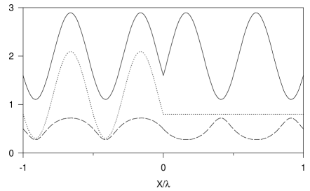
The dependence of the measured potential comes from the oscillations in the ratio of the two densities, Eq. (39). Since the injectivity is a part of the LDOS, this ratio is always between zero and one and thus, the measured potential , Eq. 39, lies always between and . If the ratio is close to one, which is often the case to the left of the scatterer, the measured potential is close to the applied electrochemical potential to the left of the scatterer . However, we can also find positions to the left of the scatterer where the ratio is small so that the measured potential is close to the electrochemical potential to the right of the scatterer . Likewise, we can also find positions to the right of the scatterer where we measure a potential which is close to the applied potential at the left side. This leads to interesting effects when the voltage probe is used to measure the resistance of a barrier.
VI The Resistance Measurement

The four-terminal resistance[19] (Fig. 4) of a scatterer is defined as the ratio of the voltage drop across the scatterer, , divided by the current flowing through the scatterer due to the applied voltage ,
| (40) | |||||
| (41) |
Here is the overall transmission probability of the conductor in the absence of the measuring contacts. Using Eq. (1) the four terminal resistance is
| (42) | |||||
| (43) |
Notice that the last expression is just the difference of two (three terminal) voltage measurements given by Eq. (39). The notion , denotes the coupling points of the voltage probes 3 and 4 in the plane of the wire. Since in the densities and interference between incoming and reflected waves is taken into account, Eq. (44) is a phase-sensitive resistance. Due to these interference effects the densities show a complicated spatial behavior, e. g. the Friedel-like oscillations in the one-channel case.
Instead of using the weak coupling contacts as voltage contacts we might also use contact 3 to inject current and contact four as the current sink. The measured resistance is then and is related to by a reciprocity relation[14, 19] . Thus this resistance is determined by the difference of the emissivities into contact of the points and ,
| (44) |
Note that both the overall transmission probability and the local densities are even functions of the magnetic field. We also remark that one might believe that current transport from one weak coupling probe to another invokes more information then is contained in the injectivities or emissivities. This not the case, since the current balance is such that to lowest order in the coupling strength of the weak coupling contacts the injected current first reaches the massive contacts and and the current at probe is determined by carriers injected by the massive contacts and . Direct transmission of carriers from one weakly coupled contact to the other one is a second order effect, proportional to , and thus, generally only a small perturbation. Chan and Heller showed recently[33] that, on surfaces with point defects (adatoms), even this second order effect can be deduced from single tip measurements.
In order to get from Eq. (43) to a position independent value for the four-terminal resistance we average the phase-sensitive result by moving the voltage probes on both sides of the scatterer over some distance while measuring the voltage. One possibility is to keep the transverse coordinates fixed and average only along the axis.
Let us now consider the one-channel case. There we know that it is sufficient to average over half a Fermi wavelength, since the measured voltages show a periodic behaviour on this length scale. We get the phase-averaged result,
| (45) | |||||
| (46) |
The same result was already found by Büttiker[12] who described the voltage probes as wave splitters.
For comparison we calculate also a phase-insensitive resistance which means that we neglect the phase coherence of incoming and reflected wave altogether. This is equivalent to averaging injectivity and local density separately and leads to the Landauer[8] formula for the resistance of a scatterer,
| (47) | |||||
| (48) |
We emphasize that what can be measured directly by using a sufficiently sharp tip is the phase-sensitive result. By moving the tip and averaging over the measured potentials we get the phase-averaged result. Note that the phase-averaged result would also be obtained if the measurement is made further then a phase-breaking length away from the scatterer.
A The few-channel case
For a scatterer connected to leads with open channels Eq. (44) is still valid. The injectivity as well as the local density are now not anymore periodic functions. They consist of a superposition of oscillations with different wavelengths. In fact, the functions contain oscillations with wave vectors given by all possible combinations of the Fermi wave vectors of the channels. If the number of channels is very large, one expects that the densities become nearly constant as a function of the position . Instead of the exact densities we can then use the densities averaged over a portion of the conductor. The injectivity of contact 1 to the left and to the right of the scatterer averaged over and are given by Eqs. (29) and (30). Using these densities in Eq. (47) gives the result of Azbel[9] and Büttiker et al. [10] found with the help of a charge neutrality argument.
Since the densities averaged over the and coordinates do not anymore exhibit a dependence on the transverse coordinate, the resulting resistance formula can not explain the magnetic field dependence (Hall effect) of the measured resistance. In contrast, Eq. (44), includes the exact, spatial densities and shows a dependence on the magnetic field not only through transmission probabilities but also due to the magnetic field dependence of the injectivity and emissivity. We will now illustrate this point by investigating the Hall resistance of a one channel wire with an obstacle.
B Magnetic field dependence of the Resistance
Let us consider a scatterer which is connected via ideal leads to two electron reservoirs. Let us assume that in the ideal lead, far away from the scatterer, we have a uniform potential in the longitudinal direction and a parabolic confining potential in the transverse direction, . Furthermore, the lead is threaded by a magnetic field perpendicular to the plane. In the lead the eigenfunctions of such a system can be written as a product of a plane wave in direction and a transverse wave function . The transverse wavefunction depends now on the vector of the plane wave in the direction. That means, that not only different channels, but also incoming and reflected waves in the same channel have different transverse wave functions. This mechanism leads to a spatial separation of incoming and reflected waves and in a strong magnetic field to the formation of edge channels[34, 35]. The Hall effect in perfect ballistic wires has been discussed[36] in connection with the suppression of the Hall effect in ballistic crosses[37]. This suppression is, however, an effect which depends on the geometry of the cross[38, 39]. Here, the main effect which we investigate arises due to the scatterer in the wire which is taken to have a magnetic field independent transmission probability .
For the case of only one open channel in the lead, the scattering state coming in from contact 1 can be written in the lead connecting the scatterer to contact 1 as
| (49) |
Here, is the reflection amplitude for reflection from contact 1 into itself, and are the wave vectors for incoming and reflected waves and and are the corresponding transverse wave functions[27]. The voltage measured on a point to the left of the scatterer is given by Eq. (39). Using Eq. (49) we find for the densities,
| (51) | |||||
| (52) | |||||
| (53) |
Here, and . The magnetic field dependence of this formula is hidden in the transverse wavefunctions.
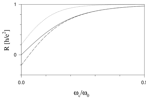
In Fig. 5 we show the measured four-terminal resistance as a function of the ratio , where is the cyclotron frequency and the magnetic field. The three curves correspond to three different configurations of the voltage probes, contact 3 and 4. The two voltage probes are placed on the two edges of the lead connecting contact one to the scatterer. First in a way that the position of the two probes is the same (solid line). Second, the coordinate of probe 3 is such that the LDOS has a minimum, , at that point in the lead, whereas probe 4 is place on a point where the LDOS has a maximum, (dashed line). And finally, probe 4 is placed over a minimum of the LDOS and probe 3 is placed over a maximum of the LDOS (dotted line). Note, that, if there is no magnetic field present, the resistance is zero, when the positions of the two probes differ only in their coordinate. If the magnetic field is turned on, a Hall-resistance develops which at strong magnetic fields reaches the quantized value . In the case, where the positions of the probes differ in the coordinate in the way described above, a non-vanishing resistance is already measured at zero magnetic field. However, when the field is turned on, both curves approach the value . For small magnetic fields, we can expand the resistance formula, Eq. (43), and get to first order in
| (55) | |||||
where is the cyclotron frequency and . In this formula, the dependent Hall resistance and the dependent, longitudinal resistance enter additively.
VII Discussion
In this work we described systems consisting of two weakly-coupled multi-probe conductors starting from the global scattering matrix of the whole system which covers all parts including the weakly coupled contact. We derived a general transmission formula, Eq. (35), for transmission through the weak-coupling contact. We have investigated this formula in the case where there is only one tunneling path. Using these expressions we can rewrite formulae, which express the resistance as functions of transmission probabilities, as functions of the local partial density of states. Applying this result the resistance of a one-channel conductor with a barrier shows interesting and surprising features. Our resistance formula can also account for the Hall-resistance. This point is illustrated using two weakly-coupled voltage-probes to measure the magnetic-field dependence of the resistance of a ballistic one-channel conductor with a barrier.
Based on the general expression, we can also treat contacts which permit multiple tunneling paths. After all, even an STM exhibits a current distribution with a certain spatial width[29]. It is then interesting to ask what the densities are which are measured by spatially extended tunneling contacts. To our knowledge, a detailed study of extended tunneling contacts has not yet been done.
We have treated the zero-temperature limit. At a non-vanishing temperature the corresponding results are obtained by multiplying the transmission probability with the Fermi function of the injecting reservoir. Even in the limit of a single tunneling path the corresponding resistances will then in general not be independent of the density of states in the tip if this density exhibits a substantial variation at the Fermi energy[31].
We have already emphasized that the density of states discussed here are quantities which are conjugate to the electrochemical potential of a contact[20]. At zero temperature they are evaluated at the Fermi energy in the equilibrium potential. The densities used here are thus essentially chemical quantities and interactions enter only through the equilibrium potential. The interaction induced portion of the density does not enter into the transmission behaviour of a conductor. This should be contrasted with the notion of tunneling-density of states which are evaluated using the unrestricted Green’s functions containing the full interaction. An investigation of this important point is beyond the scope of this work. We refer an interested reader to a discussion of the same issue concerning not density of states but directly the conductance of interacting systems[40].
We have discussed examples of voltage and resistance measurements on conductors with a single open channel. The approach discussed here, however, is also suitable for conductors having several or even a large number of open channels. For a metallic diffusive conductor of length , extending from to , with a local density of states the injectivity can be separated into an ensemble averaged part given by and a fluctuating part. The average behavior gives us the linear voltage drop and the ohmic length dependence which we expect for such conductors. More interesting is the investigation of the Hall conductance: although the local, ensemble averaged density of states of a metallic conductor is independent of the magnetic field, the injectivities exhibit a linear dependence on the magnetic field and and this gives rise to the Hall resistance, similar to the one-dimensional example discussed in Section VI.
To conclude we emphasize that the investigation of tunneling contacts on mesoscopic conductors is an interesting subject which has so far found only limited attention.
This work was supported by the Swiss National Science Foundation.
REFERENCES
- [1] Proximal Probe Microscopies, IBM J. Res. Develop. 95, Vol. 39, Nr. 6 (1985).
- [2] J. Bardeen, Phys. Rev. Lett. 6, 57 (1961).
- [3] J. Tersoff and D. R. Hamann, Phys. Rev. B 31, 805 (1985)
- [4] P. K. Hansma and J. Tersoff, J. Appl. Phys. 61, R1 (1987)
- [5] P. Muralt, H. Meier, D. W. Pohl, and H. W. M. Salemink, Appl. Phys. Lett. 50, 1352 (1987).
- [6] J. R. Kirtley, S. Washburn, and M. J. Brady, Phys. Rev. Lett. 60, 1546 (1988)
- [7] H.-L. Engquist and P. W. Anderson, Phys. Rev. B 24, 1151 (1981)
- [8] R. Landauer, Phil. Mag. 21, 863 (1970); IBM J. Res. Develop. 1, 223 (1957).
- [9] M. Ya. Azbel, J. Phys. C 14, L225 (1981)
- [10] M. Büttiker, Y. Imry, R. Landauer, and S. Pinhas, Phys. Rev. B 31, 6207 (1985).
- [11] Y. Imry, in Directions in Condensed Matter Physics, edited by G. Grinstein and G. Mazenko, (World Scientific Singapore, 1986). p. 101.; see also O. Entin-Wohlmann, C. Hartzstein, and Y. Imry, Phys. Rev. B 34, 921 (1986).
- [12] M. Büttiker, Phys. Rev. B 40, 3409 (1989).
- [13] A. D. Stone, Phys. Rev. Lett. 54, 2692 (1985).
- [14] M. Büttiker, Phys. Rev. Lett. 57, 1761 (1986).
- [15] Y. Hasegawa and Ph. Avouris, Phys. Rev. Lett. 71, 1071 (1993)
- [16] Ph. Avouris, Solid State Communications 92, 11 (1994)
- [17] M. F. Crommie, C. P. Lutz, and D. M. Eigler, Science 262, 218 (1993)
- [18] C. S. Chu and R. S. Sorbello, Phys. Rev. B 42, 4928 (1990)
- [19] M. Büttiker, IBM J. Res. Develop. 32, 317 (1988).
- [20] M. Büttiker, J. Phys.: Condens. Matter 5, 9361 (1993)
- [21] V. Gasparian, T. Christen, and M. Büttiker, Phys. Rev. A 54, 4022 (1996)
- [22] M. Büttiker and T. Christen, in Quantum Transport in Semiconductor Submicron Structures, edited by B. Kramer, (Kluwer Academic Publishers, Dordrecht, 1996); NATO ASI Series, Vol. 326, 263 -291 (1996).
- [23] J. J. M. Verbaarschot, H. A. Weidenmüller, and M. R. Zirnbauer, Phys. Rep. 129, 367 (1985)
- [24] S. Iida, H. A. Weidenmüller, and J. Zuk, Phys. Rev. Lett. 64, 583 (1990); Ann. Phys. (N.Y.) 200, 219 (1990)
- [25] C. H. Lewenkopf and H. A. Weidenmüller, Ann. Phys. (N.Y.) 212, 53 (1991)
- [26] P. W. Brouwer and M. Büttiker, Europhys. Lett. 37, 441 (1997).
- [27] S. Datta, Electronic Transport in Mesoscopic Conductors, Cambridge University Press, 1995.
- [28] C. R. Leavens, and G. C. Aers, Solid State Commun. 67, 1135 (1988).
- [29] N. D. Lang, Phys. Rev. B 36, 8173 (1987).
- [30] J. B. Pendry, A. B. Prêtre, and B. C. H. Krutzen, J. Phys.: Condens. Matter 3, 4313 (1991).
- [31] A. Levy-Yeyati and A. Flores, (unpublished). For instance tunneling tips might contain resonant states.
- [32] I. B. , Levinson, Sov. Phys. JETP 68, 1257 (1989).
- [33] Yick Stella Chan and J. E. Heller, Phys. Rev. Lett. 78, 2570 (1997).
- [34] P. Streda, J. Kucera, and A. H. MacDonald, Phys. Rev. Lett. 59, 1973 (1987).
- [35] M. Büttiker, Phys. Rev. B 38, 9375 (1988).
- [36] F. M. Peeters, Phys. Rev. Lett. 61, 589 (1988); Y. Imry, in Nanostructure Physics and Fabrication, edited by M. A. Reed and W. P. Kirk, (Academic Press, Inc. 1989), p. 379; D. P. Chu, and P. Butcher, J. Phys.: Condens. Matter 5, L397, (1993); Phys. Rev. B 47, 10008 (1993).
- [37] M. L. Roukes, A. Scherer, S. J. Allen, Jr., H. G. Craighead, R. M. Ruthen, E. D. Beebe, and J. P. Harbison, Phys. Rev. Lett. 59, 3011 (1988); A. M. Chang, T. Y. Chang, and H. U. Baranger, Phys. Rev. Lett. 63, 996 (1989).
- [38] C. J. B. Ford, S. Washburn, M. Büttiker, C. M. Knoedler, and J. M. Hong, Phys. Rev. Lett. 62, 2724 (1989).
- [39] C. W. J. Beenakker, and H. van Houten, Phys. Rev. Lett. 60, 2406 (1988); H. U. Baranger and A. D. Stone, Phys. Rev. Lett. 63, 414 (1989).
- [40] A. Yu. Alekseev, V. V. Cheianov, and J. Frölich, (unpublished). cond-mat/9706061