[
Minimum Metallic Mobility in a Two-Dimensional Electron Gas
Abstract
We report the observation of a metal-insulator transition in a two-dimensional electron gas in silicon. By applying substrate bias, we have varied the mobility of our samples, and observed the creation of the metallic phase when the mobility was high enough (1 m2/Vs), consistent with the assertion that this transition is driven by electron-electron interactions. In a perpendicular magnetic field, the magnetoconductance is positive in the vicinity of the transition, but negative elsewhere. Our experiment suggests that such behavior results from a decrease of the spin-dependent part of the interaction in the vicinity of the transition.
pacs:
PACS Nos. 71.30.+h, 73.40.Qv]
Following the development of the scaling theory of localization for non-interacting electrons [1], it has been widely believed that there is no metal-insulator transition (MIT) in two dimensions, in agreement with early experiments [2] on a two-dimensional electron gas (2DEG) in low-mobility (0.2–0.65 mVs) Si metal-oxide-semiconductor field-effect transistors (MOSFETs). However, recent experiments [3] on high-mobility (2–7 mVs) MOSFETs have provided clear evidence for the existence of a MIT in this 2D system, raising speculation that this transition is driven by electron-electron interactions. In an entirely different experiment [4] on mesoscopic Si MOSFETs of comparable quality (peak mobility 2 mVs), non-monotonic behavior of several characteristic energy scales was found in the transition region, in clear contradiction with general considerations based on non-interacting models [1]. The apparent conflict between these experiments and the scaling theory of localization has been resolved recently by formulating a scaling theory for interacting electrons [5], which shows that the existence of a 2D MIT does not contradict any general scaling idea or principle. So far, however, it has not been shown experimentally how the results of Ref. [3] can be reconciled with those obtained on low-mobility samples [2]. It is exactly this issue that our current work resolves.
We present the results obtained on a 2DEG in Si MOSFETs with a peak mobility of 0.5–0.8 mVs at 4.2 K. In these samples, all electronic states are localized, in agreement with early studies [2]. By applying the substrate bias, however, we have been able to increase the peak mobility to 1 mVs, and observe the metal-insulator transition. As shown below, the resulting scaling behavior of the conductivity with temperature is in excellent agreement with the results of Ref. [3]. Therefore, in this way one can study, on a single sample, the emergence of the metallic phase once the mobility becomes sufficiently high at low carrier densities, where the Coulomb interaction is an order of magnitude greater than the Fermi energy. In addition, our magnetoconductance measurements in a weak perpendicular field show that the spin-dependent part of the electron-electron interaction decreases sharply at the transition.
Our measurements were carried out on n-channel MOSFETs fabricated on the (100) surface of Si doped at acceptors/cm3 with 435 Å gate oxide thickness and oxide charge cm-2. The samples had a Corbino (circular) geometry with the channel length mm and width mm. Conductance was measured as a function of gate voltage (proportional to carrier density ) at temperatures K, using a lock-in at a frequency of Hz and an excitation voltage of 0.3 mV.
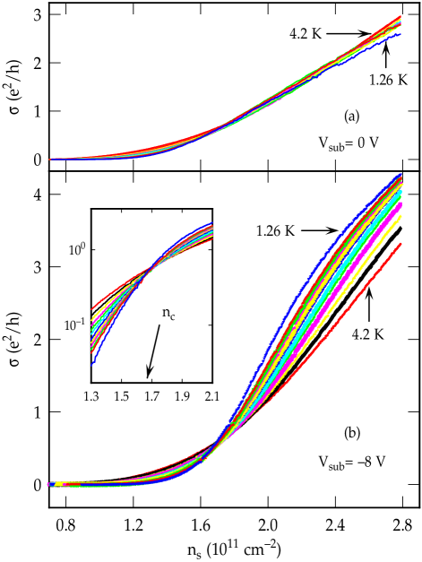
Fig. 1(a) shows the conductivity for one of the samples (sample #5), as a function of for several temperatures and with no substrate bias applied. As is lowered, decreases for both low and high , indicating insulating behavior. The temperature dependence is weaker at intermediate values of .
Application of a substrate bias in Si MOSFETs at a given changes the electric field at the Si-SiO2 interface. As a result, the average
position of the 2D electrons with respect to the interface is changed as well as the splitting between the subbands [6]. (At low temperatures, all electrons populate only the lowest subband and, therefore, are confined to motion only in the plane parallel to the Si-SiO2 interface.) The reverse moves the electrons closer to the interface. In some samples, especially those with lightly doped substrates such as ours, where the subband splitting is comparatively small, the mobility is enhanced [7]. This has been attributed to the reduction of scattering of the 2DEG by electrons that occupy very long band tails associated with upper subbands and act as additional scattering centers. The reverse increases the subband splitting and makes this scattering mechanism less important. It may also reduce the average effective mass since the upper subband electrons are heavier. In addition, the reverse reduces the average spatial extent of the inversion layer charge density in the direction perpendicular to the interface (typically, Å [6]).
We find, for example, that V leads to a slight increase of and the merging of different temperature curves over a wide range of , roughly between 1.8 and cm-2. At the highest , the temperature dependence of still indicates insulating behavior. The reason for the merging at intermediate values of becomes clear upon the application of an even higher (reverse) , as shown in Fig. 1(b) for V: the temperature dependent behavior of is now reversed for all above some critical electron density (cm-2 for sample #5), as expected for metallic behavior. For , the 2DEG exhibits insulating behavior as before. We have obtained similar results on another sample (sample #1), where V was used to raise the peak mobility to 1 mVs, and study the metal-insulator transition at cm-2.
The results displayed in Fig. 1(b) are very similar to those reported in Ref. [3], where it was also found that the resistivity scales with temperature near the transition according to
| (1) |
with a single parameter that is the same function of on both the metallic and the insulating side of the transition, . Here is the dynamical exponent, and is the correlation length exponent. The results of this scaling for the data in Fig. 1(b) are shown in Fig. 2. All the data collapse onto two
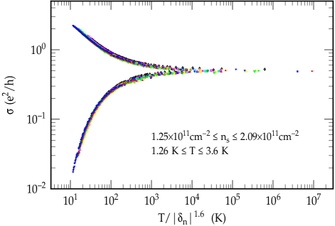
branches, the upper one for the metallic side of the transition, and the lower one for the insulating side. The best collapse is found for , where quite a wide range of electron densities (with up to 0.25) was used. For sample #1, we find that . These results are in a remarkable agreement with experiments on high-mobility MOSFETs [3]. We find that the critical conductivity for sample #5, and for sample #1, consistent with the reported [3] values and suggesting that the critical conductivity has a value around .
The scaling theory predicts [5] that, to leading order, the temperature dependence of the conductivity in the critical region associated with the metal-insulator transition will be given by
| (2) |
where is an unknown constant. In other words, the temperature dependence of is predicted to be exponential on both insulating and metallic sides of the transition, and with the same exponent. This symmetry is expected to hold only for , i. e. the quantum critical region is defined by the temperature scale . The data presented in Fig. 2 are shown again in Fig. 3 as a function of , with . They are consistent with the
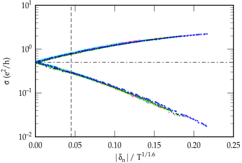
theory, and we observe the symmetry for of up to 0.045. This value defines , and we find that . For the range of temperatures of up to 3.6 K, for which scaling works, this means that the quantum critical region extends at most up to .
We have performed careful magnetoconductance measurements in perpendicular magnetic fields of up to 1 T. Fig. 4(a) shows magnetoconductance (MC), defined as , for sample #1 with V, for several

carrier densities in the critical region. As the (zero-field) critical density is approached from the metallic side, the positive MC develops gradually, reaches a maximum at T when , and then it disappears gradually on the insulating side. Exactly the same behavior is found in high-mobility mesoscopic Si MOSFETs [8] at much lower temperatures, down to 40 mK. At higher , and for outside this narrow critical region, MC is always negative. The dependence of MC on is displayed clearly in Fig. 4(b) for several magnetic fields. MC exhibits a pronounced maximum at .
Obviously, there are positive and negative contributions to the measured MC. It is well established that the positive MC can result from quantum interference effects in both weakly [9] and strongly [10, 11] disordered systems. The spin-dependent part of the electron-electron interaction [9] gives rise to negative MC, at least in the weakly disordered regime. This has been well established in doped semiconductors [12], and large negative MC has been seen in high-mobility MOSFETs for parallel to the current plane [13]. In all cases, one expects in the low-field limits, becoming weaker for higher than some characteristic field. In case of weak localization, the characteristic field is reached when the Landau orbit size becomes comparable to the thermal length, i. e. when , where is the diffusion constant [9], so that T for our samples. In our experiment, MC changes sign and becomes negative at sufficiently high for all in the critical region (). We, therefore, conclude that the positive contribution is no longer in the low-field limit, consistent with the estimate of T. On the other hand, there is a negative, predominantly quadratic -dependence at the highest fields, indicating that the negative contribution to the MC is still in the low-field regime. This is consistent with the estimated characteristic field for the MC due to spin splitting in an interacting electron gas, given by the condition that the Zeeman energy is comparable to the thermal energy, i. e. [9], and for [14], K at T.
In order to understand the puzzling -dependence of MC [Fig. 4(b)], it is desirable to disentangle the two contributions. Obviously, the MC in our samples can be described by
| (3) |
with . We find that, for T, has the same form, up to a constant (), for all . Fig. 5(a) shows that different curves are indeed indistinguishable to within the scatter of data and, therefore, independent of . In this way, we have been able to determine the change in as is varied, independent of the choice of . In order to obtain the absolute values of to show in Fig. 5, we have used [15]. Fig. 5(b) presents both the positive (: open symbols) and the negative contribution (: solid symbols) as a function of

for T. The positive MC due to quantum interference does not depend on within the scatter of data. On the other hand, the negative contribution, i. e. , has a strong minimum at the metal-insulator transition.
In summary, we have shown that the metallic phase can be created in a 2DEG by increasing its mobility, consistent with the assertion that the 2D MIT is driven by electron-electron interactions. We have also shown that the negative part of the MC, determined by the spin-dependent part of the interaction, decreases sharply at the transition. We point out striking similarities between transport properties of a 2DEG in Si MOSFETs and those observed in Si:B, which is a 3D system: (a) the -dependence is qualitatively the same, i. e. increases with decreasing in the metallic phase [16]; (b) magnetoconductance, which is negative in Si:B, depends strongly on the carrier concentration and shows a dramatic decrease at the transition [17]. We recall that such anomalous behavior has been attributed to electron-electron interactions in the case of Si:B. Our experiment suggests the possibility that electron-electron interactions may play a similar role in both 2D and 3D systems near the metal-insulator transition.
The authors are grateful to V. Dobrosavljević for useful discussions. This work was supported by NSF Grant No. DMR-9510355.
REFERENCES
- [1] E. Abrahams, P.W. Anderson, D.C. Licciardello, and T.V. Ramakrishnan, Phys. Rev. Lett. 42, 673 (1979).
- [2] D.J. Bishop, D.C. Tsui, and R.C. Dynes, Phys. Rev. Lett. 44, 1153 (1980); M.J. Uren, R.A. Davies, and M. Pepper, J. Phys. C: Solid St. Phys. 13, L985 (1980).
- [3] S.V. Kravchenko, G.V. Kravchenko, J.E. Furneaux, V.M. Pudalov, and M. D’Iorio, Phys. Rev. B 50 8039 (1994); S.V. Kravchenko, Whitney E. Mason, G.E. Bowker, J.E. Furneaux, V.M. Pudalov, and M. D’Iorio, Phys. Rev. B 51, 7038 (1995); S.V. Kravchenko, D. Simonian, M.P. Sarachik, Whitney Mason, and J.E. Furneaux, Phys. Rev. Lett. 77, 4938 (1996).
- [4] Dragana Popović and S. Washburn, preprint cond-mat/9612021.
- [5] V. Dobrosavljević, E. Abrahams, E. Miranda, and Sudip Chakravarty, preprint cond-mat/9704091.
- [6] See T. Ando, A.B. Fowler, and F. Stern, Rev. Mod. Phys. 54, 437 (1982).
- [7] A.B. Fowler, Phys. Rev. Lett. 34, 15 (1975).
- [8] Kuo-Ping Li, Dragana Popović, and S. Washburn (unpublished).
- [9] P.A. Lee and T.V. Ramakrishnan, Rev. Mod. Phys. 57, 287 (1985).
- [10] V.L. Nguyen, B.Z. Spivak, and B.I. Shklovskii, Sov. Phys. JETP 62, 1021 (1985).
- [11] U. Sivan, O. Entin-Wohlman, and Y. Imry, Phys. Rev. Lett. 60, 1566 (1988); O. Entin-Wohlman, Y. Imry, and U. Sivan, Phys. Rev. B 40, 8342 (1989).
- [12] S. Bogdanovich, P. Dai, M.P. Sarachik, and V. Dobrosavljević, Phys. Rev. Lett. 74, 2543 (1995).
- [13] D. Simonian, S.V. Kravchenko, and M.P. Sarachik, preprint cond-mat/9704071.
- [14] g-factor may be enhanced up to at low : see Sudhakar Yarlagadda and Gabriele F. Giuliani, Phys. Rev. B 49, 14188 (1994).
- [15] The form of the function cannot be determined precisely from the existing data, but our qualitative conclusions do not depend on the choice of .
- [16] P. Dai, Y. Zhang, and M.P. Sarachik, Phys. Rev. Lett. 66, 1914 (1991).
- [17] S. Bogdanovich, P. Dai, M.P. Sarachik, V. Dobrosavljević, and G. Kotliar, Phys. Rev. B 55, 4215 (1997).